
2001-2012 Microchip Technology Inc.
Preliminary
DS21655C-page 1
MCP2150
Features
• Implements the IrDA
®
standard including:
- IrLAP
- IrLMP
- IAS
- TinyTP
- IrCOMM (9-wire “cooked” service class)
• Provides IrDA standard physical signal layer
support including:
- Bidirectional communication
- CRC implementation
- Data communication rates up to 115.2 kbaud
• Includes UART to IrDA standard encoder/decoder
functionality:
- Easily interfaces with industry standard
UARTs and infrared transceivers
• UART interface for connecting to Data Terminal
Equipment (DTE) systems
• Transmit/Receive formats (bit width) supported:
- 1.63 µs
• Hardware baud rate selection for UART:
- 9.6 kbaud
- 19.2 kbaud
- 57.6 kbaud
- 115.2 kbaud
• Infrared baud rates supported:
- 9.6 kbaud
- 19.2 kbaud
- 38.4 kbaud
- 57.6 kbaud
- 115.2 kbaud
• 64 Byte Data Packet Size
• Programmable Device ID String
• Operates as Secondary Device
CMOS Technology
• Low power, high-speed CMOS technology
• Fully static design
• Low voltage operation
• Industrial temperature range
• Low power consumption
- < 1 mA @ 3.3 V, 11.0592 MHz (typical)
- 3 µA typical @ 5.0 V when disabled
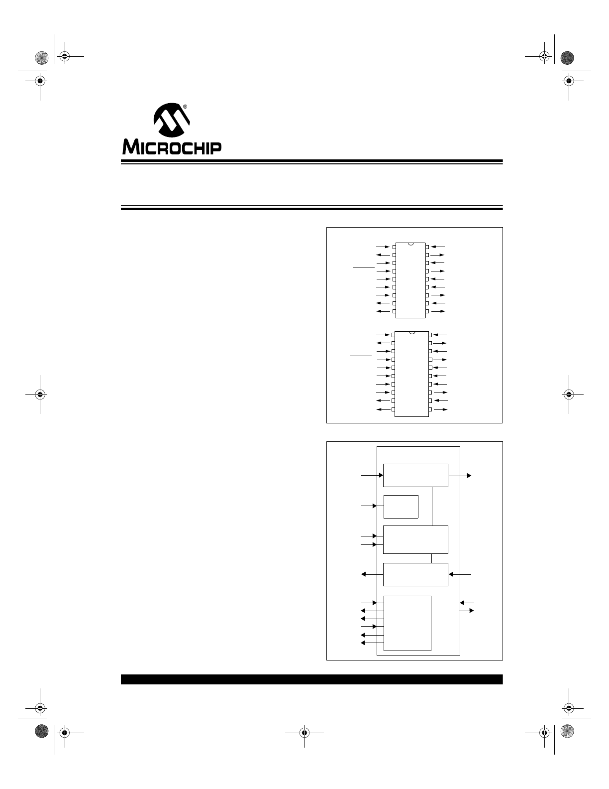
Package Types
Block Diagram
2
3
4
5
6
7
8
9
10
1
2
3
4
5
6
7
8
9
1
19
18
16
15
14
13
12
11
17
18
17
15
14
13
12
11
10
16
20
OSC2
OSC1/CLKI
V
SS
V
SS
V
DD
V
DD
BAUD1
CD
CTS
RTS
TX
RX
RI
DSR
DTR
TXIR
RXIR
RESET
EN
BAUD0
V
SS
TX
RX
RI
TXIR
RXIR
RESET
EN
BAUD0
OSC2
OSC1/CLKI
V
DD
BAUD1
CD
CTS
RTS
DSR
DTR
MC
P2
150
M
C
P
215
0
PDIP, SOIC
SSOP
Encode and
Protocol Handler
TX
TXIR
RX
RXIR
EN
MCP2150
Logic
Baud Rate
RTS
Generator
BAUD1
BAUD0
CD
UART
Control
CTS
DSR
DTR
RI
OSC1
OSC2
Protocol Handler
and Decode
IrDA
®
Standard Protocol Stack Controller
Supporting DTE Applications
21655C.book Page 1 Thursday, January 10, 2013 12:57 PM

MCP2150
DS21655C-page 2
Preliminary
2001-2012 Microchip Technology Inc.
NOTES:
21655C.book Page 2 Thursday, January 10, 2013 12:57 PM

2001-2012 Microchip Technology Inc.
Preliminary
DS21655C-page 3
MCP2150
1.0
DEVICE OVERVIEW
This document contains device specific information for
the following device:
• MCP2150
The MCP2150 is a cost effective, low pin count (18-pin),
easy to use device for implementing IrDA standard wire-
less connectivity. The MCP2150 provides support for
the IrDA standard protocol “stack” plus bit encoding/
decoding.
The serial interface baud rates are user selectable to
one of four IrDA standard baud rates between 9600
baud and 115.2 kbaud (9600, 19200, 57600, 115200).
The IR baud rates are user selectable to one of five
IrDA standard baud rates between 9600 baud and
115.2 kbaud (9600, 19200, 37400, 57600, 115200).
The serial interface baud rate will be specified by the
BAUD1:BAUD0 pins, while the IR baud rate is specified
by the Primary Device (during Discover phase). This
means that the baud rates do not need to be the same.
The MCP2150 operates in Data Terminal Equipment
(DTE) applications and sits between a UART and an
infrared optical transceiver.
The MCP2150 encodes an asynchronous serial data
stream, converting each data bit to the corresponding
infrared (IR) formatted pulse. IR pulses received are
decoded and then handled by the protocol handler
state machine. The protocol handler sends the appro-
priate data bytes to the Host Controller in UART
formatted serial data.
The MCP2150 supports “point-to-point” applications.
That is, one Primary device and one Secondary device.
The MCP2150 operates as a Secondary device. It does
not support “multi-point” applications.
Sending data using IR light requires some hardware
and the use of specialized communication protocols.
These protocol and hardware requirements are
described, in detail, by the IrDA standard specifica-
tions. The encoding/decoding functionality of the
MCP2150 is designed to be compatible with the physi-
cal layer component of the IrDA standard. This part of
the standard is often referred to as “IrPHY”.
The complete IrDA standard specifications are avail-
able for download from the IrDA website
(www.IrDA.org).
21655C.book Page 3 Thursday, January 10, 2013 12:57 PM
MCP2150
DS21655C-page 4
Preliminary
2001-2012 Microchip Technology Inc.
1.1
Applications
The MCP2150 Infrared Communications Controller
supporting the IrDA standard provides embedded sys-
tem designers the easiest way to implement IrDA stan-
dard wireless connectivity.
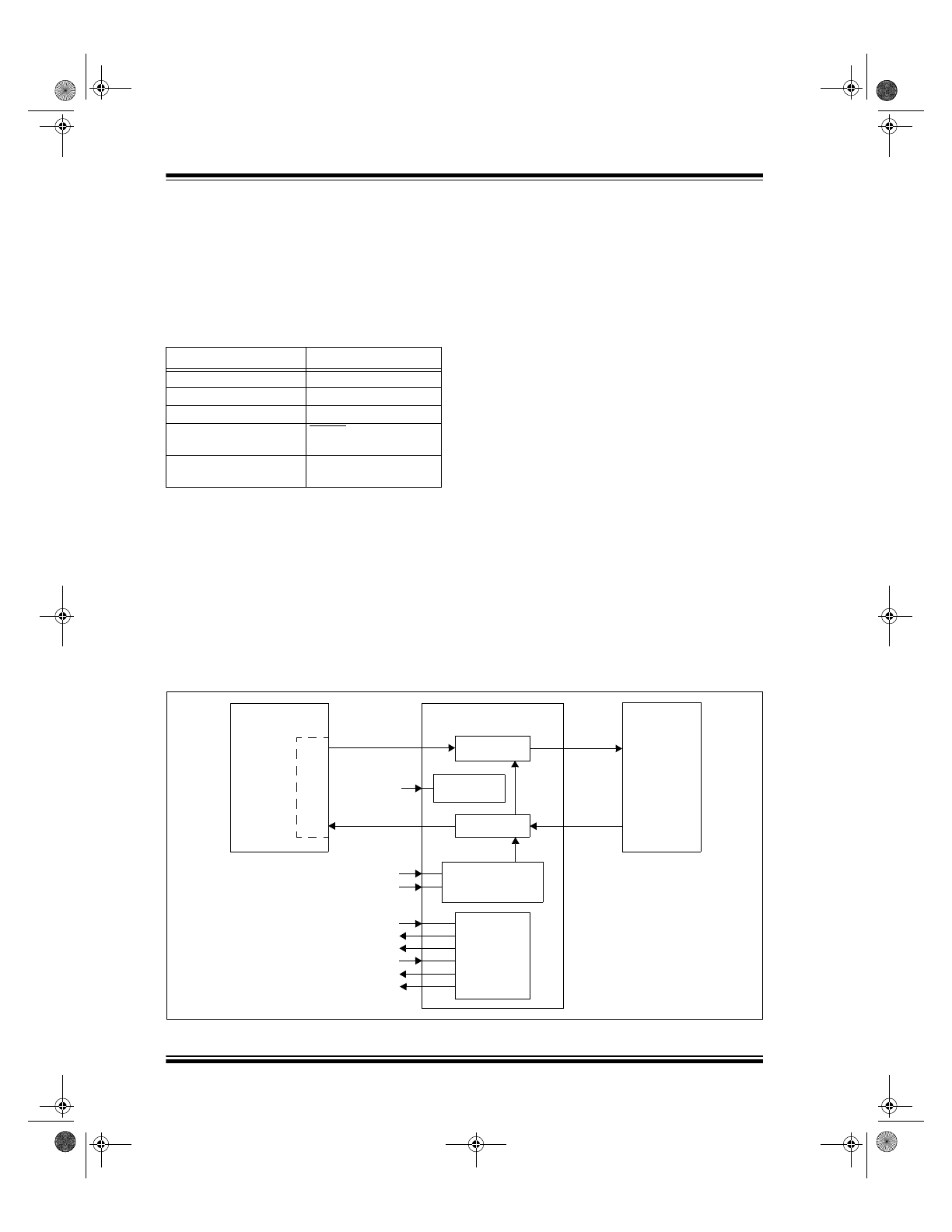
Figure 1-1
shows a typical
application block diagram.
Table 1-2
shows the pin
definitions.
TABLE 1-1:
OVERVIEW OF FEATURES
Infrared communication is a wireless two-way data
connection, using infrared light generated by low-cost
transceiver signaling technology. This provides reliable
communication between two devices.
Infrared technology offers:
• Universal standard for connecting portable
computing devices
• Easy, effortless implementation
• Economical alternative to other connectivity
solutions
• Reliable, high-speed connection
• Safe to use in any environment (can even be
used during air travel)
• Eliminates the hassle of cables
• Allows PCs and other electronic devices (such as
PDAs, cell phones, etc.) to communicate with
each other
• Enhances mobility by allowing users to easily
connect
The MCP2150 allows the easy addition of IrDA stan-
dard wireless connectivity to any embedded applica-
tion that uses serial data.
Figure 1-1
shows typical
implementation of the MCP2150 in an embedded
system.
The IrDA protocols for printer support are not included
in the IrCOMM 9-wire “cooked” service class.
FIGURE 1-1:
SYSTEM BLOCK DIAGRAM
Features
MCP2150
Serial Communications
UART, IR
Baud Rate Selection
Hardware
Low Power Mode
Yes
Resets (and Delays)
RESET, POR
(PWRT and OST)
Packages
18-pin DIP, SOIC,
20-pin SSOP
Encode
Decode
TX
TXIR
RX
RXIR
EN
MCP2150
Host Controller
TX
RX
Optical
UA
R
T
TXD
RXD
Power Down
Logic
Baud Rate
Generator
BAUD1
BAUD0
RTS
CD
UART
Control
CTS
DSR
DTR
RI
Transceiver
(Microcontroller)
21655C.book Page 4 Thursday, January 10, 2013 12:57 PM
2001-2012 Microchip Technology Inc.
Preliminary
DS21655C-page 5
MCP2150
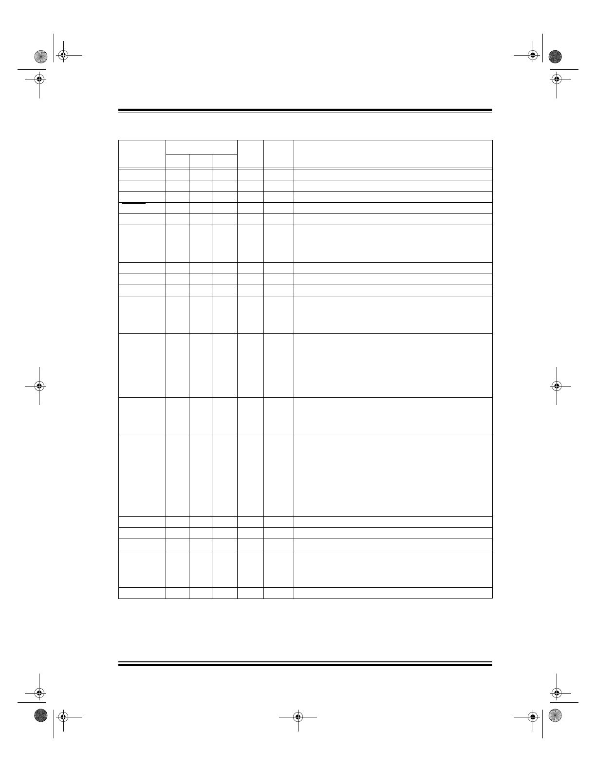
TABLE 1-2:
PIN DESCRIPTIONS
Pin Name
Pin Number
Pin
Type
Buffer
Type
Description
PDIP SOIC SSOP
BAUD0
1
1
1
I
ST
BAUD1:BAUD0 specify the baud rate of the device.
TXIR
2
2
2
O
—
Asynchronous transmit to Infrared transceiver.
RXIR
3
3
3
I
ST
Asynchronous receive from Infrared transceiver.
RESET
4
4
4
I
ST
Resets the device.
V
SS
5
5
5, 6
—
P
Ground reference for logic and I/O pins.
EN
6
6
7
I
TTL
Device enable.
1
= Device is enabled.
0
= Device is disabled (low power). MCP2150 only monitors
this pin when in the NDM state.
TX
7
7
8
I
TTL
Asynchronous receive; from Host Controller UART.
RX
8
8
9
O
—
Asynchronous transmit; to Host Controller UART.
RI
9
9
10
—
—
Ring Indicator. The value on this pin is driven high.
DSR
10
10
11
O
—
Data Set Ready. Indicates that the MCP2150 has completed
reset.
1
= MCP2150 is initialized.
0
= MCP2150 is not initialized.
DTR
11
11
12
I
TTL
Data Terminal Ready. The value of this pin is ignored once
the MCP2150 is initialized. It is recommended that this pin be
connected so that the voltage level is either V
SS
or V
CC
. At
device power up, this signal is used with the RTS signal to
enter device ID programming.
1
= Enter Device ID programming mode (if RTS is cleared).
0
= Do not enter Device ID programming mode.
CTS
12
12
13
O
—
Clear to Send. Indicates that the MCP2150 is ready to
receive data from the Host Controller.
1
= Host Controller should not send data.
0
= Host Controller may send data.
RTS
13
13
14
I
TTL
Request to Send. Indicates that a Host Controller is ready to
receive data from the MCP2150. The MCP2150 prepares to
send data, if available.
1
= Host Controller not ready to receive data.
0
= Host Controller ready to receive data.
At device power up, this signal is used with the DTR signal to
enter device ID programming.
1
= Do not enter Device ID programming mode.
0
= Enter Device ID programming mode (if DTR is set).
V
DD
14
14
15, 16
—
P
Positive supply for logic and I/O pins.
OSC2
15
15
17
O
—
Oscillator crystal output.
OSC1/CLKIN
16
16
18
I
CMOS
Oscillator crystal input/external clock source input.
CD
17
17
19
O
—
Carrier Detect. Indicates that the MCP2150 has established a
valid link with a Primary Device.
1
= An IR link has not been established (No IR Link).
0
= An IR link has been established (IR Link).
BAUD1
18
18
20
I
ST
BAUD1:BAUD0 specify the baud rate of the device.
Legend:
TTL = TTL compatible input
I = Input
P = Power
ST = Schmitt Trigger input with CMOS levels
O = Output
CMOS = CMOS compatible input
21655C.book Page 5 Thursday, January 10, 2013 12:57 PM

MCP2150
DS21655C-page 6
Preliminary
2001-2012 Microchip Technology Inc.
1.1.1
SIGNAL DIRECTIONS
Table 1-3
shows the direction of the MCP2150 signals.
The MCP2150 is designed for use in Data Terminal
Equipment (DTE) applications.
TABLE 1-3:
MCP2150 SIGNAL DIRECTION
DB-9
Pin No.
Signal
Direction
Comment
1
CD
MCP2150
HC
Carrier Detect
2
RX
MCP2150
HC
Received Data
3
TX
HC
MCP2150
Transmit Data
4
DTR
(1)
—
Data Terminal
Ready
5
GND
—
Ground
6
DSR
MCP2150
HC
Data Set Ready
7
RTS
HC
MCP2150
Request to Send
8
CTS
MCP2150
HC
Clear to Send
9
RI
(1)
—
Ring
Indicator
Legend: HC = Host Controller
Note
1:
This signal is not implemented in the MCP2150.
21655C.book Page 6 Thursday, January 10, 2013 12:57 PM
2001-2012 Microchip Technology Inc.
Preliminary
DS21655C-page 7
MCP2150
2.0
DEVICE OPERATION
The MCP2150 is a cost effective, low pin count (18-
pin), easy to use device for implementing IrDA stan-
dard wireless connectivity. The MCP2150 provides
support for the IrDA standard protocol “stack” plus bit
encoding/decoding. The Serial interface and IR baud
rates are independantly selectable.
2.1
Power Up
Any time the device is powered up (
parameter D003
),
the Power Up Timer delay (
parameter 33
) occurs, fol-
lowed by an Oscillator Start-up Timer (OST) delay
(
parameter 32
). Once these delays complete, commu-
nication with the device may be initiated. This commu-
nication is from both the infrared transceiver’s side as
well as the controller’s UART interface.
2.2
Device Reset
The MCP2150 is forced into the reset state when the
RESET pin is in the low state. Once the RESET pin is
brought to a high state, the Device Reset sequence
occurs. Once the sequence completes, functional
operation begins.
2.3
Clock Source
The MCP2150 requires a clock source to operate. The
frequency of this clock is 11.0592 MHz (electrical spec-
ification
parameter 1A
). This clock can be supplied by
either a crystal/resonator or as an external clock input.
2.3.1
CRYSTAL OSCILLATOR / CERAMIC
RESONATORS
A crystal or ceramic resonator can be connected to the
OSC1 and OSC2 pins to establish oscillation
(
Figure 2-1
). The MCP2150 oscillator design requires
the use of a parallel cut crystal. Use of a series cut crys-
tal may give a frequency outside of the crystal
manufacturers specifications.
FIGURE 2-1:
CRYSTAL OPERATION
(OR CERAMIC
RESONATOR)
TABLE 2-1:
CAPACITOR SELECTION FOR
CERAMIC RESONATORS
TABLE 2-2:
CAPACITOR SELECTION FOR
CRYSTAL OSCILLATOR
2.3.2
EXTERNAL CLOCK IN
For applications where a clock is already available
elsewhere, users may directly drive the MCP2150 pro-
vided that this external clock source meets the AC/DC
timing requirements listed in
Section 4.3
.
Figure 2-2
shows how an external clock circuit should be
configured.
FIGURE 2-2:
EXTERNAL CLOCK INPUT
OPERATION
See
Table 2-1
and
Table 2-2
for recommended values of
C1 and C2.
Note:
A series resistor may be required for AT
strip cut crystals.
C1
C2
XTAL
OSC2
RS
OSC1
RF
To internal
MCP2150
Note
logic
Freq
OSC1 (C1)
OSC2 (C2)
11.0592 MHz
10 - 22 pF
10 - 22 pF
Higher capacitance increases the stability of the oscil-
lator but also increases the start-up time. These val-
ues are for design guidance only. Since each
resonator has its own characteristics, the user should
consult the resonator manufacturer for appropriate
values of external components.
Freq
OSC1 (C1)
OSC2 (C2)
11.0592 MHz
15 - 30 pF
15 - 30 pF
Higher capacitance increases the stability of the oscil-
lator but also increases the start-up time. These val-
ues are for design guidance only. R
S
may be required
to avoid overdriving crystals with low drive level spec-
ification. Since each crystal has its own
characteristics, the user should consult the crystal
manufacturer for appropriate values of external
components.
Clock From
external
MCP2150
OSC1
OSC2
Open
system
21655C.book Page 7 Thursday, January 10, 2013 12:57 PM

MCP2150
DS21655C-page 8
Preliminary
2001-2012 Microchip Technology Inc.
2.4
Bit Clock
The device crystal is used to derive the communication
bit clock (BITCLK). There are 16 BITCLKs for each bit
time. The BITCLKs are used for the generation of the
start bit and the eight data bits. The stop bit uses the
BITCLK when the data is transmitted (not for
reception).
This clock is a fixed frequency and has minimal
variation in frequency (specified by crystal
manufacturer).
2.5
UART Interface
The UART interface communicates with the "control-
ler". This interface is a half duplex interface, meaning
that the system is either transmitting or receiving, but
not both simultaneously.
2.5.1
BAUD RATE
The baud rate for the MCP2150 serial port (the TX and
RX pins) is configured by the state of the BAUD1 and
BAUD0 pins. These two device pins are used to select
the baud rate at which the MCP2150 will transmit and
receive serial data (not IR data).
Table 2-3
shows the
baud rate configurations.
TABLE 2-3:
SERIAL BAUD RATE
SELECTION VS. FREQUENCY
2.5.2
TRANSMITTING
When the controller sends serial data to the MCP2150,
the controller’s baud rate is required to match the baud
rate of the MCP2150’s serial port.
2.5.3
RECEIVING
When the controller receives serial data from the
MCP2150, the controller’s baud rate is required to
match the baud rate of the MCP2150’s serial port.
BAUD1:BAUD0
Baud Rate @
11.0592 MHz
Bit Rate
00
9600
F
OSC
/ 1152
01
19200
F
OSC
/ 576
10
57600
F
OSC
/ 192
11
115200
F
OSC
/ 96
21655C.book Page 8 Thursday, January 10, 2013 12:57 PM
2001-2012 Microchip Technology Inc.
Preliminary
DS21655C-page 9
MCP2150
2.6
Modulation
The data that the MCP2150 UART received (on the TX
pin) that needs to be transmitted (on the TXIR pin) will
need to be modulated. This modulated signal drives the
IR transceiver module.
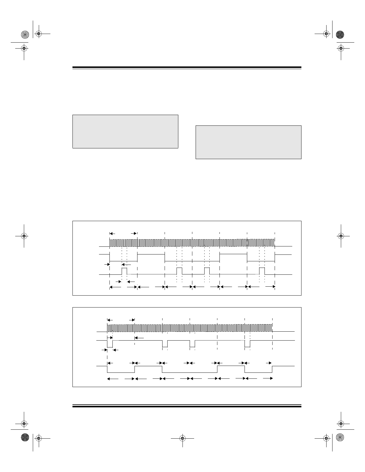
Figure 2-3
shows the encoding
of the modulated signal.
Each bit time is comprised of 16-bit clocks. If the value
to be transmitted (as determined by the TX pin) is a
logic low, then the TXIR pin will output a low level for
7-bit clock cycles, a logic high level for 3-bit clock
cycles or a minimum of 1.6 µsec. (see
parameter
IR121
). The remaining 6-bit clock cycles will be low. If
the value to transmit is a logic high, then the TXIR pin
will output a low level for the entire 16-bit clock cycles.
2.7
Demodulation
The modulated signal (data) from the IR transceiver
module (on RXIR pin) needs to be demodulated to form
the received data (on RX pin). Once demodulation of
the data byte occurs, the data that is received is trans-
mitted by the MCP2150 UART (on the RX pin).
Figure 2-4
shows the decoding of the modulated
signal.
Each bit time is comprised of 16-bit clocks. If the value
to be received is a logic low, then the RXIR pin will be
a low level for the first 3-bit clock cycles or a minimum
of 1.6 µs. The remaining 13-bit clock cycles (or differ-
ence up to the 16-bit clock time) will be high. If the value
to be received is a logic high, then the RXIR pin will be
a high level for the entire 16-bit clock cycles. The level
on the RX pin will be in the appropriate state for the
entire 16 clock cycles.
FIGURE 2-3:
ENCODING
FIGURE 2-4:
DECODING
Note:
The signal on the TXIR pin does not actu-
ally line up in time with the bit value that
was transmitted on the TX pin, as shown in
Figure 2-3
. The TX bit value is shown to
represent the value to be transmitted on
the TXIR pin.
Note:
The signal on the RX pin does not actually
line up in time with the bit value that was
received on the RXIR pin, as shown in
Figure 2-4
. The RXIR bit value is shown to
represent the value to be transmitted on
the RX pin.
BITCLK
TX Bit
TXIR
0
1
0
0
0
1
16 CLK
7 CLK
Start Bit
Data bit 0
Data bit 1
Data bit 2
Data bit ...
24 Tosc
Value
BITCLK
RX
RXIR Bit
0
1
0
0
0
1
1.6 µs (up to 3 CLK)
13 CLK
16 CLK
16 CLK
16 CLK
16 CLK
16 CLK
16 CLK
16 CLK
Start Bit
Data bit 0
Data bit 1
Data bit 2
Data bit ...
(CLK)
Value
21655C.book Page 9 Thursday, January 10, 2013 12:57 PM
MCP2150
DS21655C-page 10
Preliminary
2001-2012 Microchip Technology Inc.
2.8
Minimizing Power
The device can be placed in a low power mode by dis-
abling the device (holding the EN pin at the low state).
The internal state machine is monitoring this pin for a
low level and, once this is detected, the device is
disabled and enters into a low power state.
2.8.1
RETURNING TO DEVICE
OPERATION
When disabled, the device is in a low power state.
When the EN pin is brought to a high level, the device
will return to the operating mode. The device requires
a delay of 1024 T
OSC
before data may be transmitted
or received.
2.9
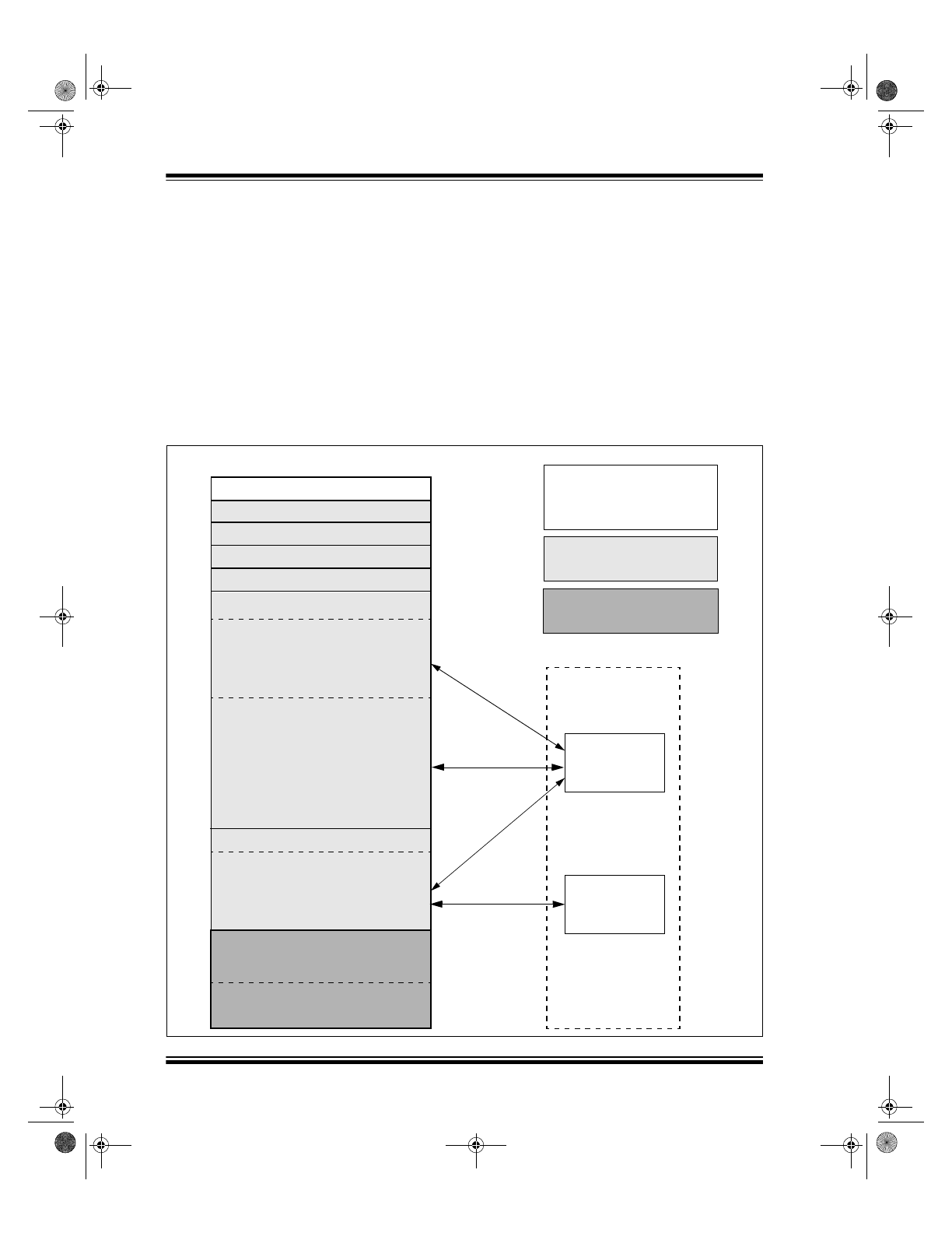
Network Layering Reference
Model
Figure 2-5
shows the ISO Network Layering Reference
Model. The shaded areas are implemented by the
MCP2150, the cross-hatched area is implemented by
an infrared transceiver. The unshaded areas should be
implemented by the Host Controller.
FIGURE 2-5:
ISO REFERENCE LAYER MODEL
OSI REFERENCE LAYERS
Application
Presentation
Session
Transport
Network
Data Link Layer
LLC (Logical Link Control)
Acceptance Filtering
Overload Notification
Recovery Management
MAC (Medium Access Control)
Data Encapsulation/Decapsulation
Frame Coding (stuffing, destuffing)
Medium Access Management
Error Detection
Error Signalling
Acknowledgment
Serialization/Deserialization
Physical Layer
PLS (Physical Signalling)
Bit Encoding/Decoding
Bit Timing
Synchronization
PMA (Physical Medium Attachment)
Driver/Receiver Characteristics
MDI (Medium Dependent Interface)
Connectors
Fault
confinement
(MAC-LME)
Bus Failure
management
(PLS-LME)
Supervisor
Regions implemented
by the MCP2150
Has to be implemented in Host
Controller firmware
Regions implemented
by the Optical Transceiver logic
(such as a PIC
®
microcontroller)
21655C.book Page 10 Thursday, January 10, 2013 12:57 PM