
2002 Microchip Technology Inc.
DS21526A-page 1
Features
• Extremely Low Supply Current for Longer Battery
Life
• Select Mode
™
Operation: Selectable Output
Voltages for High Design Flexibility
• Very Low Dropout Voltage
• 29
µ
V
RMS
Typical Output Noise
• 10
µ
sec (Typ.) Wake-Up Time from SHDN
• 150mA Output Current per Output
• High Output Voltage Accuracy
• Power-Saving Shutdown Mode
• RESET Output Can Be Used as a Low Battery
Detector or Processor Reset Generator
• Over Current Protection and Over Temperature
Shutdown
• Space Saving 10-Pin MSOP Package
Applications
• Load Partitioning
• Battery Operated Systems
• Portable Computers
• Medical Instruments
• Instrumentation
• Pagers and Cellular/PHS Phones
• Linear Post-Regulator for SMPS
Device Selection Table
NOTE: “R” denotes the suffix for the 2.63V V
DET
threshold.
“D” indicates V
OUT1
= V
OUT2
= 2.5, 2.8, 3.0 (selectable).
Other output voltages are available. Please contact Microchip
Technology Inc. for details.
Package Type
General Description
The TC1305 combines two CMOS Low Dropout Regu-
lators and a Microprocessor Monitor in a space saving
10-Pin MSOP package. Designed specifically for
battery operated systems, total supply current is
typically 120
µ
A at full load, 20 to 60 times lower than in
bipolar regulators.
The TC1305 features selectable output voltages for
higher design flexibility. The tri-state SELECT input pin
allows the user to select V
OUT1
and V
OUT2
from 3
different values (2.5V, 2.8V and 3.0V).
An active low RESET is asserted when the detected
voltage (V
DET
) falls below the 2.63V reset voltage
threshold. The RESET output remains low for 300msec
(typical) after V
DET
rises above reset threshold. When
the shutdown controls (SHDN1 and SHDN2) are low,
the regulator output voltages fall to zero, RESET output
remains valid and supply current is reduced to 20
µ
A
(typ.)
Other key features for the device include ultra low noise
operation, fast response to step changes in load and
very low dropout voltage (typically 150mV at full load).
The device also incorporates both over temperature
and over current protection. Each regulator is stable
with an output capacitor of only 1
µ
F and has a
maximum output current of 150mA. The TC1305 is
featured in a 10-Pin MSOP package with selective
output voltages.
Typical Application
Part Number
Package
Junction
Temperature
Range
TC1305R-DVUN
10-Pin MSOP
-40°C to +85°C
V
IN
V
OUT2
V
OUT1
1
V
DET
Bypass
GND
SELECT
2
3
4
5
10
9
8
7
6
SHDN1
RESET
TC1305
SHDN2
10-Pin MSOP
TC1305
470pF
(Optional)
3.3
µF
3.3
µF
1
2
3
4
5
10
9
8
7
6
V
IN
V
DET
GND
SELECT
SHDN1
V
OUT2
V
OUT1
Bypass
RESET
SHDN2
TC1305
Dual 150mA CMOS LDO With Select Mode
™
Operation,
Shutdown and Independent RESET Output
TC1305
DS21526A-page 2
2002 Microchip Technology Inc.
1.0
ELECTRICAL
CHARACTERISTICS
ABSOLUTE MAXIMUM RATINGS*
Input Voltage .........................................................6.5V
Output Voltage........................... (-0.3V) to (V
IN
+ 0.3V)
Power Dissipation................Internally Limited (Note 7)
Maximum Voltage on Any Pin ......... V
IN
+0.3V to -0.3V
Operating Temperature Range.... -40°C < T
J
< +125°C
Storage Temperature Range .............. -55°C to +150°C
*Stresses above those listed under "Absolute Maximum
Ratings" may cause permanent damage to the device. These
are stress ratings only and functional operation of the device
at these or any other conditions above those indicated in the
operation sections of the specifications is not implied.
Exposure to Absolute Maximum Rating conditions for
extended periods may affect device reliability.
TC1305 ELECTRICAL SPECIFICATIONS
Electrical Characteristics: V
IN
= V
R
+ 1V, I
L
= 100
µ
A, C
L
= 3.3
µ
F, SHDN1 > V
IH
, SHDN2 > V
IH
, T
A
= 25°C, unless otherwise
noted. Boldface type specifications apply for junction temperature of -40°C to +125°C. Applies to both V
OUT1
and V
OUT2
.
Symbol
Parameter
Min
Typ
Max
Units
Test Conditions
V
IN
Input Operating Voltage
2.7
—
6.0
V
Note 1
I
OUT
MAX
Maximum Output Current
150
—
—
mA
Per Channel
V
OUT
Output Voltage (V
OUT1
and V
OUT2
)
V
R
– 2.5% V
R
± 0.5% V
R
+ 2.5%
V
Note 2
TCV
OUT
V
OUT
Temperature Coefficient
—
—
20
40
—
—
ppm/°C Note 3
∆
V
OUT
/
∆
V
IN
Line Regulation
—
0.05
0.35
%
(V
R
+ 1V) < V
IN
< 6V
∆
V
OUT
/V
OUT
Load Regulation
—
0.5
2
%
I
L
= 0.1mA to I
OUT
MAX
(Note 4)
V
IN –
V
OUT
Dropout Voltage
—
2
50
100
150
—
120
240
360
mV
I
L
= 100
µ
A
I
L
= 50mA
I
L
= 100mA
I
L
= 150mA
(Note 5)
I
IN
Supply Current
—
120
160
µ
A
SHDN1, SHDN2 = V
IH
, I
L
= 0
I
INSD
Shutdown Supply Current
—
0.05
0.5
µ
A
SHDN1, SHDN2 = 0V
PSRR
Power Supply Rejection Ratio
—
64
—
dB
F
RE
≤
120Hz
I
OUTSC
Output Short Circuit Current
—
600
—
mA
V
OUT
= 0V
∆
V
OUT
∆
P
D
Thermal Regulation
—
0.04
—
V/W
Notes 6, 7
t
WK
Wake Up Time
(from Shutdown Mode)
—
10
—
µ
sec
V
IN
= 5V
C
IN
= 1
µ
F, C
OUT
= 4.7
µ
F
I
L
= 30mA, (See Figure 4-1)
ts
Settling Time
(from Shutdown Mode)
—
40
—
µ
sec
V
IN
= 5V
C
IN
= 1
µ
F, C
OUT
= 4.7
µ
F
I
L
= 30mA, (See Figure 4-1)
Note 1:
The minimum V
IN
has to meet two conditions: V
IN
≥
2.7 and V
IN
≥
V
R
+ V
DROPOUT
.
2:
V
R
is the regulator output voltage setting. For example: V
R
= 2.5V, 2.8V, 3.0V.
3:
4:
Regulation is measured at a constant junction temperature using low duty cycle pulse testing. Load regulation is tested over a load range from
0.1mA to the maximum specified output current. Changes in output voltage due to heating effects are covered by the thermal regulation
specification.
5:
Dropout voltage is defined as the input to output differential at which the output voltage drops 2% below its nominal value measured at a 1V
differential.
6:
Thermal Regulation is defined as the change in output voltage at a time T after a change in power dissipation is applied, excluding load or
line regulation effects. Specifications are for a current pulse equal to I
L
MAX
at V
IN
= 6V for T = 10 msec.
7:
The maximum allowable power dissipation is a function of ambient temperature, the maximum allowable junction temperature and the
thermal resistance from junction-to-air (i.e., T
A
, T
J
,
θ
JA
). Exceeding the maximum allowable power dissipation causes the device to initiate
thermal shutdown. Please see Section 5.0 Thermal Considerations section of this data sheet for more details.
T
C
V
OUT
= (V
OUT
MAX
– V
OUT
MIN
) x 10
6
V
OUT
x
∆
T
2002 Microchip Technology Inc.
DS21526A-page 3
TC1305
TC1305 ELECTRICAL SPECIFICATIONS (CONTINUED)
Electrical Characteristics: V
IN
= V
R
+ 1V, I
L
= 100
µ
A, C
L
= 3.3
µ
F, SHDN1 > V
IH
, SHDN2 > V
IH
, T
A
= 25°C, unless otherwise noted.
Boldface type specifications apply for junction temperature of -40°C to +125°C. Applies to both V
OUT1
and V
OUT2
.
Symbol
Parameter
Min
Typ
Max
Units
Test Conditions
T
SD
Thermal Shutdown Die
Temperature
—
160
—
°C
∆
T
SD
Thermal Shutdown Hysteresis
—
15
—
°C
eN
Output Noise
—
200
—
nV
√
Hz
I
L
= 100
µ
A, F = 1kHz,
C
OUT1
= C
OUT2
= 4.7
µ
F,
C
BYPASS
= 0.01
µ
F
—
29
—
µ
V
RMS
F = 10Hz to 100kHz
SHDN Input
V
IH
SHDN Input High Threshold
65
—
—
%V
IN
V
IN
= 2.7V to 6.0V
V
IL
SHDN Input Low Threshold
—
—
15
%V
IN
V
IN
= 2.7V to 6.0V
SELECT Input
V
SELH
SELECT Input HIgh Threshold
V
IN
– 0.2
—
—
V
V
IN
= 2.7V to 6.0V
V
SELL
SELECT Input Low Threshold
—
0.2
V
V
IN
= 2.7V to 6.0V
RESET Output
V
DET
V
DET
Voltage Range
1.0
1.2
—
—
6.0
6.0
V
T
A
= 0°C to +70°C
T
A
= -40°C to +125°C
V
TH
Reset Threshold
2.59
2.55
2.63
—
2.66
2.70
V
T
A
= +25°C
T
A
= -40°C to +125°C
I
VDET
Reset Circuit Supply Current
—
20
40
µ
A
RESET = Open
Reset Threshold Tempco
—
30
—
ppm/°C
V
DET
to Reset Delay
—
100
—
µ
sec
V
DET
= V
TH
to (V
TH
– 100mV)
Reset Active Time-out Period
140
300
560
msec
V
OL
RESET Output Voltage Low
—
—
—
—
—
—
0.3
0.4
0.3
V
V
DET
= V
TH
MIN
, I
SINK
= 1.2mA
V
DET
= V
TH
MIN
, I
SINK
= 3.2mA
V
DET
> 1.0V, I
SINK
= 50
µ
A
V
OH
RESET Output Voltage High
0.8 V
DET
V
DET
– 1.5
—
—
—
V
V
DET
> V
TH
MAX
, I
SOURCE
= 500
µ
A
V
DET
> V
TH
MAX
, I
SOURCE
= 800
µ
A
Note 1:
The minimum V
IN
has to meet two conditions: V
IN
≥
2.7 and V
IN
≥
V
R
+ V
DROPOUT
.
2:
V
R
is the regulator output voltage setting. For example: V
R
= 2.5V, 2.8V, 3.0V.
3:
4:
Regulation is measured at a constant junction temperature using low duty cycle pulse testing. Load regulation is tested over a load range from
0.1mA to the maximum specified output current. Changes in output voltage due to heating effects are covered by the thermal regulation
specification.
5:
Dropout voltage is defined as the input to output differential at which the output voltage drops 2% below its nominal value measured at a 1V
differential.
6:
Thermal Regulation is defined as the change in output voltage at a time T after a change in power dissipation is applied, excluding load or
line regulation effects. Specifications are for a current pulse equal to I
L
MAX
at V
IN
= 6V for T = 10 msec.
7:
The maximum allowable power dissipation is a function of ambient temperature, the maximum allowable junction temperature and the
thermal resistance from junction-to-air (i.e., T
A
, T
J
,
θ
JA
). Exceeding the maximum allowable power dissipation causes the device to initiate
thermal shutdown. Please see Section 5.0 Thermal Considerations section of this data sheet for more details.
T
C
V
OUT
= (V
OUT
MAX
– V
OUT
MIN
) x 10
6
V
OUT
x
∆
T
TC1305
DS21526A-page 4
2002 Microchip Technology Inc.
2.0
PIN DESCRIPTIONS
The descriptions of the pins are listed in Table 2-1.
TABLE 2-1:
PIN FUNCTION TABLE
Pin No.
(10-Pin MSOP)
Symbol
Description
1
V
DET
Detected input voltage. V
DET
and V
IN
can be connected together.
2
V
IN
Power supply input.
3
GND
Ground terminal.
4
SELECT
Tri-state input for setting V
OUT1
and V
OUT2
. SELECT = GND for V
OUT1
= V
OUT2
= 2.5V,
SELECT = V
IN
for V
OUT1
= V
OUT2
= 3.0V and SELECT = No connect for V
OUT1
= V
OUT2
= 2.8V.
5
SHDN1
Shutdown control input for V
OUT1
. Regulator 1 is fully enabled when a logic high is applied to
this input. Regulator 1 enters shutdown when a logic low is applied to this input. During
shutdown, regulator output voltage falls to zero, RESET output remains valid.
6
SHDN2
Shutdown control input for V
OUT2
. Regulator 2 is fully enabled when a logic high is applied to
this input. Regulator 2 enters shutdown when a logic low is applied to this input. During
shutdown, regulator output voltage falls to zero, RESET output remains valid.
7
Bypass
Reference bypass input. Connecting a 0.01
µ
F to this input further reduces output noise.
8
V
OUT1
Regulated voltage output 1.
9
V
OUT2
Regulated voltage output 2.
10
RESET
RESET Output. RESET = Low when V
DET
is below the Reset Threshold Voltage.
RESET = High when V
DET
is above the Reset Threshold Voltage.

2002 Microchip Technology Inc.
DS21526A-page 5
TC1305
3.0
DETAILED DESCRIPTION
The TC1305 is a precision fixed output voltage
regulator that contains two fully independent 150mA
regulator outputs. The device
features separate
shutdown modes for low-power operation, and a
common bypass pin that can be used to further reduce
output noise. The Select Mode
™
operation allows the
user to select V
OUT1
and V
OUT2
from three different
values (2.5V, 2.8V, 3.0V), therefore providing high
design flexibility. The CMOS construction of the
TC1305 results to a very low supply current, which
does not increase with load changes. In addition, V
OUT
remains stable and within regulation at no load
currents.
The TC1305 also features an integrated microproces-
sor supervisor that monitors power-up, power-down,
and brown-out conditions. The active low RESET
signal is asserted when the detected voltage V
DET
falls
below the reset voltage threshold (2.63V). The RESET
output remains low for 300msec (typical) after V
DET
rises above the reset threshold. The RESET output of
the TC1305 is ensured valid down to V
DET
= 1V and is
optimized to reject fast transient glitches on the
monitored power supply line.
4.0
TYPICAL APPLICATIONS
4.1
Input and Output Capacitor
The TC1305 is stable with a wide range of capacitor
values and types. A capacitor with a minimum value of
1
µ
F from V
OUT
to Ground is required. The output
capacitor should have an effective series resistance
(ESR) of 0.1
Ω
to 10
Ω
for a 1
µ
F capacitor and 0.01
Ω
to
10
Ω
for a 10
µ
F capacitor. A 1
µ
F capacitor should be
connected from the V
IN
to GND if there is more than 10
inches of wire between the regulator and the AC filter
capacitor, or if a battery is used as the power source.
Aluminum electrolytic or tantalum capacitor types can
be used. (Since many aluminum electrolytic capacitors
freeze at approximately -30°C, solid tantalums are
recommended for applications operating below -20°C).
When operating from sources other than batteries,
supply-noise rejection and transient response can be
improved by increasing the value of the input and
output capacitors and employing passive filtering
techniques.
4.2
Bypass Capacitor
A 0.01
µ
F capacitor connected from the bypass input to
ground
reduces
noise
present
on
the
internal
reference, which in turn significantly reduces output
noise. If output noise is not a concern, this input may be
left unconnected.
Larger capacitor values may be used, but result in a
longer time period to rated output voltage when power
is initially applied.
4.3
Shutdown Mode
Applying a logic high to each of the shutdown pins turns
on the corresponding output. Each regulator enters
shutdown mode when a logic low is applied in the
corresponding input. During shutdown mode, the out-
put voltage falls to zero, and regulator supply current is
reduced to 0.5
µ
A (max). If shutdown mode is not
necessary, the pins should be connected to V
IN
.
TC1305
DS21526A-page 6
2002 Microchip Technology Inc.
4.4
Select Mode
™
Operation
The Select Mode
™
operation is a tri-state input that
allows the user to select V
OUT1
and V
OUT2
from three
different values. By connecting the SELECT pin to
GND, both output voltages (V
OUT1
, V
OUT2
) supply
2.5V. Connecting the SELECT pin to V
IN
results in both
output channels supplying a fixed 3.0V output. Last but
not least, leaving the SELECT pin floating sets both
voltages to 2.8V. This output voltage functionality
provides high design flexibility and minimizes costs
associated with inventory, time-to-market and new
device qualifications.
4.5
RESET Output
The microprocessor supervisor of theTC1305 provides
accurate supply voltage monitoring and reset timing
during power-up, power-down and brown-out condi-
tions. The RESET output is valid to V
DET
= 1.0V (below
this point it becomes an open circuit and does not sink
current) and is able to reject negative going transients
(glitches) on the power supply line. Transient immunity
can further be improved by adding a capacitor close to
the V
DET
pin of the TC1305.
4.6
Turn On Response
The turn on response is defined as two separate
response categories, Wake Up Time (t
WK
) and Settling
Time (t
S
).
The TC1305 has a fast Wake Up Time (10
µ
sec typical)
when released from shutdown. See Figure 4-1 for the
Wake Up Time designated as t
WK
. The Wake Up Time
is defined as the time it takes for the output to rise to 2%
of the V
OUT
value after being released from shutdown.
The total turn on response is defined as the Settling
Time (t
S
), see Figure 4-1. Settling Time (inclusive with
t
WK
) is defined as the condition when the output is
within 2% of its fully enabled value (40
µ
sec typical)
when released from shutdown. The settling time of the
output voltage is dependent on load conditions and
output capacitance on V
OUT
(RC response).
FIGURE 4-1:
WAKE-UP RESPONSE
TIME
V
IH
t
S
t
WK
V
OUT
98%
2%
V
IL
SHDN
2002 Microchip Technology Inc.
DS21526A-page 7
TC1305
5.0
THERMAL CONSIDERATIONS
5.1
Thermal Shutdown
Integrated
thermal
protection
circuitry
shuts
the
regulator off when die exceeds approximately 160°C.
The regulator remains off until the die temperature
drops to approximately 145°C.
Thermal shutdown is intended to protect the device
under transient accidental (fault) overload conditions.
Thermal Shutdown may not protect the LDO while
operating above junction temperatures of 125°C
continuously. Sufficient thermal evaluation of the
design needs to be conducted to ensure that the
junction temperature does not exceed 125°C.
5.2
Power Dissipation
The amount of power the regulator dissipates is
primarily a function of input and output voltage, and
output current. The following equation is used to
calculate worst case actual power dissipation.
EQUATION 5-1:
The
maximum
allowable
power
dissipation
(Equation 5-2) is a function of the maximum ambient
temperature (T
A
MAX
), the maximum allowable die
temperature (125°C), and the thermal resistance from
junction-to-air (
θ
JA
). The MSOP-10 package has a
θ
JA
of approximately 113°C/W when mounted on a four
layer FR4 dielectric copper clad PC board.
EQUATION 5-2:
Equation 5-1
can
be
used
in
conjunction
with
Equation 5-2 to ensure regulator thermal operation is
within limits. For example:
Given:
V
IN
MAX
= 3.8V ± 5%
V
OUT1
MIN
= 3.0V ± 2.5%
V
OUT2
MIN
= 3.0V ± 2.5%
I
LOAD1
MAX
= 120mA
I
LOAD2
MAX
= 120mA
T
J
MAX
= 125°C
T
A
MAX
= 55°C
θ
JA
= 113°C/W
Find: 1. Actual power dissipation
2. Maximum allowable dissipation
Actual power dissipation:
P
D
≈
[(V
IN
MAX
– V
OUT1
MIN
)] x I
LOAD1
MAX
+ [(V
IN
MAX
– V
OUT2
MIN
)] x I
LOAD2
MAX
[(3.8 x 1.05) – (3.0 x .975)] x 120 x 10
-3
+ [(3.8 x 1.05) – (3.0 x .975)] x 120 x 10
-3
= 256mW
Maximum allowable power dissipation:
In this example, the TC1305 dissipates a maximum of
256mW; below the allowable limit of 620mW. In a
similar manner, Equation 5-1 and Equation 5-2 can be
used to calculate maximum current and/or input
voltage limits. For example, the maximum allowable
V
IN
is found by substituting the maximum allowable
power dissipation of 620mW into Equation 5-1, from
which V
IN
MAX
= 5.6V.
5.3
Layout Considerations
The primary path of heat conduction out of the package
is via the package leads. Therefore, layouts having a
ground plane, wide traces at the pads, and wide power
supply bus lines combine to lower
θ
JA
and therefore
increase the maximum allowable power dissipation
limit.
Where:
P
D
≈
(V
IN
MAX
– V
OUT1
MIN
)I
LOAD1
MAX
+
P
D
V
IN
MAX
V
OUT1
MIN
I
LOAD1
MAX
= Worst case actual power dissipation
= Minimum regulator output voltage1
= Maximum output (load) current1
= Maximum voltage on V
IN
(V
IN
MAX
– V
OUT2
MIN
)I
LOAD2
MAX
V
OUT2
MIN
I
LOAD2
MAX
= Minimum regulator output voltage2
= Maximum output (load) current2
P
D
MAX
= (T
J
MAX
– T
A
MAX
)
θ
JA
Where all terms are previously defined.
P
D
= (T
J
MAX
– T
A
MAX
)
θ
JA
= (125 – 55)
113
= 620mW
TC1305
DS21526A-page 8
2002 Microchip Technology Inc.
6.0
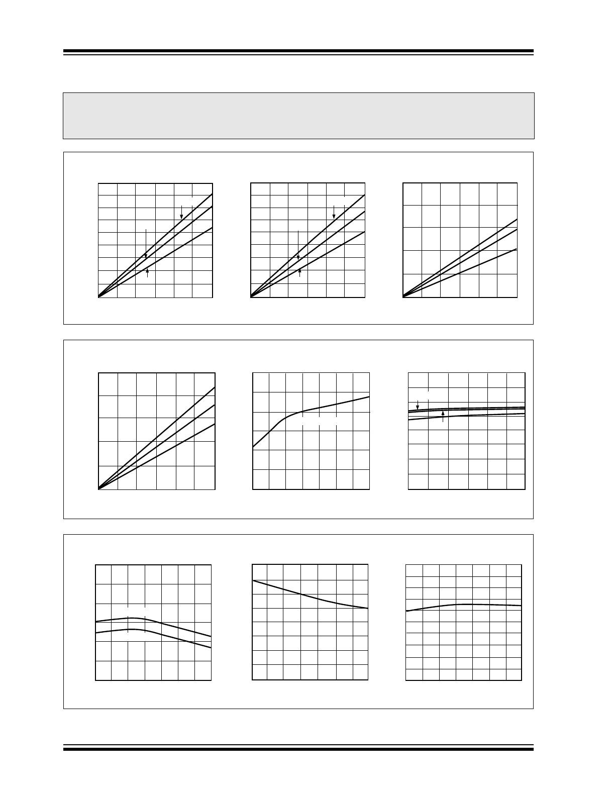
TYPICAL CHARACTERISTICS
Note:
The graphs and tables provided following this note are a statistical summary based on a limited number of
samples and are provided for informational purposes only. The performance characteristics listed herein are
not tested or guaranteed. In some graphs or tables, the data presented may be outside the specified
operating range (e.g., outside specified power supply range) and therefore outside the warranted range.
0 25 50 75 100 125 150
0 25 50 75 100 125 150
0.18
0.16
0.14
0.12
0.10
0.08
0.06
0.04
0.02
0.00
DROPOUT VOLTAGE (V)
Dropout Voltage1 vs. Load Current
(SELECT = NC)
LOAD CURRENT (mA)
LOAD CURRENT (mA)
-45
°C
25
°C
130
°C
0.18
0.16
0.14
0.12
0.10
0.08
0.06
0.04
0.02
0.00
DROPOUT VOLTAGE (V)
Dropout Voltage1 vs. Load Current
(SELECT = V
DD
)
-45
°C
25
°C
0 25 50 75 100 125 150
LOAD CURRENT (mA)
DROPOUT VOLTAGE (V)
Dropout Voltage2 vs. Load Current
(SELECT = V
DD
)
-45
°C
25
°C
0.25
0.20
0.15
0.10
0.05
0.00
130
°C
130
°C
130
°C
-45 -20 5 30 55 80 105 130
3 3.5 4 4.5 5 5.5 6
Load Regulation
vs. Temperature
TEMPERATURE (
°C)
I
L
= 0.1 to 150mA
LOAD REGULATION (%)
0.600
0.500
0.400
0.300
0.200
0.100
0.000
I
DD
vs. V
DD
(SELECT = GND)
V
DD
(V)
I DD
(µ
A)
150
0 25 50 75 100 125 150
LOAD CURRENT (mA)
DROPOUT VOLTAGE (V)
Dropout Voltage2 vs. Load Current
(SELECT = V
DD
)
-45
°C
25
°C
0.25
0.20
0.15
0.10
0.05
0.00
140
120
100
80
60
40
20
0
-45
°C 25°C
130
°C
-40 -20 5 30 55 80 105 125
2.70
2.68
2.66
2.64
2.62
2.60
2.58
2.56
2.54
2.52
2.50
V
CC
TRIP POINT (V)
V
CC
Trip Point vs.
Temperature (
°C)
TEMPERATURE (
°C)
TEMPERATURE (
°C)
130
100
-40 -20 5 30 55 80 105 125
V
DD
= 6.0V
V
DD
= 3.0V
I
DD
vs. Temperature
(SELECT = NC)
TEMPERATURE (
°C)
I
DD
(
µ
A)
140
120
110
90
80
-40 -20 5 30 55 80 105 125
400
350
300
250
200
150
100
50
0
RESET TIMING (
µ
sec)
Reset Active Time vs.
Temperature (
°C)
2002 Microchip Technology Inc.
DS21526A-page 9
TC1305
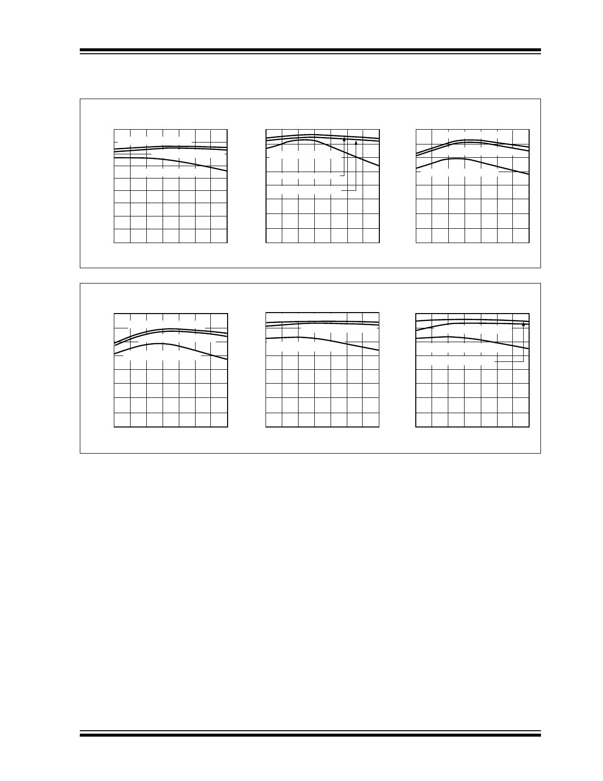
6.0
TYPICAL CHARACTERISTICS (CONTINUED)
-45 -20 5 30 55 80 105 130
3.01
3.00
2.99
2.98
2.97
2.96
2.95
2.94
2.93
2.92
V
OUT1
vs. Temperature
(SELECT = V
DD
)
TEMPERATURE (
°C)
V
DD
= 6.0V & I
L
= 100
µA
V
DD
= 4.0V & I
L
= 100
µA
3.00
2.99
2.98
2.97
2.96
2.95
2.94
2.93
2.92
V
OUT1
(V)
-45 -20 5 30 55 80 105 130
V
OUT2
vs. Temperature
(SELECT = V
DD
)
TEMPERATURE (
°C)
V
OUT2
(V)
V
DD
= 3.8V & I
L
= 150mA
V
DD
= 4.0V & I
L
= 100
µA
V
DD
= 6.0V & I
L
= 100
µA
2.81
2.80
2.79
2.78
2.77
2.76
2.75
2.74
2.73
-45 -20 5 30 55 80 105 130
V
OUT1
vs. Temperature
(SELECT = NC)
TEMPERATURE (
°C)
V
OUT1
(V)
V
DD
= 6.0V & I
L
= 100
µA
V
DD
= 3.8V & I
L
= 150mA
V
DD
= 3.8V & I
L
= 100mA
V
DD
= 3.8V & I
L
= 100mA
2.81
2.80
2.79
2.78
2.77
2.76
2.75
2.74
2.73
-45 -20 5 30 55 80 105 130
V
OUT2
vs. Temperature
(SELECT = NC)
TEMPERATURE (
°C)
V
OUT2
(V)
V
DD
= 3.8V & I
L
= 150mA
V
DD
= 6.0V & I
L
= 100
µA
V
DD
= 6.0V & I
L
= 100
µA
2.51
2.50
2.49
2.48
2.47
2.46
2.45
2.44
2.43
-45 -20 5 30 55 80 105 130
V
OUT1
vs. Temperature
(SELECT = GND)
TEMPERATURE (
°C)
V
OUT1
(V)
V
DD
= 3.5V & I
L
= 100
µA
V
DD
= 3.5V & I
L
= 150mA
V
DD
= 6.0V & I
L
= 100
µA
2.51
2.50
2.49
2.48
2.47
2.46
2.45
2.44
2.43
-45 -20 5 30 55 80 105 130
V
OUT2
vs. Temperature
(SELECT = GND)
TEMPERATURE (
°C)
V
OUT2
(V)
V
DD
= 3.5V & I
L
= 100
µA
V
DD
= 3.5V & I
L
= 150mA
V
DD
= 6.0V & I
L
= 100µA
TC1305
DS21526A-page 10
2002 Microchip Technology Inc.
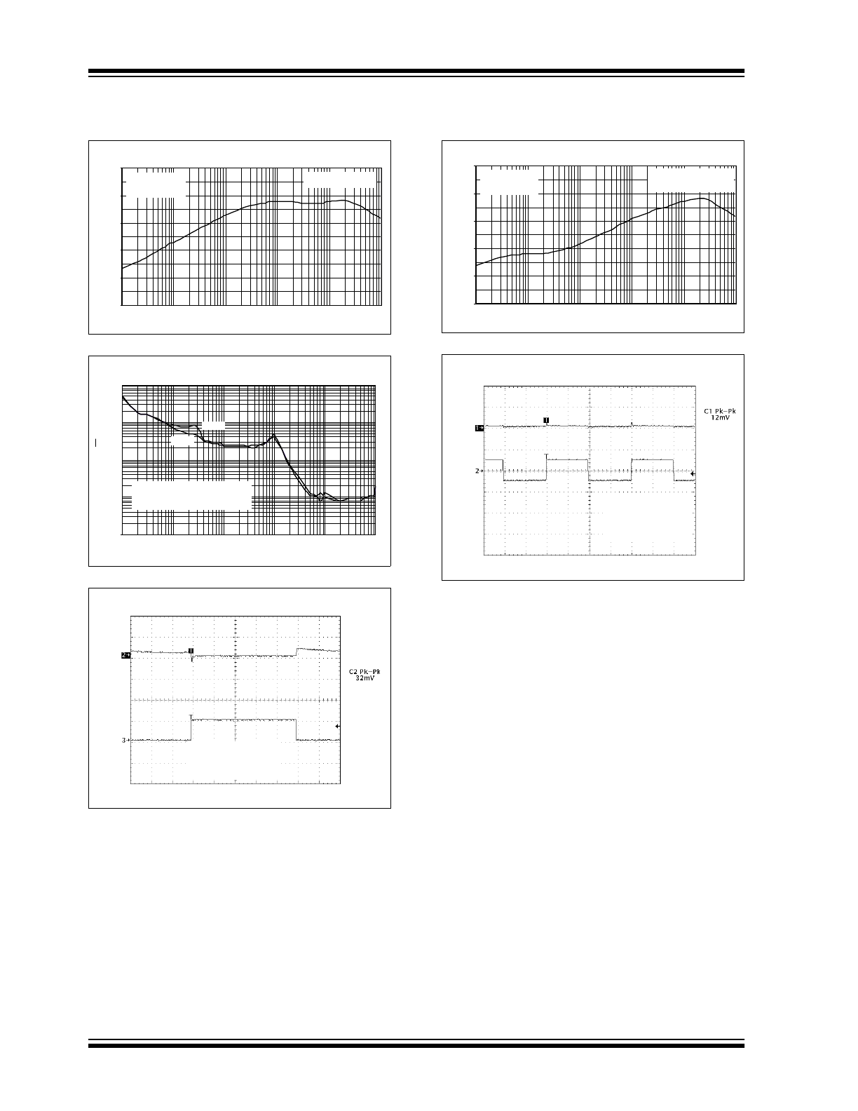
6.0
TYPICAL CHARACTERISTICS (CONTINUED)
-100
-80
-60
-40
-20
0
f (Hz)
I
OUT
= 150mA
C
OUT
= 10
µF Tantalum
V
INDC
= 4V
V
INAC
= 100mV
P-P
V
OUTDC
= 3V
10
100
1k
10k
100k
1M
PSRR (dB)
Power Supply Rejection Ratio vs. Frequency
10
1
0.1
0.001
0.01
Frequency (kHz)
0.01
0.1
1
10
1000
100
Noise (mV/
√
HZ)
V
OUT2
C
OUT1
= C
OUT2
= 4.7
µF,
C
BYPASS
= 0.01
µF, I
LOAD
= 100
µA,
V
IN
= 4.0V, V
OUT1
= V
OUT2
= 3.0V
V
OUT1
Output Noise
150mA
100
µA
Output Voltage
(50mV / div)
Output Current
Time (100ms / div)
V
IN
= 4V
V
OUT
= 3V
C
OUT
= 10
µF Ceramic
C
BYP
= 0.01
µF
Load Transient Response
-100
-80
-60
-40
-20
0
f (Hz)
10
100
1k
10k
100k
1M
PSRR (dB)
I
OUT
= 150mA
C
OUT
= 10
µF Tantalum
C
BYPASS
= 0.01
µF Ceramic
V
INDC
= 4V
V
INAC
= 100mV
P-P
V
OUTDC
= 3V
Power Supply Rejection Ratio vs. Frequency
6V
4V
Line Transient Response
Output Voltage
(50mV / div)
Input Voltage
2V / div
Time (2
µs / div)
C
OUT
= 10
µF Ceramic
C
IN
= 0
C
BYP
= 0.01
µF
I
LOAD
= 100
µA
V
OUT
= 3V