
© 2007 Microchip Technology Inc.
DS21483D-page 1
TC9400/9401/9402
Features:
VOLTAGE-TO-FREQUENCY
• Choice of Linearity:
- TC9401: 0.01%
- TC9400: 0.05%
- TC9402: 0.25%
• DC to 100 kHz (F/V) or 1 Hz to 100 kHz (V/F)
• Low Power Dissipation: 27 mW (Typ.)
• Single/Dual Supply Operation:
- +8V to +15V or ±4V to ±7.5V
• Gain Temperature Stability: ±25 ppm/°C (Typ.)
• Programmable Scale Factor
FREQUENCY-TO-VOLTAGE
• Operation: DC to 100 kHz
• Choice of Linearity:
- TC9401: 0.02%
- TC9400: 0.05%
- TC9402: 0.25%
• Programmable Scale Factor
Applications:
• Microprocessor Data Acquisition
• 13-bit Analog-to-Digital Converters (ADC)
• Analog Data Transmission and Recording
• Phase Locked Loops
• Frequency Meters/Tachometer
• Motor Control
• FM Demodulation
General Description:
The TC9400/9401/9402 are low-cost Voltage-to-Fre-
quency (V/F) converters, utilizing low-power CMOS
technology. The converters accept a variable analog
input signal and generate an output pulse train, whose
frequency is linearly proportional to the input voltage.
The devices can also be used as highly accurate
Frequency-to-Voltage (F/V) converters, accepting
virtually any input frequency waveform and providing a
linearly proportional voltage output.
A complete V/F or F/V system only requires the
addition of two capacitors, three resistors, and refer-
ence voltage.
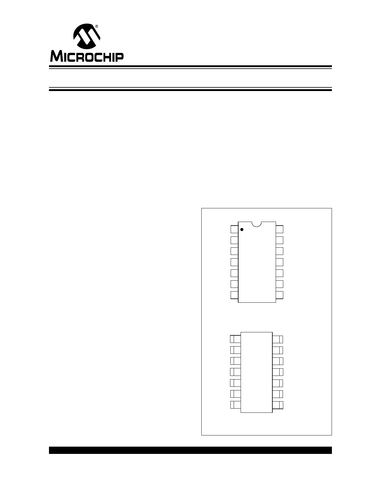
Package Type
1
2
3
4
5
6
7
14
13
12
11
10
9
8
V
DD
NC
AMPLIFIER OUT
THRESHOLD
DETECTOR
FREQ/2 OUT
OUTPUT COMMON
PULSE FREQ OUT
I
BIAS
ZERO ADJ
I
IN
V
SS
V
REF
OUT
GND
V
REF
1
2
3
4
5
6
7
14
13
12
11
10
9
8
TC9400
TC9401
TC9402
14-Pin Plastic DIP/CERDIP
14-Pin SOIC
TC9400
TC9401
TC9402
NC = No Internal Connection
V
DD
NC
AMPLIFIER OUT
THRESHOLD
DETECTOR
FREQ/2 OUT
OUTPUT COMMON
PULSE FREQ OUT
I
BIAS
ZERO ADJ
I
IN
V
SS
V
REF
OUT
GND
V
REF
Voltage-to-Frequency / Frequency-to-Voltage Converters
TC9400/9401/9402
DS21483D-page 2
© 2007 Microchip Technology Inc.
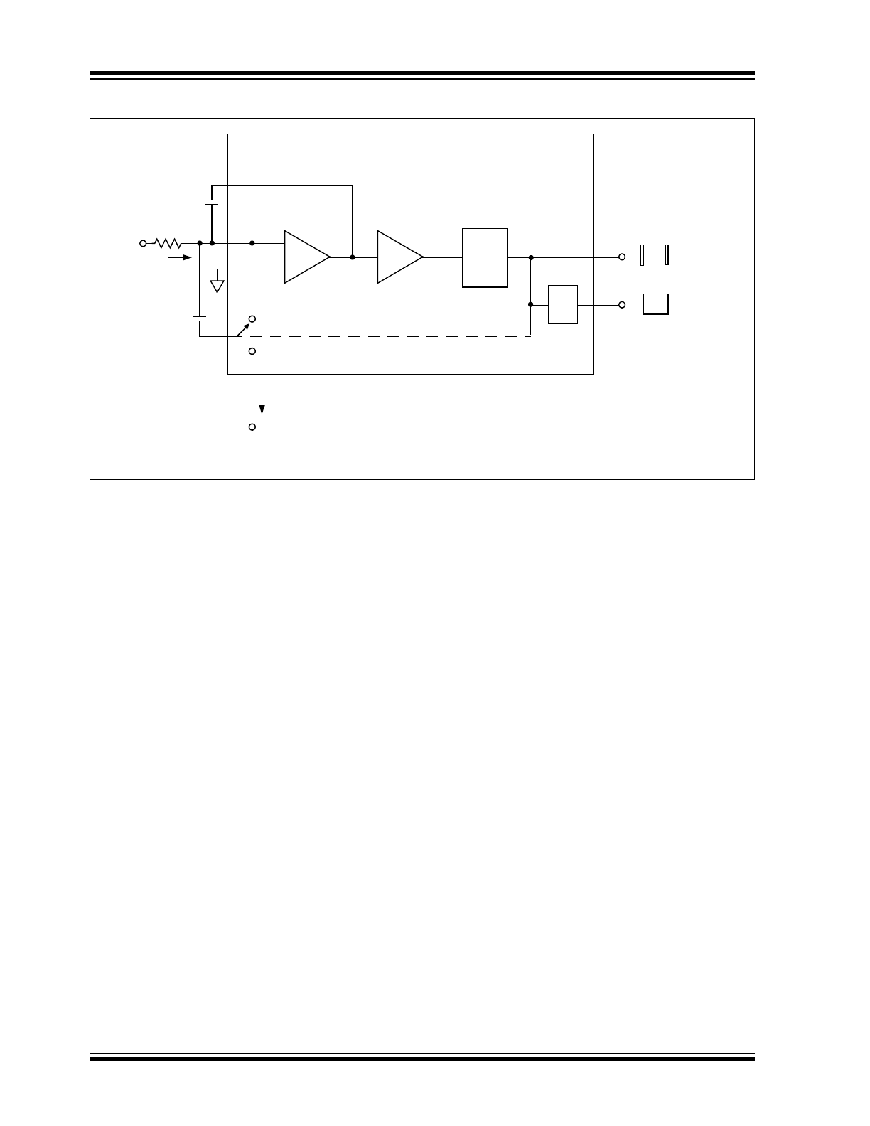
Functional Block Diagram
IIN
IREF
TC9400
RIN
Integrator
Op Amp
Integrator
Capacitor
Threshold
Detector
One
Shot
Pulse Output
Pulse/2 Output
÷
2
Input
Voltage
Reference
Capacitor
Reference
Voltage
© 2007 Microchip Technology Inc.
DS21483D-page 3
TC9400/9401/9402
1.0
ELECTRICAL
CHARACTERISTICS
Absolute Maximum Ratings †
V
DD
– V
SS
......................................................................+18V
I
IN
..................................................................................10 mA
V
OUT
MAX
– V
OUT
Common.................................................23V
V
REF
– V
SS
.....................................................................-1.5V
Storage Temperature Range.........................-65°C to +150°C
Operating Temperature Range:
C Device ...................................................... 0°C to +70°C
E Device....................................................-40°C to +85°C
Package Dissipation (T
A
≤ 70°C):
8-Pin CerDIP........................................................800 mW
8-Pin Plastic DIP ..................................................730 mW
8-Pin SOIC...........................................................470 mW
†
Stresses above those listed under “Absolute Maximum
Ratings” may cause permanent damage to the device. These
are stress ratings only and functional operation of the device
at these or any other conditions above those indicated in the
operation sections of the specifications is not implied.
Exposure to Absolute Maximum Rating conditions for
extended periods may affect device reliability.
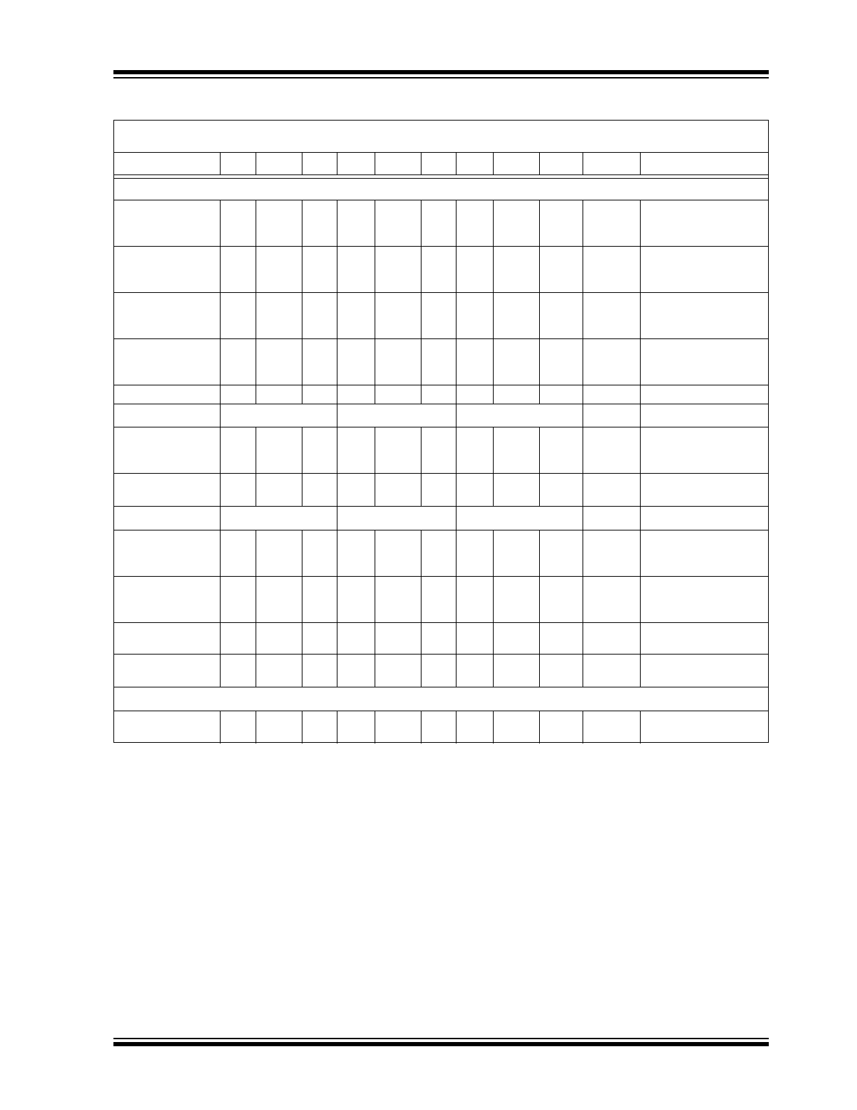
TC940X ELECTRICAL SPECIFICATIONS
Electrical Characteristics: unless otherwise specified, V
DD
= +5V, V
SS
= -5V, V
GND
= 0V, V
REF
= -5V, R
BIAS
= 100 k
Ω, Full Scale =
10 kHz. T
A
= +25°C, unless temperature range is specified (-40°C to +85°C for E device, 0°C to +70°C for C device).
Parameter
Min
Typ
Max
Min
Typ
Max
Min
Typ
Max
Units
Test Conditions
Voltage-to-Frequency
Accuracy
TC9400
TC9401
TC9402
Linearity 10 kHz
—
0.01
0.05
—
0.004
0.01
—
0.05
0.25
%
Full Scale
Output Deviation from
Straight Line Between
Normalized Zero and
Full Scale Input
Linearity 100 kHz
—
0.1
0.25
—
0.04
0.08
—
0.25
0.5
%
Full Scale
Output Deviation from
Straight Line Between
Normalized Zero Read-
ing and Full Scale Input
Gain Temperature
Drift (Note 1)
—
±25
±40
—
±25
±40
—
±50
± 100 ppm/°C
Full Scale
Variation in Gain A due
to Temperature Change
Gain Variance
—
±10
—
—
±10
—
—
±10
—
% of
Nominal
Variation from Ideal
Accuracy
Zero Offset
(Note 2)
—
±10
±50
—
±10
±50
—
±20
±100
mV
Correction at Zero
Adjust for Zero Output
when Input is Zero
Zero Temperature
Drift (Note 1)
—
±25
±50
—
±25
±50
—
±50
±100
µV/°C
Variation in Zero Offset
Due to Temperature
Change
Note 1: Full temperature range; not tested.
2: I
IN
= 0.
3: Full temperature range, I
OUT
= 10 mA.
4: I
OUT
= 10 µA.
5: Threshold Detect = 5V, Amp Out = 0V, full temperature range.
6: 10 Hz to 100 kHz; not tested.
7: 5 µs minimum positive pulse width and 0.5 µs minimum negative pulse width.
8: t
R
= t
F
= 20 ns.
9: R
L
≥ 2 kΩ, tested @ 10 kΩ.
10: Full temperature range, V
IN
= -0.1V.
TC9400/9401/9402
DS21483D-page 4
© 2007 Microchip Technology Inc.
Analog Input
I
IN
Full Scale
—
10
—
—
10
—
—
10
—
µA
Full Scale Analog Input
Current to achieve
Specified Accuracy
I
IN
Over Range
—
—
50
—
—
50
—
—
50
µA
Over Range Current
Response Time
—
2
—
—
2
—
—
2
—
Cycle
Settling Time to 0.1%
Full Scale
Digital Section
TC9400
TC9401
TC9402
V
SAT
@ I
OL
= 10mA
—
0.2
0.4
—
0.2
0.4
—
0.2
0.4
V
Logic “0” Output
Voltage (Note 3)
V
OUT
MAX
– V
OUT
Common (Note 4)
—
—
18
—
—
18
—
—
18
V
Voltage Range Between
Output and Common
Pulse Frequency
Output Width
—
3
—
—
3
—
—
3
—
µs
Frequency-to-Voltage
Supply Current
I
DD
Quiescent
(Note 5)
—
1.5
6
—
1.5
6
—
3
10
mA
Current Required from
Positive Supply during
Operation
I
SS
Quiescent
(Note 5)
—
-1.5
-6
—
-1.5
-6
—
-3
-10
mA
Current Required from
Negative Supply during
Operation
V
DD
Supply
4
—
7.5
4
—
7.5
4
—
7.5
V
Operating Range of
Positive Supply
V
SS
Supply
-4
—
-7.5
-4
—
-7.5
-4
—
-7.5
V
Operating Range of
Negative Supply
Reference Voltage
V
REF
– V
SS
-2.5
—
—
-2.5
—
—
-2.5
—
—
V
Range of Voltage
Reference Input
Accuracy
Non-Linearity
(Note 10)
—
0.02
0.05
—
0.01
0.02
—
0.05
0.25
%
Full Scale
Deviation from ideal
Transfer Function as a
Percentage Full Scale
Voltage
Input Frequency
Range
(Notes 7 and 8)
10
—
100k
10
—
100k
10
—
100k
Hz
Frequency Range for
Specified Non-Linearity
TC940X ELECTRICAL SPECIFICATIONS (CONTINUED)
Electrical Characteristics: unless otherwise specified, V
DD
= +5V, V
SS
= -5V, V
GND
= 0V, V
REF
= -5V, R
BIAS
= 100 k
Ω, Full Scale =
10 kHz. T
A
= +25°C, unless temperature range is specified (-40°C to +85°C for E device, 0°C to +70°C for C device).
Parameter
Min
Typ
Max
Min
Typ
Max
Min
Typ
Max
Units
Test Conditions
Note 1: Full temperature range; not tested.
2: I
IN
= 0.
3: Full temperature range, I
OUT
= 10 mA.
4: I
OUT
= 10 µA.
5: Threshold Detect = 5V, Amp Out = 0V, full temperature range.
6: 10 Hz to 100 kHz; not tested.
7: 5 µs minimum positive pulse width and 0.5 µs minimum negative pulse width.
8: t
R
= t
F
= 20 ns.
9: R
L
≥ 2 kΩ, tested @ 10 kΩ.
10: Full temperature range, V
IN
= -0.1V.
© 2007 Microchip Technology Inc.
DS21483D-page 5
TC9400/9401/9402
Frequency Input
Positive Excursion
0.4
—
V
DD
0.4
—
V
DD
0.4
—
V
DD
V
Voltage Required to
Turn Threshold
Detector On
Negative Excursion
-0.4
-2
-0.4
—
-2
-0.4
—
-2
V
Voltage Required to
Turn Threshold
Detector Off
Minimum Positive
Pulse Width
(Note 8)
—
5
—
—
5
—
—
5
—
μs
Time between
Threshold Crossings
Minimum Negative
Pulse Width
(Note 8)
—
0.5
—
—
0.5
—
—
0.5
—
μs
Time Between
Threshold Crossings
Input Impedance
—
10
—
—
10
—
—
10
M
Ω
Analog Outputs
TC9400
TC9401
TC9402
Output Voltage
(Note 9)
—
V
DD
– 1
—
—
V
DD
– 1
—
—
V
DD
– 1
—
V
Voltage Range of Op
Amp Output for
Specified Non-Linearity
Output Loading
2
—
—
2
—
—
2
—
—
k
Ω
Resistive Loading at
Output of Op Amp
Supply Current
TC9400
TC9401
TC9402
I
DD
Quiescent
(Note 10)
—
1.5
6
—
1.5
6
—
3
10
mA
Current Required from
Positive Supply During
Operation
I
SS
Quiescent
(Note 10)
—
-1.5
-6
-1.5
-6
—
-3
-10
mA
Current Required from
Negative Supply During
Operation
V
DD
Supply
4
—
7.5
4
—
7.5
4
—
7.5
V
Operating Range of
Positive Supply
V
SS
Supply
-4
—
-7.5
-4
—
-7.5
-4
—
-7.5
V
Operating Range of
Negative Supply
Reference Voltage
V
REF
– V
SS
-2.5
—
—
-2.5
—
—
-2.5
—
—
V
Range of Voltage
Reference Input
TC940X ELECTRICAL SPECIFICATIONS (CONTINUED)
Electrical Characteristics: unless otherwise specified, V
DD
= +5V, V
SS
= -5V, V
GND
= 0V, V
REF
= -5V, R
BIAS
= 100 k
Ω, Full Scale =
10 kHz. T
A
= +25°C, unless temperature range is specified (-40°C to +85°C for E device, 0°C to +70°C for C device).
Parameter
Min
Typ
Max
Min
Typ
Max
Min
Typ
Max
Units
Test Conditions
Note 1: Full temperature range; not tested.
2: I
IN
= 0.
3: Full temperature range, I
OUT
= 10 mA.
4: I
OUT
= 10 µA.
5: Threshold Detect = 5V, Amp Out = 0V, full temperature range.
6: 10 Hz to 100 kHz; not tested.
7: 5 µs minimum positive pulse width and 0.5 µs minimum negative pulse width.
8: t
R
= t
F
= 20 ns.
9: R
L
≥ 2 kΩ, tested @ 10 kΩ.
10: Full temperature range, V
IN
= -0.1V.
TC9400/9401/9402
DS21483D-page 6
© 2007 Microchip Technology Inc.
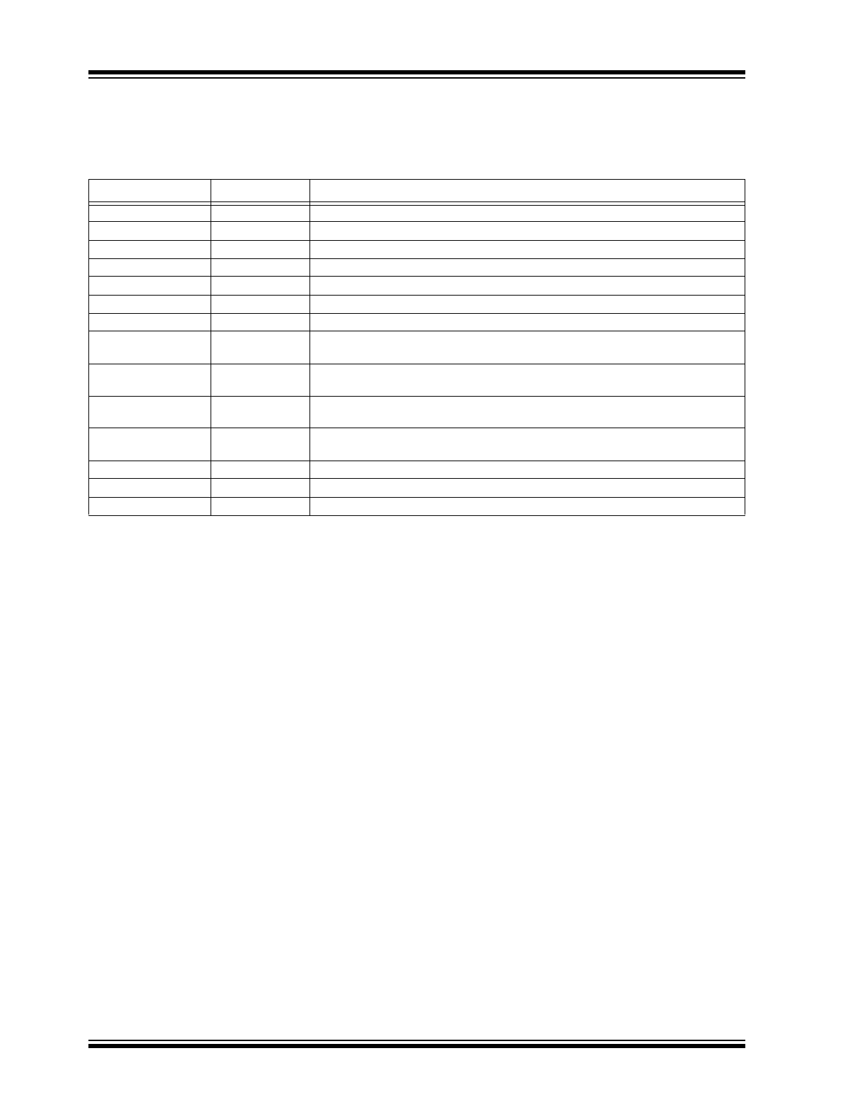
2.0
PIN DESCRIPTIONS
The descriptions of the pins are listed in
Table 2-1
.
TABLE 2-1:
PIN FUNCTION TABLE
2.1
Bias Current (I
BIAS
)
An external resistor, connected to V
SS
, sets the bias
point for the TC9400. Specifications for the TC9400 are
based on R
BIAS
= 100 k
Ω ±10%, unless otherwise
noted.
Increasing the maximum frequency of the TC9400
beyond 100 kHz is limited by the pulse width of the
pulse output (typically 3 µs). Reducing R
BIAS
will
decrease the pulse width and increase the maximum
operating frequency, but linearity errors will also
increase. R
BIAS
can be reduced to 20 k
Ω, which will
typically produce a maximum full scale frequency of
500 kHz.
2.2
Zero Adjust
This pin is the non-inverting input of the operational
amplifier. The low frequency set point is determined by
adjusting the voltage at this pin.
2.3
Input Current (I
IN
)
The inverting input of the operational amplifier and the
summing junction when connected in the V/F mode. An
input current of 10
μA is specified, but an over range
current up to 50
μA can be used without detrimental
effect to the circuit operation. I
IN
connects the summing
junction of an operational amplifier. Voltage sources
cannot be attached directly, but must be buffered by
external resistors.
2.4
Voltage Capacitor (V
REF
Out)
The charging current for C
REF
is supplied through this
pin. When the op amp output reaches the threshold
level, this pin is internally connected to the reference
voltage and a charge, equal to V
REF
x C
REF
, is removed
from the integrator capacitor. After about 3
μsec, this pin
is internally connected to the summing junction of the
op amp to discharge C
REF
. Break-before-make switch-
ing ensures that the reference voltage is not directly
applied to the summing junction.
2.5
Voltage Reference (V
REF
)
A reference voltage from either a precision source, or
the V
SS
supply is applied to this pin. Accuracy of the
TC9400 is dependent on the voltage regulation and
temperature characteristics of the reference circuitry.
Since the TC9400 is a charge balancing V/F converter,
the reference current will be equal to the input current.
For this reason, the DC impedance of the reference
voltage source must be kept low enough to prevent
linearity errors. For linearity of 0.01%, a reference
impedance of 200
Ω or less is recommended. A 0.1 µF
bypass capacitor should be connected from V
REF
to
ground.
Pin No.
Symbol
Description
1
I
BIAS
This pin sets bias current in the TC9400. Connect to V
SS
through a 100 k
Ω resistor.
2
ZERO ADJ
Low frequency adjustment input.
3
I
IN
Input current connection for the V/F converter.
4
V
SS
Negative power supply voltage connection, typically -5V.
5
V
REF
OUT
Reference capacitor connection.
6
GND
Analog ground.
7
V
REF
Voltage reference input, typically -5V.
8
PULSE FREQ
OUT
Frequency output. This open drain output will pulse LOW each time the Freq.
Threshold Detector limit is reached. The pulse rate is proportional to input voltage.
9
OUTPUT
COMMON
Source connection for the open drain output FETs.
10
FREQ/2 OUT
This open drain output is a square wave at one-half the frequency of the pulse output
(Pin 8). Output transitions of this pin occur on the rising edge of Pin 8.
11
THRESHOLD
DETECTOR
Input to the Threshold Detector. This pin is the frequency input during F/V operation.
12
AMPLIFIER OUT Output of the integrator amplifier.
13
NC
No internal connection.
14
V
DD
Positive power supply connection, typically +5V.
© 2007 Microchip Technology Inc.
DS21483D-page 7
TC9400/9401/9402
2.6
Pulse Freq Out
This output is an open-drain N-channel FET, which
provides a pulse waveform whose frequency is propor-
tional to the input voltage. This output requires a pull-
up resistor and interfaces directly with MOS, CMOS,
and TTL logic (see
Figure 2-1
).
2.7
Output Common
The sources of both the FREQ/2 OUT and the PULSE
FREQ OUT are connected to this pin. An output level
swing from the drain voltage to ground, or to the V
SS
supply, may be obtained by connecting this pin to the
appropriate point.
2.8
Freq/2 Out
This output is an open-drain N-channel FET, which
provides a square-wave one-half the frequency of the
pulse frequency output. The FREQ/2 OUT output will
change state on the rising edge of PULSE FREQ OUT.
This output requires a pull-up resistor and interfaces
directly with MOS, CMOS, and TTL logic.
2.9
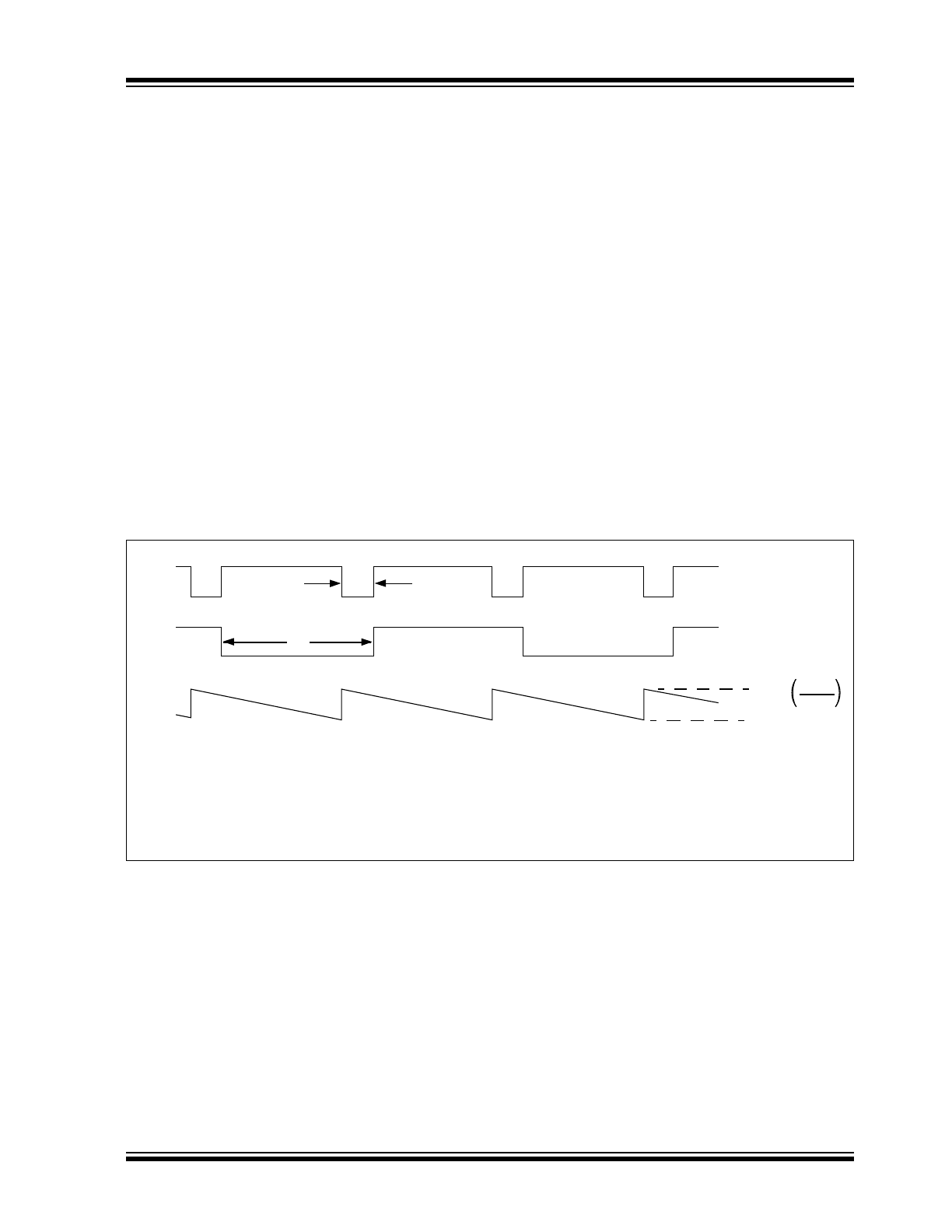
Threshold Detector Input
In the V/F mode, this input is connected to the AMPLI-
FIER OUT output (Pin 12) and triggers a 3 µs pulse
when the input voltage passes through its threshold. In
the F/V mode, the input frequency is applied to this
input.
The nominal threshold of the detector is half way
between the power supplies, or (V
DD
+ V
SS
)/2 ±400
mV. The TC9400’s charge balancing V/F technique is
not dependent on a precision comparator threshold,
because the threshold only sets the lower limit of the op
amp output. The op amp’s peak-to-peak output swing,
which determines the frequency, is only influenced by
external capacitors and by V
REF
.
2.10
Amplifier Out
This pin is the output stage of the operational amplifier.
During V/F operation, a negative going ramp signal is
available at this pin. In the F/V mode, a voltage
proportional to the frequency input is generated.
FIGURE 2-1:
Output Waveforms.
3 ms
Typ.
1/f
F
OUT
F
OUT
/2
Amp Out
VREF
0V
CREF
CINT
Note 1: To adjust F
MIN
, set V
IN
= 10 mV and adjust the 50 k
Ω offset for 10 Hz output.
2: To adjust F
MAX
, set V
IN
= 10V and adjust R
IN
or V
REF
for 10 kHz output.
3: To increase F
OUTMAX
to 100 kHz, change C
REF
to 2 pF and C
INT
to 75 pF.
4: For high performance applications, use high stability components for R
IN
, C
REF
. V
REF
(metal film
resistors and glass capacitors). Also, separate output ground (Pin 9) from input ground (Pin 6).
TC9400/9401/9402
DS21483D-page 8
© 2007 Microchip Technology Inc.
3.0
DETAILED DESCRIPTION
3.1
Voltage-to-Frequency (V/F) Circuit
Description
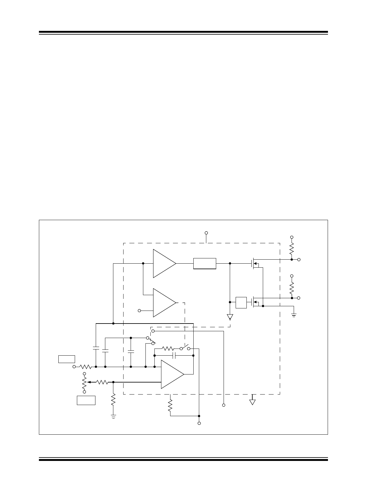
The TC9400 V/F converter operates on the principal of
charge balancing. The operation of the TC9400 is
easily understood by referring to
Figure 3-1
. The input
voltage (V
IN
) is converted to a current (I
IN
) by the input
resistor. This current is then converted to a charge on
the integrating capacitor and shows up as a linearly
decreasing voltage at the output of the op amp. The
lower limit of the output swing is set by the threshold
detector, which causes the reference voltage to be
applied to the reference capacitor for a time period long
enough to charge the capacitor to the reference volt-
age. This action reduces the charge on the integrating
capacitor by a fixed amount (q = C
REF
x V
REF
), causing
the op amp output to step up a finite amount.
At the end of the charging period, C
REF
is shorted out.
This dissipates the charge stored on the reference
capacitor, so that when the output again crosses zero,
the system is ready to recycle. In this manner, the con-
tinued discharging of the integrating capacitor by the
input is balanced out by fixed charges from the refer-
ence voltage. As the input voltage is increased, the
number of reference pulses required to maintain
balance increases, which causes the output frequency
to also increase. Since each charge increment is fixed,
the increase in frequency with voltage is linear. In
addition, the accuracy of the output pulse width does
not directly affect the linearity of the V/F. The pulse
must simply be long enough for full charge transfer to
take place.
The TC9400 contains a “self-start” circuit to ensure the
V/F converter always operates properly when power is
first applied. In the event that, during power-on, the op
amp output is below the threshold and C
REF
is already
charged, a positive voltage step will not occur. The op
amp output will continue to decrease until it crosses the
-3.0V threshold of the “self-start” comparator. When
this happens, an internal resistor is connected to the op
amp input, which forces the output to go positive until
the TC9400 is in its normal Operating mode.
The TC9400 utilizes low-power CMOS processing for
low input bias and offset currents, with very low power
dissipation. The open drain N-channel output FETs
provide high voltage and high current sink capability.
FIGURE 3-1:
10 Hz to 10 kHz V/F Converter.
–
+
+5V
+5V
14
V
DD
+5V
RL
10 k
Ω
RL
10 k
Ω
8
10
9
F
OUT
F
OUT
/2
11
3 ms
Delay
Self-
Start
12
5
20 k
Ω
60 pF
Op Amp
C
INT
820 pF
C
REF
180 pF
12 pF
R
IN
1 M
Ω
V
IN
+5V
-5V
50 k
Ω
510 k
Ω
10 k
Ω
3
1
Offset
Adjust
IIN
Zero Adjust
0V –10V
I
BIAS
V
SS
4
-5V
2
Output
Common
V
REF
OUT
R
BIAS
100 k
Ω
AMP OUT
TC9400
TC9401
TC9402
GND
6
Threshold
Detector
Threshold
Detect
Reference Voltage
(Typically -5V)
÷
2
V
REF
7
-3V
INPUT

© 2007 Microchip Technology Inc.
DS21483D-page 9
TC9400/9401/9402
3.2
Voltage-to-Time Measurements
The TC9400 output can be measured in the time
domain as well as the frequency domain. Some micro-
computers, for example, have extensive timing capabil-
ity, but limited counter capability. Also, the response
time of a time domain measurement is only the period
between two output pulses, while the frequency
measurement must accumulate pulses during the
entire counter time-base period.
Time measurements can be made from either the
TC9400’s PULSE FREQ OUT output, or from the
FREQ/2 OUT output. The FREQ/2 OUT output
changes state on the rising edge of PULSE FREQ
OUT, so FREQ/2 OUT is a symmetrical square wave at
one-half the pulse output frequency. Timing measure-
ments can, therefore, be made between successive
PULSE FREQ OUT pulses, or while FREQ/2 OUT is
high (or low).
TC9400/9401/9402
DS21483D-page 10
© 2007 Microchip Technology Inc.
4.0
VOLTAGE-TO-FREQUENCY
(V/F) CONVERTER DESIGN
INFORMATION
4.1
Input/Output Relationships
The output frequency (F
OUT
) is related to the analog
input voltage (V
IN
) by the transfer equation:
EQUATION 4-1:
4.2
External Component Selection
4.2.1
R
IN
The value of this component is chosen to give a full
scale input current of approximately 10 µA:
EQUATION 4-2:
EQUATION 4-3:
Note that the value is an approximation and the exact
relationship is defined by the transfer equation. In
practice, the value of R
IN
typically would be trimmed to
obtain full scale frequency at V
IN
full scale (see
Section 4.3 “Adjustment Procedure”, Adjustment
Procedure). Metal film resistors with 1% tolerance or
better are recommended for high accuracy applications
because of their thermal stability and low noise
generation.
4.2.2
C
INT
The exact value is not critical but is related to C
REF
by
the relationship:
3C
REF
≤
C
INT
≤
10C
REF
Improved stability and linearity are obtained when
C
INT
≤ 4C
REF
. Low leakage types are recommended,
although mica and ceramic devices can be used in
applications where their temperature limits are not
exceeded. Locate as close as possible to Pins 12
and 13.
4.2.3
C
REF
The exact value is not critical and may be used to trim
the full scale frequency (see Section 6.1 “Input/Out-
put Relationships”, Input/Output Relationships).
Glass film or air trimmer capacitors are recommended
because of their stability and low leakage. Locate as
close as possible to Pins 5 and 3 (see
Figure 4-1
).
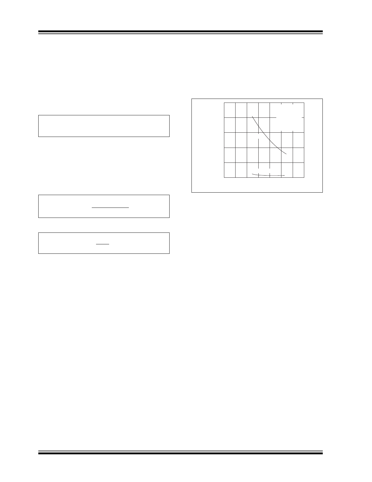
FIGURE 4-1:
Recommended C
REF
vs.
V
REF
.
4.2.4
V
DD
, V
SS
Power supplies of ±5V are recommended. For high
accuracy requirements, 0.05% line and load regulation
and 0.1 µF disc decoupling capacitors, located near the
pins, are recommended.
4.3
Adjustment Procedure
Figure 3-1
shows a circuit for trimming the zero
location. Full scale may be trimmed by adjusting R
IN
,
V
REF
, or C
REF
. Recommended procedure for a 10 kHz
full scale frequency is as follows:
1.
Set V
IN
to 10 mV and trim the zero adjust circuit
to obtain a 10 Hz output frequency.
2.
Set V
IN
to 10V and trim either R
IN
, V
REF
, or C
REF
to obtain a 10 kHz output frequency.
If adjustments are performed in this order, there should
be no interaction and they should not have to be
repeated.
4.4
Improved Single Supply V/F
Converter Operation
A TC9400, which operates from a single 12 to 15V
variable power source, is shown in
Figure 4-2
. This
circuit uses two Zener diodes to set stable biasing
levels for the TC9400. The Zener diodes also provide
the reference voltage, so the output impedance and
temperature coefficient of the Zeners will directly affect
power supply rejection and temperature performance.
Full scale adjustment is accomplished by trimming the
input current.
Frequency Out
V
IN
R
IN
--------
1
V
REF
(
) C
REF
(
)
------------------------------------
•
=
V
IN
FULL SCALE
10
μ
A
R
IN
≅
10V
10
μ
A
R
IN
≅
= 1 M
Ω
500
400
300
200
100
0
-1
-2
-3
-4
-5
-6
-7
V
REF
(V)
C
REF
(pF) +12pF
10 kHz
100 kHz
V
DD
= +5V
V
SS
= -5V
R
IN
= 1MW
V
IN
= +10V
T
A
= +25°C