
©
2005 Microchip Technology Inc.
DS21475C-page 1
TC818A
Features
• Auto-Ranging Analog-to-Digital Converter with
3-1/2 Digit Display
• Annunciator Outputs Permit Customizing of LCD
• Auto-Range Operation for AC and DC Voltage
and Resistance Measurements
• Two User Selected AC/DC
• Current Ranges: 20mA and 200mA
• 22 Operating Ranges: 9 DC/AC Voltage
• 4 AC/DC Current
• 9 Resistance and Low Power Ohms
• Display Hold Function
• 3-1/2 Digit Resolution in Auto-Range
Mode: 1/2000
• Extended Resolution in Manual Range
Mode: 1/3000
• Internal AC-to-DC Conversion Op Amp
• Triplex LCD Drive for Decimal Points, Digits,
• Bar Graphs, and Annunciators
• Continuity Detection and Piezoelectric
Transducer Driver
• Low Drift Internal Reference: 75ppm/°C
• 9V Battery Operation: 10mW
• Low Battery Detection and LCD Annunciator
Device Selection Table
General Description
The TC818A is an integrating analog-to-digital con-
verter (ADC) with a 3-1/2 digit numeric LCD driver,
automatic ranging, and single 9V battery operation.
The numeric display provides 0.05% resolution and a
full set of annunciators that spell out the TC818A's
many operating modes.
Automatic range selection is provided for both voltage
(DC and AC) and ohms (high and low power) measure-
ments. Expensive and bulky mechanical range
switches are not required. Five full scale ranges are
available, with automatic selection of external volt/ohm
attenuators over a 1 to 10,000 range. Two current
ranges, 20mA and 200mA, can be manually selected.
The auto-range feature can be bypassed, allowing
input attenuator selection through a single line input.
During Manual mode operation, resolution is extended
to 3000 counts full scale. Extended resolution is also
available during 2000k
Ω
and 2000V full scale auto-
range operation. The extended range operation is indi-
cated by a flashing 1 MSD and by the fully extended bar
graph.
The TC818A includes an AC-to-DC converter for AC
voltage and current measurements. Only external
diodes/resistors/capacitors are required. Other fea-
tures include a Memory mode, low battery detection,
display HOLD input, and continuity buzzer driver.
The 3-1/2 digit numeric display includes a full set of
annunciators. Decimal points are adjusted as auto-
matic or manual range changes occur, and Voltage,
Current, and Ohms Operating modes are displayed.
Additional annunciators are activated for manual, auto,
memory, HOLD, AC, low power ohms, and low battery
conditions.
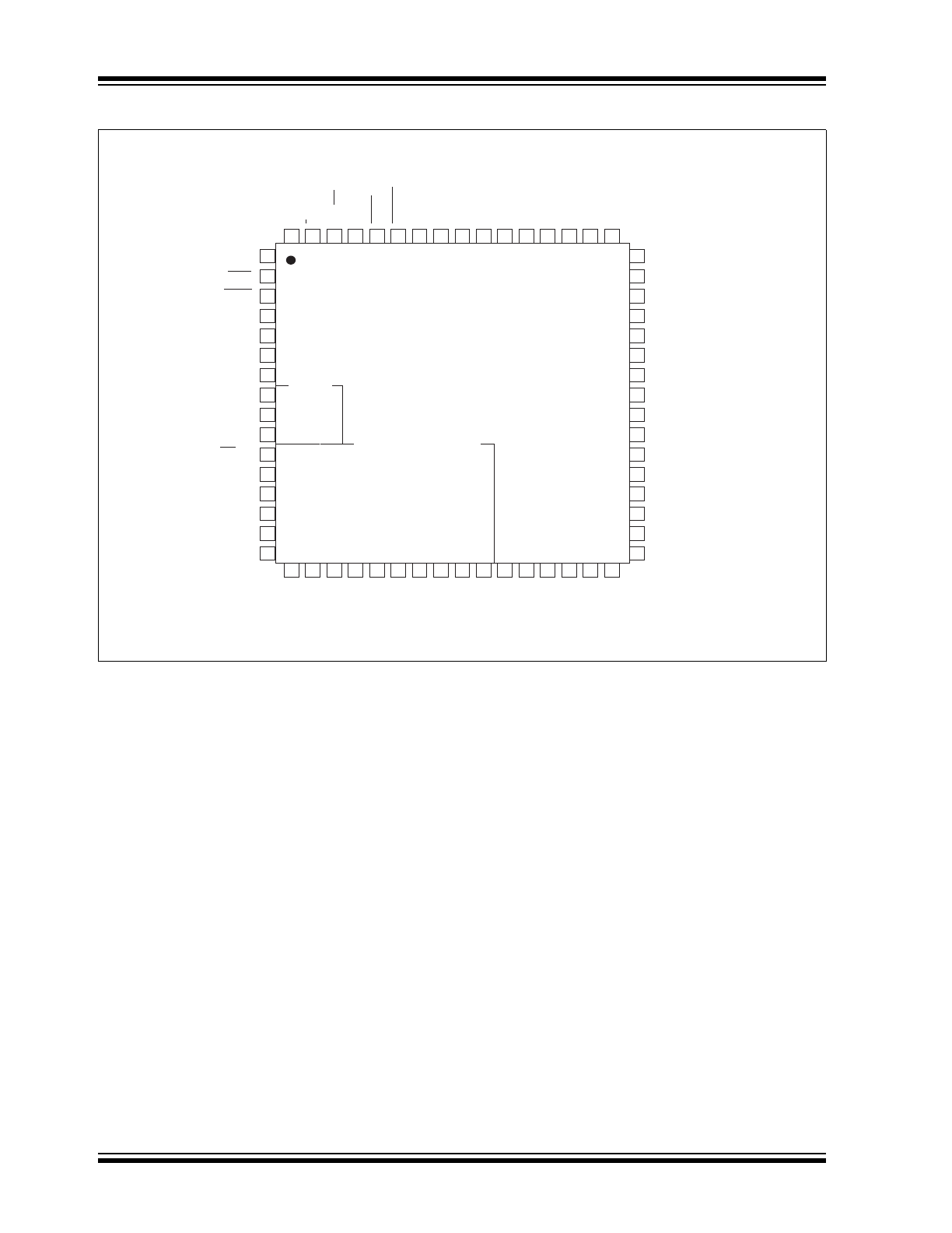
The TC818A is available in a surface mounted 64-pin
flat package. Combining a numeric display driver, sin-
gle 9V battery operation, internal range switching, and
compact surface mounting, the TC818A is ideal for
advanced portable instruments.
Part Number
Package
Operating
Temperature Range
TC818ACBU
64-Pin PQFP
0
°
C to +70
°
C
Auto-Ranging Analog-to-Digital Converter
with 3-1/2 Digit Display
Obsolete Device
TC818A
DS21475C-page 2
©
2005 Microchip Technology Inc.
Package Type
47
52
51
50
49
64
63
62
58
57
56
55
54
53
60
59
24
25
26
27
28
29
30
18
19
20
21
22
23
32
17
1
2
3
4
5
6
7
8
9
10
11
12
13
14
15
45
44
43
42
41
40
39
38
37
36
35
34
33
48
TC818A
R
X
CFI
ADI
ADO
R
Ω
BUF
RVIBUF
ACVH
DGND
RANGE
-MEM
I
HOLD
C
REFL
RM
REFL
DEINT
COM
V
CC
AC/-/AUTO
BCP3
ANNUNC
FE2
AGD2
-MEM/BATT
BCP2
FE1
AGD1
BCP1
C
I
ACVL
I
I
C
REFH
REFHI
ΩR3
V
I
VR4
VR5
VR2
VR3
ΩR5
ΩR4
ΩR2
ΩR1
DC(
Ω
)/
AC(LO
Ω
)
V
SS
C
AZ
LCD
Backplanes
LCD Segment Drives
16
OHM
20mA
BUZ
FE0
AGD0
BCP0
XTAL1
XTAL2
V
DISP
BP1
BP2
BP3
LO
Ω/A
Ω/V
k/m/
HOLD
NC
46
NC
61
NC
31
NC
64-Pin PQFP
©
2005 Microchip Technology Inc.
DS21475C-page 3
TC818A
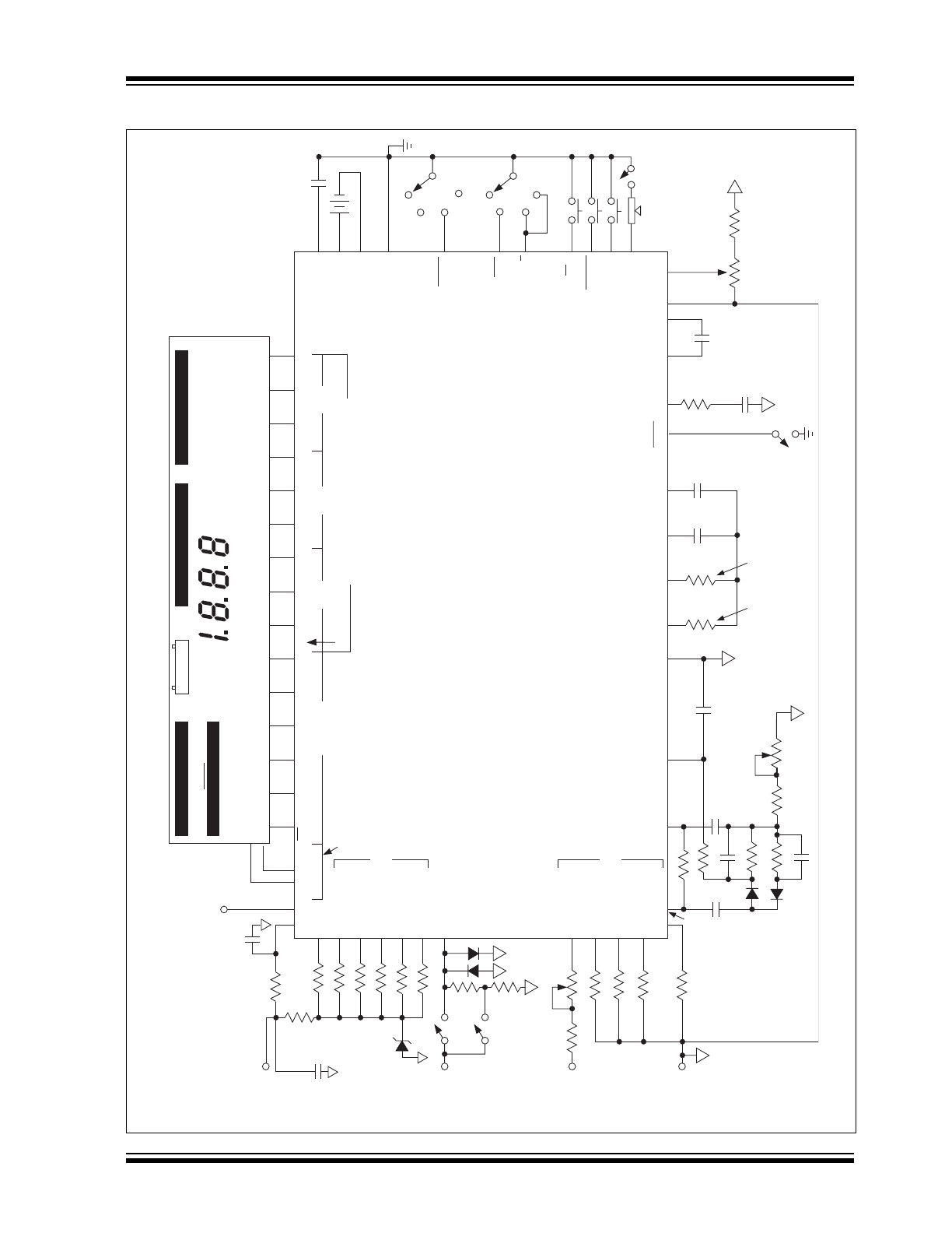
Typical Application
–
50
TC818A
0.1µF
LCD Bias
R7/100k
Ω
R6/100k
Ω
Z1
6.2V
31
39
1.6385M
Ω
0.1
µF
R8/220
Ω
(PTC)
38
37
36
35
Ω
R5 (÷10,000)
Ω
R4 (÷1,000)
Ω
R3 (÷100)
Ω
R2 (÷10)
Ω
R1 (÷1)
RM
REFL
R
X
78
9
10
27
163.85k
Ω
R2/1638.5
Ω
R1/163.85
Ω
R3/16.385k
Ω
Ohms Range Attenuator
V
DISP
BP3
ANNUNC
LO
Ω
/A
Ω
/V
k/m/
HOLD
–MEM/
BATT
FE2
FE1
BCP2
AGD1
BCP1
FE0
AGD0
BCP0
XTAL1
DEINT
5
30
6
28
57
14
15
16
18
19
20
21
22
23
24
26
25
13
12
11
-MEM
LO
–+
AC
mVA
32.768kHz
(~ 33kHz)
39pF
9V
58
XTAL2
V
SS
45
DGND
V
62
59
61
RANGE
-MEM
BUZ
4
Enable
Audio
Transducer
Current
Input
20mA
200mA
R15
D3
D4
R16
I
I
Voltage
Input
R14/9.9M
Ω
44
R13*
500k
Ω
R12/1.111M
Ω
R11/101k
Ω
41
R10/10k
Ω
VR1
Voltage Range Attenuator
(÷1)
VR2
(÷10)
VR3
(÷100)
VR4
(÷1,000)
VR5
(÷10,000)
ADO
R9/1k
Ω
40
43
34
53
D1
29
REFHI
COM
33
C
REF
32
C
F
I
51
R20
100k
Ω
C6
0.01µF
60
HOLD
C
I
47
R26/3k
Ω
R27/2k
Ω
–+
C5/1µF
R24/10k
Ω
R23/10k
Ω
ADI
R21/2.2M
Ω
52
+
R22/470k
Ω
C4/1µF
4.7µF
C2/0.22µF
ACVH
56
C1/1µF
ACVL
46
R
Ω
BUF
RVIBUF
49
RVIBUF
55
R
Ω
BUF
C
AZ
0.1µF
150
k
220
k
SYNC
Backplane
Drivers
1000's
Segment and Decimal Point Drive
1Ω
9Ω
W
163.85mV
Positive
Temperature
Coefficient
Resistor
AUTO
HOLD
R19/5k
Ω
V
CC
*Not required when Resistor Network is used.
(See Applications Section for details.)
D2
AGD2
C
AZ
V
CC
42
C
INT
C
REFL
C
REFH
DC/AC or
Ω
/LO
Ω
kΩ
BP1
BP2
BCP3
AC/–/
AUTO
100's
10's
1's
Display
Annunciators
COM
ΩΩ
R18/24k
Ω
Resistance
Input
54
HOLD
200mA
20mA
200mA
OHM
3
2
63
200mA
20mA
I
Ω
V
Ω
TC818A
DS21475C-page 4
©
2005 Microchip Technology Inc.
1.0
ELECTRICAL
CHARACTERISTICS
Absolute Maximum Ratings*
Supply Voltage .......................................................15V
Analog Input Voltage ..................................V
CC
to V
SS
Reference Input Voltage..............................V
CC
to V
SS
Voltage at Pin 43 ................................. Common ±0.7V
Power Dissipation ............................................800mW
Operating Temperature Range................ 0°C to +70°C
Storage Temperature Range ..............-65°C to +150°C
*Stresses above those listed under "Absolute Maximum
Ratings" may cause permanent damage to the device. These
are stress ratings only and functional operation of the device
at these or any other conditions above those indicated in the
operation sections of the specifications is not implied.
Exposure to Absolute Maximum Rating conditions for
extended periods may affect device reliability.
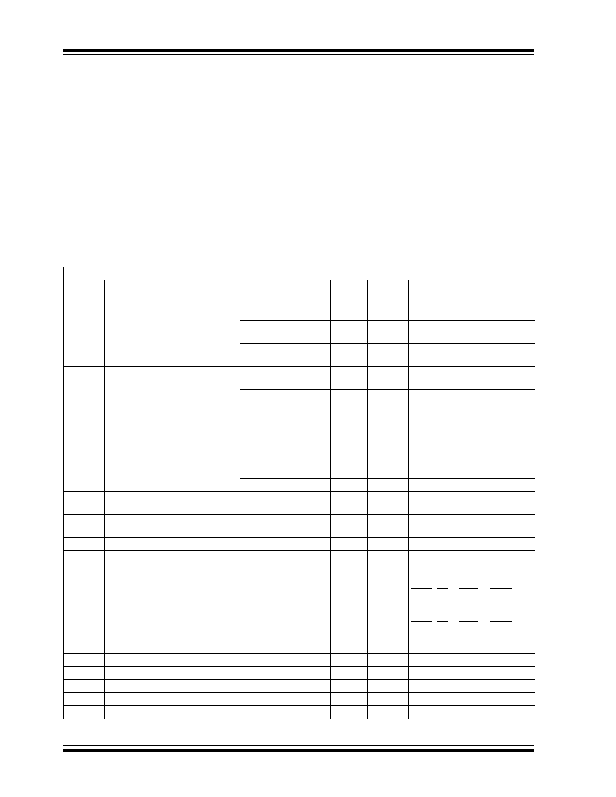
TC818A ELECTRICAL SPECIFICATIONS
Electrical Characteristics: V
A
= 9V, T
A
= +25°C, unless otherwise specified.
Symbol
Parameter
Min
Typ
Max
Unit
Test Conditions
Zero Input Reading
-0000
0000
+0000
Digital
Reading
200mV Range without 10M
Ω
Resistor
-0001
—
+0001
Digital
Reading
200mV Range with 10M
Ω
Resistor
-0000
0000
+0000
Digital
Reading
20mA and 200mA Range
RE
Rollover Error
—
—
±1
Counts
200mV Range without 10M
Ω
Resistor
—
—
±3
200mV Range with 10M
Ω
Resistor
—
—
±1
20mA and 200mA Range
NL
Linearity Error
—
—
±1
Count
Best Case Straight Line
I
IN
Input Leakage Current
—
—
10
pA
E
N
Input Noise
—
20
—
μ
V
P-P
BW = 0.1 to 10Hz
AC Frequency Error
—
±1
—
%
40 to 500Hz
—
±5
—
%
Error 40 to 2000Hz
Open Circuit Voltage for Ohm
Measurements
—
570
660
mV
Excludes 200
Ω
Range
Open Circuit Voltage for LO Ohm
Measurements
—
285
350
mV
Excludes 200
Ω
Range
V
COM
Analog Common Voltage
2.8
3
3.3
V
(V
CC
- V
COM
)
V
CTC
Common Voltage Temperature
Coefficient
—
—
50
ppm/°C
Display Multiplex Rate
—
100
—
Hz
V
IL
Low Logic Input
—
—
1
μ
A
20mA, AC, I, LOW
Ω
, HOLD
Range, -MEM, OHMs
(Relative to DGND, Pin 58)
Logic 1 Pull-up Current
—
25
—
V
20mA, AC, I, LOW
Ω
, HOLD
Range, -MEM, OHMs
(Relative to DGND, Pin 58)
V
OL
Low Logic Output
—
DGND +0.1
—
V
ANNUNC, DEINT: I
L
= 100
μ
A
V
OH
High Logic Output
—
V
CC
- 0.1
—
V
ANNUNC, DEINT: I
L
= 100
μ
A
Buzzer Drive Frequency
—
4
—
kHz
Low Battery Flag Voltage
6.3
6.6
7
V
V
CC
to V
SSA
Operating Supply Current
—
0.8
1.5
mA
©
2005 Microchip Technology Inc.
DS21475C-page 5
TC818A
2.0
PIN DESCRIPTIONS
The descriptions of the pins are listed in Table 2-1.
TABLE 2-1:
PIN FUNCTION TABLE
Pin Number
(64-Pin PQFP)
Symbol
Description
1
NC
No connection.
2
OHM
Logic Input. “0” (Digital Ground) for resistance measurement.
3
20mA
Logic Input. “0” (Digital Ground) for 20mA full scale current measurement.
4
BUZ
Buzzer. Audio frequency, 4kHz, output for continuity indication during resistance
measurement. A noncontinuous 4kHz signal is output to indicate an input over range
during voltage or current measurements.
5
XTAL1
32.768kHz Crystal Connection.
6
XTAL2
32.768kHz Crystal Connection.
7
V
DISP
Sets peak LCD drive signal: V
P
- V
DD
-V
DISP
. V
DISP
may also be used to compensate for
temperature variation of LCD crystal threshold voltage.
8
BP1
LCD Backplane #1.
9
BP2
LCD Backplane #2.
10
BP3
LCD Backplane #3.
11
LO
Ω
/A
LCD Annunciator segment drive for low ohms resistance measurement and current
measurement.
12
Ω
/V
LCD Annunciator segment drive for resistance measurement and voltage measurement.
13
k/m/HOLD
LCD Annunciator segment drive for k (“kilo-Ohms”), m (“milliamps” and “millivolts”) and
HOLD mode.
14
BCP0
(One’s digit)
LCD segment drive for “b,” “c” segments and decimal point of least significant digit (LSD).
15
AGD0
LCD segment drive for “a,” “g,” “d” segments of LSD.
16
FE0
LCD segment drive for “f” and “e” segments of LSD.
17
NC
No connection.
18
BCP1
LCD segment drive for “b,” “c” segments and decimal point of 2nd LSD.
19
AGD1
LCD segment drive for “a,” “g,” “d” segments of 2nd LSD.
20
FE1
LCD segment drive for “f” and “e” segments of 2nd LSD.
21
BCP2
LCD segment drive for “b,” “c” segments and decimal point of 3rd LSD
(hundred’s digit).
22
AGD2
LCD segment drive for “a,” “g,” “d” segments of 3rd LSD.
23
FE2
LCD segment drive for “f,” “e” segments of 3rd LSD.
24
BCP3
LCD segment drive for “b,” “c” segments and decimal point of MSD,
(thousand’s digit).
25
AC/-/AUTO
LCD annunciator segment drive for AC measurements, polarity, and auto-range operation.
26
-MEM/BATT LCD annunciator segment drive for AC for low battery indication and memory (relative
measurement).
27
ANNUNC
Square wave output at the backplane frequency, synchronized to BP1. ANNUNC can be
used to control display annunciators. Connecting an LCD segment to ANNUNC turns it on;
connecting it to its backplane turns it off.
28
V
CC
Positive battery supply connection.
29
COM
Analog circuit ground reference point. Nominally 3V below V
CC
.
30
DEINT
De-integrate output.
31
RM
REFL
Ratiometric (resistance measurement) reference low voltage.
32
C
REFL
Reference capacitor negative terminal C
REF
= 0.1
μ
f.
33
C
REFH
Reference capacitor positive terminal C
REF
= 0.1
μ
f.
34
REFHI
Reference voltage for voltage and current measurement. Nominally 163.85mV.
35
Ω
R1
Standard resistor connection for 200
Ω
full scale.
36
Ω
R2
Standard resistor connection for 2000
Ω
full scale.
TC818A
DS21475C-page 6
©
2005 Microchip Technology Inc.
3.0
DETAILED DESCRIPTION
3.1
Analog-to-Digital Converter (ADC)
The TC818A includes an integrating ADC with auto-
ranging resolution of 2000 counts and manual range
resolution of 3000 counts. Figure 3-1 shows a simpli-
fied schematic of the analog section. In Auto-Ranging
mode, internal logic will adjust the input voltage or
ohms attenuators so that measurements will always be
made in the appropriate range.
Measurement ranges, logic control inputs, 3-1/2 digit
LCD formatting, and other features are identical to the
TC818A auto-ranging A/D converter. However, the
TC818A is not pin compatible with, and is not a replace-
ment for, the TC818A.
A display annunciator output (ANNUNC) can be used
to customize the LCD. ANNUNC is a square wave at
the backplane frequency. Connecting an annunciator
segment to the ANNUNC driver turns the segment on;
connecting the segment to its backplane turns it off.
37
Ω
R3
Standard resistor connection for 20k
Ω
full scale range.
38
Ω
R4
Standard resistor connection for 200k
Ω
full scale range.
39
Ω
R5
Standard resistor connection for 2000k
Ω
full scale.
40
VR3
Voltage measurement
÷
100 attenuator.
41
VR2
Voltage measurement ÷
10 attenuator.
42
VR5
Voltage measurement ÷ 10,000 attenuator.
43
VR4
Voltage measurement ÷ 1000 attenuator.
44
V
I
Unknown voltage input ÷ attenuator.
45
I
I
Unknown current input.
46
ACVL
Low output of AC-to-DC converter.
47
C
I
Integrator capacitor connection. Nominally 0.1
μ
F. (Must have low dielectric absorption.
Polypropylene dielectric suggested.)
48
NC
No connection.
49
C
AZ
Auto-zero capacitor connection. Nominally 0.1
μ
F.
50
R
X
Unknown resistance input.
51
CFI
Input filter connection.
52
ADI
Negative input of internal AC-to-DC operational amplifier.
53
ADO
Output of internal AC-to-DC operational amplifier.
54
R
Ω
BUF
Active buffer output for resistance measurement. Integration resistor connection.
Nominally 220k
Ω
.
55
RVIBUF
Active buffer output for voltage and current measurement. Integration resistor connection.
Nominally 15k
Ω
.
56
ACVH
Positive output of AC-to-DC converter.
57
V
SS
Negative supply connection. Connect to negative terminal of 9V battery.
58
DGND
Internal logic digital ground. Ground connection for the logic "0" level.
Nominally 4.7V below V
CC
.
59
RANGE
Input to set manual operation and change ranges.
60
HOLD
Input to hold display. Connect to DGND to "FREEZE" display.
61
-MEM
Input to enter Memory Measurement mode for relative measurements. The two LSDs are
stored and subtracted from future measurements.
62
DC(
Ω
)/
AC(LO
Ω
)
Input that selects AC or DC option during voltage/current measurements. For resistance
measurements, the ohms or low power (voltage) ohms option can be selected.
63
I
Input to select measurement. Connect to logic "0" (digital ground) for current measurement.
64
NC
No connection.
TABLE 2-1:
PIN FUNCTION TABLE (CONTINUED)
Pin Number
(64-Pin PQFP)
Symbol
Description
©
2005 Microchip Technology Inc.
DS21475C-page 7
TC818A
FIGURE 3-1:
TC818A ANALOG SECTION
TC818A
+
–
2.8VREF AMP
10k
V
CC
1.5
Ω
S43
V
CC
R18/24k
V
CC
R19/5k
Analog
Cmmon
29
REFHI
163.85mV
≈
0.1µF
C
REFH
51 CFI
0.01µF
C6
R20/100k
Ω
To Digital
Section
S38 AZ
Comparator
Integrator
49
47
INT
0.01µF
0.01µF
C
INT
55
RVI
BUF
150
k
54
R
BUF
220
k
R
ΩBUF
R
ΩBUF
S34
DE •
S20 DE
S18 DE
S19 DE+
S16 DE+
S17 DE-
Buffer
S35
S37
INT+
Ω + DC
C1/1µF
0.22µF
ACVH
S15 AZ
39
38
37
36
35
31
50
R
X
R7/100 k
Ω
R6/100k
Ω
R5/1.638M
Ω
R1/163.85
Ω
R4/163.85k
Ω
R3/16385
Ω
R2/1638.5
Ω
RM
REFL
R5
ΩR4
ΩR3
ΩR2
ΩR1
0.1µF
Ohms
Input
Current Input
R8/220
0.1µF
(PTC)
D3
6.2V
200mA
D4
R15/9
Ω
20mA
R16/1
I 45
I
R12/1.11M
R11/101k
R10/10k
R9/1k
ACVH 46
R24
10k
R23
10k
Ω
R26
3k
Ω
R27/2k
Ω
Common
D2
C3
1µF
C4
1µF
V 44
I
VR2 41
VR3 40
VR4 43
VR5 42
ADO
ADI
Voltage
Input
R22
470
k
Ω
R21
2.2
M
R14/9.9 M
Ω
R13/500k
Ω*
4.7µF
Z1
S28
S27
S26
S25
S21 DE •
S12 V • 1/1
1/1k
•
1/100
•
1/10
•
1/1
•
+AC
INT•(
Ω + DC)
S11
S13
AC-to-DC
Converter
Op Amp
V•1/1
V•1/10
V•1/100
V•1/1k
V•1/10k
1/10 1/1001/1k 1/10k
S32
S33
S31 S30 S29
1/1
•
V
CC
S10
W + 1
S6
S7
S8 S9
S1
S2
S3
S4
S5
*Not Required when Resistor
Network is Used
INT•
Ω •ACΩ
V•
1/10
V•
1/100
V•
1/1
k
V•
1/10k
D1
DE
33 C
REFH
32 C
REFL
C
AZ
+
+
53
S24
Ω 1/10k
•
•
•
•
•
C
AZ
S44
HI
•
•
S14
S40
INT•
Ω•ACΩ
LO
Ω
•
52
56
S22
S22
C2
S39
1.5 k
Ω
Ω
Ω
Ω
Ω
Ω
Ω
Ω
Ω
Ω
Ω
Ω
Ω
Ω
Ω
Ω
Ω
Ω
Ω
Ω
Ω
Ω Ω
Ω
Ω
Ω
Ω
Ω
Ω
Ω
Ω
Ω
Ω
Ω
Ω
Ω
Ω
Ω
+
–
+
–
+
–
+
–
+
–
34
TC818A
DS21475C-page 8
©
2005 Microchip Technology Inc.
3.2
Resistance, Voltage, Current
Measurement Selection
The TC818A is designed to measure voltage, current,
and resistance. Auto-ranging is available for resistance
and voltage measurements. The OHM (Pin 2) and
I (Pin 63) input controls are normally pulled internally to
V
CC
.
By tying these pins to DGND (Pin 58), the TC818A is
configured internally to measure resistance, voltage, or
current. The required signal combinations are shown in
Table 3-1.
TABLE 3-1:
TC818A MEASUREMENT
SELECTION LOGIC
Note
1:
OHM and I are normally pulled internally high to
V
CC
(Pin 28). This is considered a logic “1”.
2: Logic “0” is the potential at digital ground (Pin 58).
3.3
Resistance Measurements
(Ohms and Low Power Ohms)
The TC818A can be configured to reliably measure in-
circuit resistances shunted by semiconductor junc-
tions. The TC818A Low Power Ohms Measurement
mode limits the probe open circuit voltage. This pre-
vents semiconductor junctions in the measured system
from turning on.
In the Resistance Measurement mode, the
Ω
/LO
Ω
(Pin 62) input selects the Low Power Ohms Measure-
ment mode. For low power ohms measurements,
Ω
/LO
Ω
(Pin 62) is momentarily brought LOW to digital
ground potential. The TC818A sets up for a low power
ohms measurement, with a maximum open circuit
probe voltage of 0.35V above analog common. In the
Low Power Ohms mode, an LCD display annunciator,
LO
Ω
, will be activated. On power-up, the Low Power
Ohms mode is not active.
If the Manual Operating mode has been selected, tog-
gling
Ω
/LO
Ω
resets the TC818A back to the Auto-
Range mode. In Manual mode, the decision to make a
normal or low power ohms measurement should be
made before selecting the desired range.
The low power ohms measurement is not available on
the 200
Ω
full scale range. Open circuit voltage on this
range is below 2.8V. The standard resistance values
are listed in Table 3-2.
R8, a positive temperature coefficient resistor, and the
6.2V zener, Z1, provide input voltage protection during
ohms measurements.
TABLE 3-2:
OHMS RANGE LADDER
NETWORK
3.4
Ratiometric Resistance
Measurements
The TC818A measures resistance ratiometrically.
Accuracy is set by the external standard resistors con-
nected to Pin 35 through 39. A Low Power Ohms mode
may be selected on all but the 200
Ω
full scale range.
The Low Power Ohms mode limits the voltage applied
to the measured system. This allows accurate “in-
circuit” measurements when a resistor is shunted by
semiconductor junctions.
Full auto-ranging is provided. External precision stan-
dard resistors are automatically switched to provide the
proper range.
Figure 3-2 shows a detailed block diagram of the
TC818A, configured for ratiometric resistance measure-
ments. During the signal integrate phase, the reference
capacitor charges to a voltage inversely proportional to
the measured resistance, R
X
. Figure 3-3 shows that the
conversion accuracy relies on the accuracy of the
external standard resistors.
Normally, the required accuracy of the standard resis-
tances will be dictated by the accuracy specifications of
the users end product. Table 3-3 gives the equivalent
ohms per count for various full scale ranges to allow
users to judge the required resistor for accuracy.
TABLE 3-3:
REFERENCE RESISTORS
Function Select Pin
0 = Digital Ground
1 = Floating or Tied to V
CC
Selected
Measurement
OHM (Pin 2)
I (Pin 63)
0
0
Voltage
0
1
Resistance
1
0
Current
1
1
Voltage
Full-Scale
Range
Standard
Resistance
Low Power
Ohms Mode
200
Ω
163.85
Ω
(R1)
NO
2000
Ω
1638.5k
Ω
(R2)
YES
20k
Ω
16,385
Ω
(R3)
YES
200k
Ω
163,85
Ω
(R4)
YES
2,000k
Ω
1,638,500
Ω
(R5)
YES
Full Scale
Range
Reference Resistor
Ω
/Count
200k
163.85
0.1
2k
1638.5
1
20k
16385
10
200k
163,850
100
2M
1,638,500
1000
©
2005 Microchip Technology Inc.
DS21475C-page 9
TC818A
FIGURE 3-2:
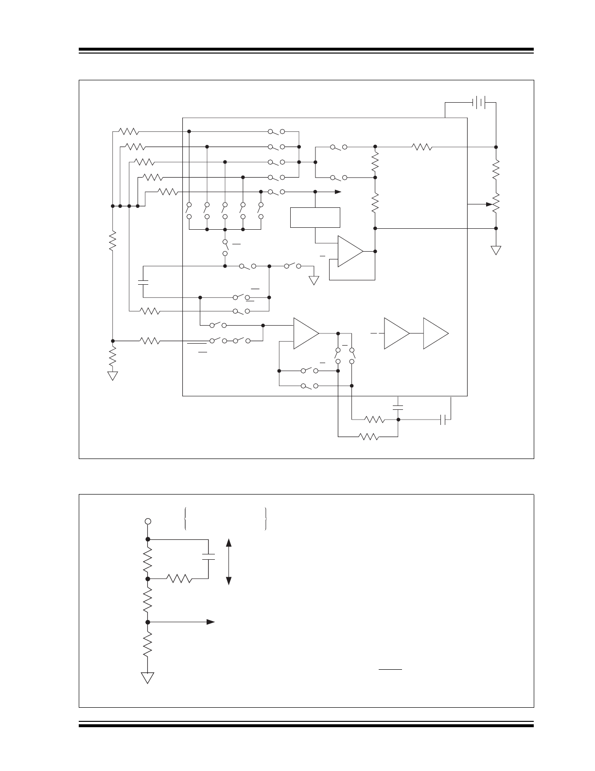
RATIOMETRIC RESISTANCE MEASUREMENT FUNCTIONAL DIAGRAM
FIGURE 3-3:
RESISTANCE MEASUREMENT ACCURACY SET BY EXTERNAL
STANDARD RESISTOR
Buffer
TC818A
R6/100k
Ω
32
S19
DE
S20
V
CC
-2.6V
1.5k
Ω
V
CC
Low Ohms
HI
Ohms
VA
S29
S30
S31
S32
S33
÷1
÷10
÷100
÷1k
÷10k
S28
S27
S26
S25
S24
DE
S23
Voltage
Reference
39
38
37
36
35
÷1
÷10
÷100
÷1k
÷10k
Integrator
Comparator
S37
S35
55
54
R
ΩBUF
S12
S13
DE
S18
S21
DE
INT • ( + DC)
33
C
REF
0.1µF
R7/100k
Ω
31
Analog
Common
29
34
28
10k
57
V
SS
9V
R18
24k
Ω
5k
Ω
REFHI
220k
49
0.1µF
150k
Ω
RVIBUF
47
C
INT
0.1µF
S36
S34
R
X
Unknown
R8
220
Ω
(PTC)
V •
1
1
R5/1638500
R4/163850
R3/16385
R2/1638.5
R1/163.85
Ω
Ω
DE +
Ω
• LO
C
AZ
≈ V
CC
-2.8V
V
CC
+
~
1.5k
Ω
~
•
•
•
DE
•
•
•
50
Ω
Ω
Ω
Ω
Ω
Ω
Ω
Ω
Ω
Ω
Ω
Ω
Ω
Ω
Ω
+
–
Example: 200k
Ω
Full Scale Measurement
V
R
163.85k
Ω
163.85
220
R
X
+
+
-------------------------------------------------
⎝
⎠
⎛
⎞
x0.64
=
(a )
(b)
V
X
R
X
163.85k
Ω
220
Ω
R
X
+
+
--------------------------------------------------------------
⎝
⎠
⎛
⎞
x0.64
=
(c) “Ramp Up Voltage” = “Ramp Down Voltage”
V
X
R
I
C
I
(
)
----------------xT
I
V
X
R
I
C
I
(
)
----------------T
DE
=
.
. .
Where:
R
I
= Integrating Resistor, T
I
= Integrate Time
C
I
= Integrating Capacitor, T
DE =
De-integrate Time
(d)
R
X
= 163.85
T
I
(T
DE
)
Independent of R
I
, C
I
or Internal Voltage Reference
163.85k
Ω
C
REF
220
R
X
Unknown
To Analog Buffer
100k
Ω
VA = 0.64V for Ohms
0.32V for LO Ohms
+
Ω
R
S
V
R
V
X

TC818A
DS21475C-page 10
©
2005 Microchip Technology Inc.
3.5
Voltage Measurement
Resistive dividers are automatically changed to provide
in range readings for 200mV to 2000V full scale read-
ings (Figure 3-1). The input resistance is set by exter-
nal resistors R14/R13. The divider leg resistors are R9-
R12. The divider leg resistors give a 200mV signal V
I
(Pin 44) for full scale voltages from 200mV to 2000V.
For applications which do not require a 10m
Ω
input
impedance, the divider network impedances may be
lowered. This will reduce voltage offset errors induced
by switch leakage currents.
3.6
Current Measurement
The TC818A measures current only under manual
range operation. The two user selectable, full scale
ranges are: 20mA and 200mA. Select the current Mea-
surement mode by holding the I input (Pin 63) LOW at
digital ground potential. The OHM input (Pin 2) is left
floating or tied to the positive supply.
Two ranges are possible. The 20mA full scale range is
selected by connecting the 20mA input (Pin 3) to digital
ground. If left floating, the 200mA full scale range is
selected.
External current-to-voltage conversion resistors are
used at the current input (I
I
input, Pin 45). For 20mA
measurements, a 10
Ω
resistor is used. The 200mA
range requires a 1
Ω
resistor; full scale is 200mV.
Printed circuit board trace resistance between analog
common and R16 must be minimized. In the 200mA
range, for example, a 0.05 trace resistance will cause a
5% current-to-voltage conversion error at I
I
(Pin 45).
The extended resolution measurement option operates
during current measurements.
To minimize rollover error, the potential difference
between analog common (COM, Pin 29) and system
common must be minimized.
3.7
AC-to-DC Measurements
In voltage and current measurements, the TC818A can
be configured for AC measurements. An on-chip oper-
ational amplifier and external rectifier components per-
form the AC-to-DC conversion.
When power is first applied, the TC818A enters the DC
Measurement mode. For AC measurements (current or
voltage), AC/DC (Pin 62) is momentarily brought LOW
to digital ground potential; the TC818A sets up for AC
measurements, and the AC liquid crystal display
annunciator activates. Toggling AC/DC LOW again
returns the TC818A to DC operation.
If the Manual Operating mode has been selected, tog-
gling AC/DC resets the TC818A back to the Auto-
Range mode. In Manual mode operation, AC or DC
should be selected first, then the desired range.
The minimum AC full scale voltage range is 2V. The DC
full scale minimum voltage is 200mV.
AC current measurements are available on the 20mA
and 200mA full scale current ranges.
3.8
Conversion Timing
The TC818A analog-to-digital converter uses the con-
ventional dual slope integrating conversion technique,
with an added phase that automatically eliminates zero
offset errors. The TC818A gives a zero reading with a
0 volt input.
The TC818A is designed to operate with a low cost,
readily available 32.768kHz crystal. It serves as a time-
base oscillator crystal in many digital clocks. (See
External Crystal Sources.)
The external clock is divided by two. The internal clock
frequency is 16.348kHz, giving a clock period of
61.04µsec. The total conversion — auto-zero phase,
signal integrate and reference de-integrate — requires
8000 clock periods or 488.3msec. There are approxi-
mately two complete conversions per second.
The integration time is fixed at 1638.5 clock periods or
100msec. This gives rejection of 50/60Hz AC line
noise.
The maximum reference de-integrate time, represent-
ing a full scale analog input, is 3000 clock periods
(183.1msec) during manual extended resolution oper-
ation. The 3000 counts are available in Manual mode,
extended resolution operation only. In Auto-Ranging
mode, the maximum de-integrate time is 2000 clock
periods. The 1000 clock periods are added to the auto-
zero phase. An auto-ranging or manual conversion
takes 8000 clock periods. After a zero crossing is
detected in the Reference De-integrate mode, the auto-
zero phase is entered. Figure 3-4 shows the basic
TC818A timing relationships.