
©
2005 Microchip Technology Inc.
DS21474C-page 1
TC815
Features
• Auto-Range Operation for AC and DC Voltage
and Resistance Measurements
- Two User Selected AC/DC Current Ranges
20mA and 200mA
• 22 Operating Ranges
- 9 DC/AC Voltage
- 4 AC/DC Current
- 9 Resistance and Low Power Ohms
• Display HOLD Function
• 3-1/2 Digit Resolution in Auto-Range Mode:
- 1/2000
• Extended Resolution in Manual Mode: 1/3000
• Memory Mode for Relative Measurements:
- ±5% F.S.
• Internal AC to DC Conversion Op Amp
• Triplex LCD Drive for Decimal Points, Digits
and Annunciators
• Continuity Detection and Piezoelectric
Transducer Driver
• Compact Surface Mounted 64-pin
Plastic Flat Package
• Low Drift Internal Reference: 75ppm/°C
• 9V Battery Operation: 10mW
• Low Battery Detection and LCD Annunciator
Device Selection Table
General Description
The TC815 is a 3-1/2 digit integrating analog-to-digital
converter with triplex LCD display drive and automatic
ranging. A display hold function is on-chip. Input volt-
age/ohm attenuators ranging from 1 to 1/10,000 are
automatically selected. Five full scale ranges are pro-
vided. The CMOS TC815 contains all the logic and
analog switches needed to manufacture an auto-
ranging instrument for ohms and voltage measure-
ments. User selected 20mA and 200mA current ranges
are available. Full scale range and decimal point LCD
annunciators are automatically set in auto-range oper-
ation. Auto-range operation is available during ohms
(high and low power ohms) and voltage (AC and DC)
measurements, eliminating expensive range switches
in hand-held DMM designs. The auto-range feature
may be bypassed allowing decimal point selection and
input attenuator selection control through a single line
input. Expensive rotary switches are not required.
During Manual mode operation, resolution is extended
to 3000 counts full scale. The extended range opera-
tion is indicated by a flashing 1 MSD. The extended
resolution is also available during 200k
Ω
and 2000V
full scale auto-range operation.
The Memory mode subtracts a reading, up to ±5% of
full scale from subsequent measurements. Typical
applications involve probe resistance compensation for
resistance measurements, tolerance measurements,
and tare weight measurements.
The TC815 includes an AC to DC converter for
AC measurements. Only external diodes/resistors/
capacitors are required.
A complete LCD annunciator set describes the TC815
meter function and measurement range during ohms,
voltage and current operation. AC measurements are
indicated as well as auto-range operation. A low battery
detection circuit also sets the low battery display
annunciator. The triplex LCD display drive levels may
be set and temperature compensation applied via the
V
DISP
pin. With HOLD low, the display is not updated.
A HOLD mode LCD annunciator is activated.
The “low ohms” measurement option allows in-circuit
resistance measurements by preventing semiconduc-
tor junctions from being forward biased.
Part Number
Package
Operating
Temperature Range
TC815CBU
64-Pin PQFP
0
°
C to +70
°
C
3-1/2 Digit Auto-Ranging A/D Converter with
Triplex LCD Drive and Display Hold Function
Obsolete Device
TC815
DS21474C-page 2
©
2005 Microchip Technology Inc.
A continuity buzzer output is activated with inputs less
than 1% of full scale. An overrange input signal also
enables the buzzer, except during resistance measure-
ments, and flashes the MSD display.
Featuring single 9V battery operation, 10mW power
consumption, a precision internal voltage reference
(75ppm/°C max TC) and a compact surface mounted
64-pin quad flat package, the TC815 is ideal for porta-
ble instruments.
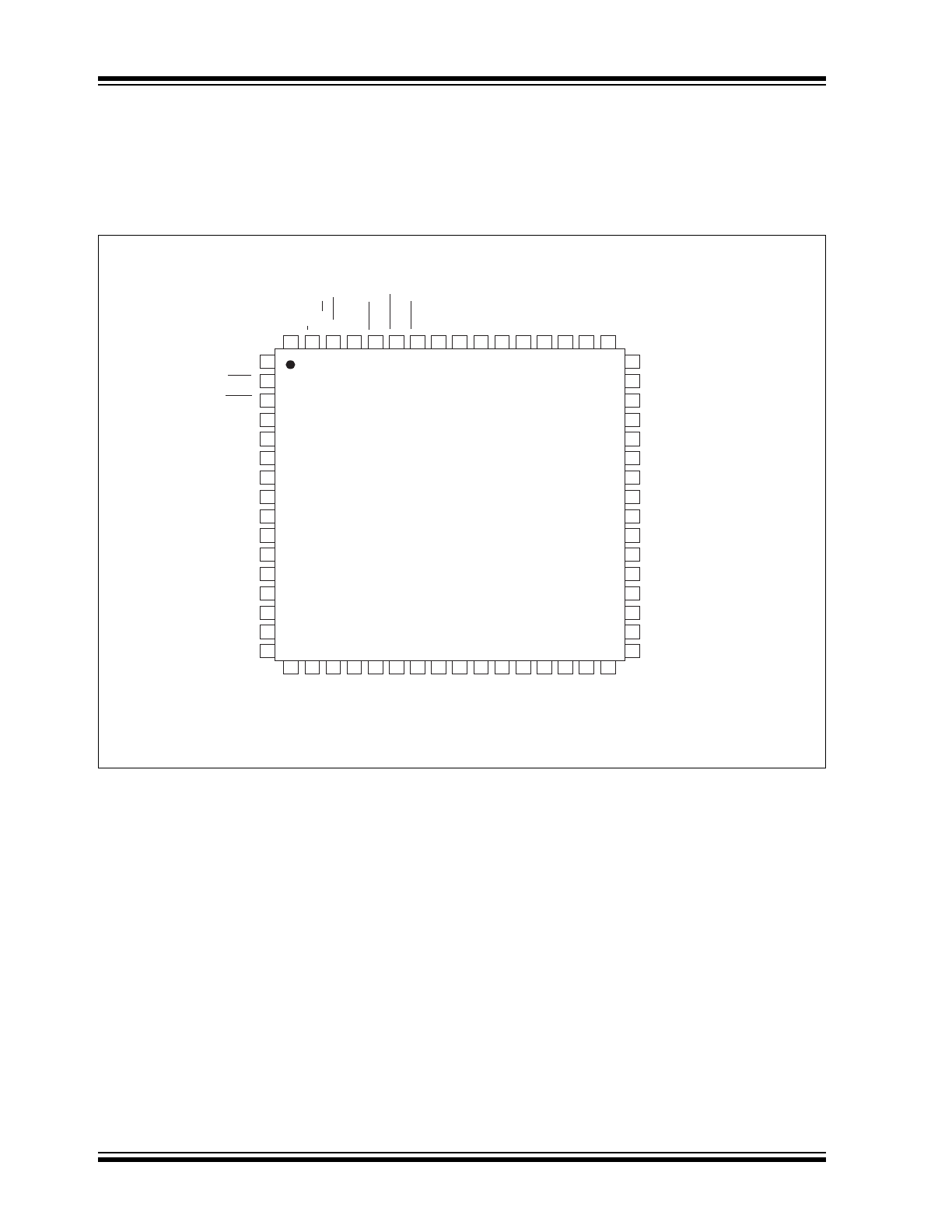
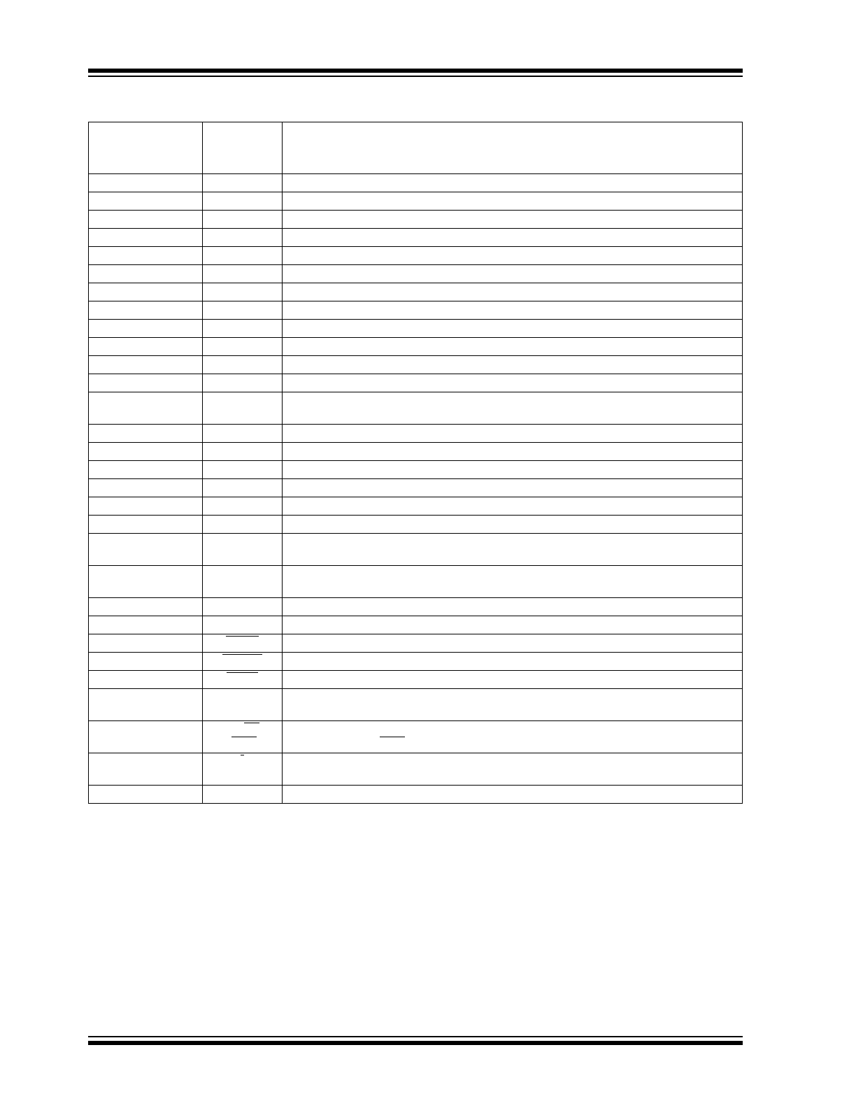
Package Type
47
52
51
50
49
64
63
62
58
57
56
55
54
53
60
59
24
25
26
27
28
29
30
18
19
20
21
22
23
32
17
1
2
3
4
5
6
7
8
9
10
11
12
13
14
15
45
44
43
42
41
40
39
38
37
36
35
34
33
48
TC815
C
REFL
RM
REFH
ANALOG COM
V
CC
AC/–/AUTO
BCP3
V
SSD
FE2
AGD2
-MEM/BATT
BCP2
FE1
AGD1
BCP1
16
OHM
20mA
BUZ
FE0
AGD0
BCP0
XTAL1
XTAL2
V
DISP
BP1
BP2
BP3
LO
Ω/A
Ω/V
k/m/
HOLD
NC
46
ΩR1
ΩR4
ΩR2
ΩR3
C
I
ACVL
I
I
C
REFH
REFHI
V
I
VR4
VR5
VR2
VR3
ΩR5
NC
61
31
NC
RM
REFL
R
X
CFI
AD1
AD0
R
Ω
BUF
RVIBUF
ACVH
V
SSA
DGND
RANGE
-MEM
I
HOLD
C
AZ
NC
DC/AC
Ω
/LOW
Ω
64-Pin PQFP
©
2005 Microchip Technology Inc.
DS21474C-page 3
TC815
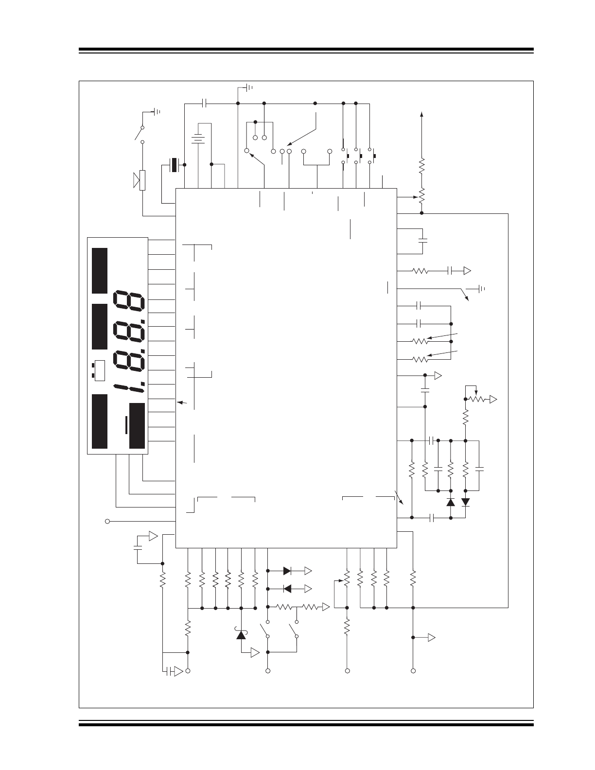
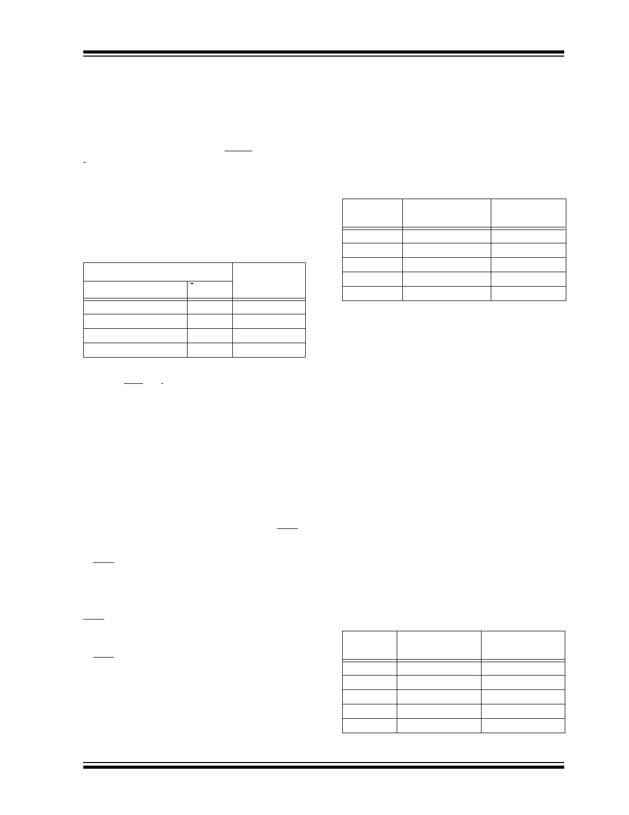
Typical Application and Test Circuit
-MEM
AUTO
HOLD
LO
kΩ
mVA
AC
– +
11
50
7
8
9
10
12
13
25
31
39
26
24
23
22
21
20
19
18
16
15
14
R6/100k
Ω
R7/100k
Ω
R8/220
Ω
(PTC)
Positive
Temperature
Coefficient
Resistor
R5/1.6385M
Ω
38
R4/163.85k
Ω
37
R3/16.385k
Ω
36
R2/1638.5
Ω
35
45
44
41
40
42
53
52
56
46
54
55
49
47
60
51
32
33
29
34
ADI
ACVH
ACVL
RΩ
BUF
RVIBUF
C
AZ
INT
HOLD
CIF
C
REFL
C
REFH
ANALOG
COM
REFHI
30
61
59
62
63
2
3
58
27
57
28
6
RM
REFH
-MEM
Manual RANGE Change
DC/AC or
Ω
/LOW
Ω
I
OHMS
20mA
Digital GND
V
SSD
V
SSA
V
CC
XTAL1
BUZ
XTAL2
5
4
43
V
I
(÷1)
V
R2
(÷10)
V
R3
(÷100)
V
R4
(÷1,000)
V
R5
(÷10,000)
ADO
R1/163.85
R14/9.9M
Ω
R12/1.11M
Ω
R11/101k
Ω
R10/10k
Ω
R9/1k
Ω
R13
500k
Ω
Z1
6.2V
20mA
200mA
Current
Input
Voltage
Input
Common
0.01
µF
Ohms
Input
0.1µF
If LCD Bias is Connected to DIG GND,
Peak Drive Signal
≈
5V.
LCD Bias
Tri-Plex
LCD Display
Segment & Decimal Point Drive
1's
10's
100's
1000's
Display
Annunciators
Backplane
Drivers
Ohms Range Attenuator
RMREFL
Ω
R5 (÷ 10,000)
Ω
R4 (÷ 1,000)
Ω
R3 (÷ 100)
Ω
R2 (÷ 10)
R1 (÷ 1)
I I
RX
VDISP
BP1
BP2
BP3
LO
Ω
/A
Ω
V
K/m
HOLD
AC/–/AUTO
-MEM/
BATT
BCP3
BCP2
FE2
AGD2
BCP1
FE1
AGD1
BCP0
FE0
AGD0
R15
9Ω
R16
1Ω
D3
D4
Enable
Audio
Transducer
32.768kHz
( 33kHz)
9V
+–
39pf
V
V
Ω
Ω
20mA
20mA
200mA
200mA
SIB
SIA
To V
CC
153.850mV
R19/5k
Ω
R18/24k
Ω
C
REF
0.1µF
R20
100
kΩ
C6
0.01µF
C
INT
C
AZ
150
kΩ
200
kΩ
0.1µF
0.1µF
R
Ω
BUF
RVIBUF
R26/3k
Ω
R24/10k
Ω
R23/10k
Ω
R22/470k
Ω
R21/2.2M
Ω
C4/µf
4.7µf
C2/0.22µF
R27/2k
Ω
C1/1µF
C5/1µf –+
–+
D1
D2
Voltage Range Attenuator
*Not Required when Resistor Network is used.
TC815
3-1/2 Digit Auto-Ranging DMM
with HOLD Function
TC815
DS21474C-page 4
©
2005 Microchip Technology Inc.
1.0
ELECTRICAL
CHARACTERISTICS
Absolute Maximum Ratings*
Supply Voltage (V+ to V–)
.....................................15V
Analog Input Voltage (Either Input) ................ V+ to V-
Reference Input Voltage.................................. V+ to V-
Voltage at Pin 45 ........................................ GND ±0.7V
Power Dissipation (T
A
≤
70°C)
64-Pin Plastic Flat Package ...........................1.14W
Operating Temperature Range:
Commercial Package (C) .................... 0°C to +70°C
Storage Temperature Range ..............-65°C to +150°C
*Stresses above those listed under "Absolute Maximum
Ratings" may cause permanent damage to the device. These
are stress ratings only and functional operation of the device
at these or any other conditions above those indicated in the
operation sections of the specifications is not implied.
Exposure to Absolute Maximum Rating conditions for
extended periods may affect device reliability.
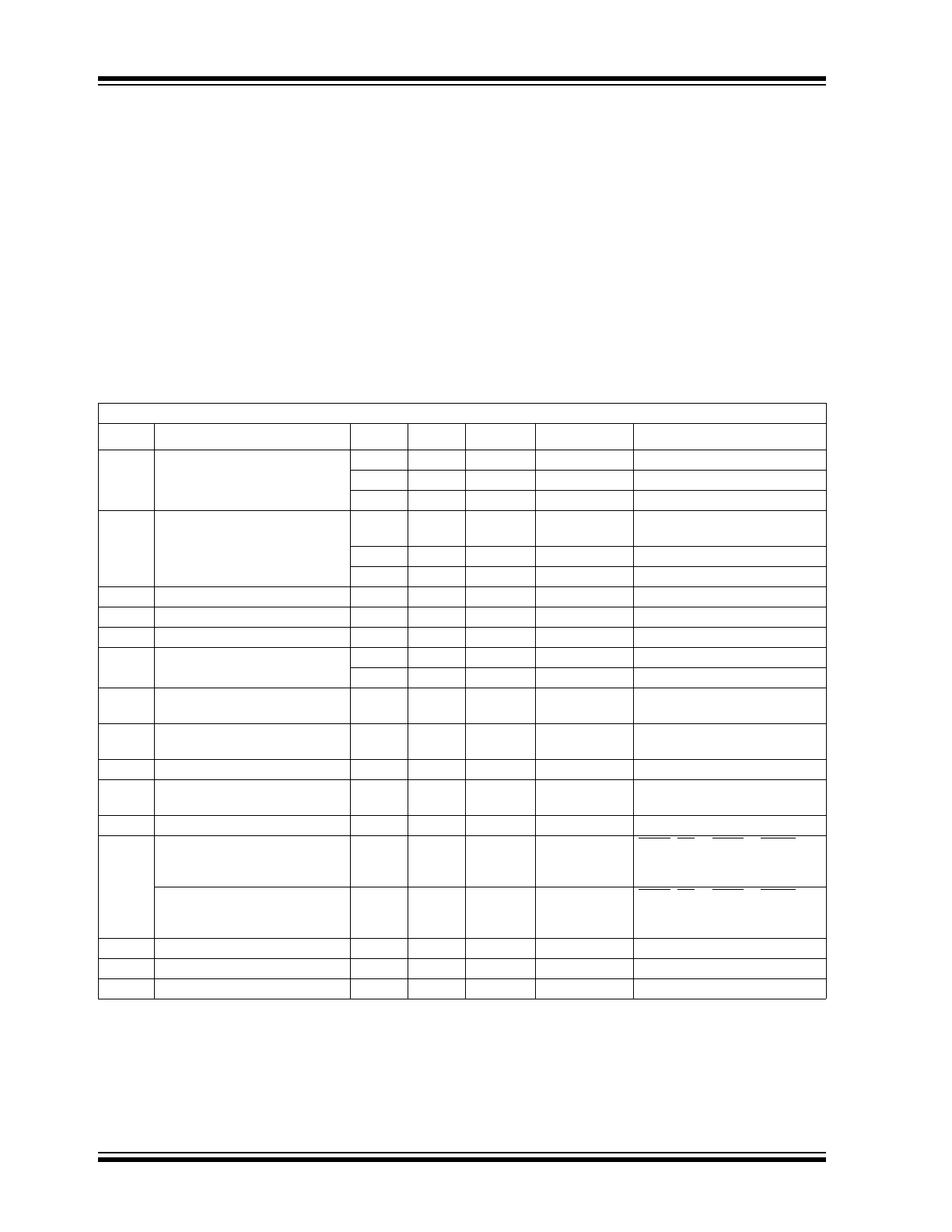
TC815 ELECTRICAL SPECIFICATIONS
Electrical Characteristics: V
A
= 9V, T
A
= +25°C, unless otherwise specified (see Typical Application and Test Circuit Figure).
Symbol
Parameter
Min
Typ
Max
Unit
Test Conditions
Zero Input Reading Input Resistor
-0000
0000
+0000
Digital Reading
200mV Range w/o 10M
Ω
Input
-0001
—
+0001
Digital Reading
200mV Range w/10M
Ω
Input
-0000
0000
+0000
Digital Reading
20mA and 200mA Range
RE
Rollover Error
—
—
±1 Count
200mV Range w/o 10M
Ω
Input Resistor
—
—
±3
200mV Range w/10M
Ω
Input
—
—
±1
20mA and 200mA Range
NL
Linearity Error
—
—
±1
Count
Best Case Straight Line
I
IN
Input Leakage Current
—
—
10
pA
E
N
Input Noise
—
20
—
μ
V
p-p
BW = 0.1 to 10Hz
AC Frequency Error
—
±1
—
%
40Hz to 500Hz
—
±5
—
%
40Hz to 200Hz
Open Circuit Voltage
—
570
660
mV
Excludes 200
Ω
Range
for OHM Measurements
Open Circuit Voltage
—
285
350
mV
Excludes 200
Ω
Range
for LO OHM Measurement
V
COM
Analog Common Voltage
2.5
2.6
3.3
V
(V
+
- V
COM
)
V
CTC
Common Voltage Temperature
Coefficient
—
—
50
ppm/°C
Display Multiplex Rate
—
100
—
Hz
V
IL
Low Logic Input
—
—
1
V
20mA, AC, I, LOW
Ω
, HOLD
Range, -MEM, OHMs
(Relative to DGND Pin 58)
Logic 1 Pull-up Current
—
25
—
μ
A
20mA, AC, I, LOW
Ω
, HOLD
Range, -MEM, OHMs
(Relative to DGND Pin 58)
Buzzer Drive Frequency
—
4
—
kHz
Low Battery Flag Voltage
6.3
6.6
7.0
V
V
CC
to V
SSA
Operating Supply Current
—
0.8
1.5
mA
©
2005 Microchip Technology Inc.
DS21474C-page 5
TC815
2.0
PIN DESCRIPTIONS
The descriptions of the pins are listed in Table 2-1.
TABLE 2-1:
PIN FUNCTION TABLE
Pin Number
(64-Pin Plastic)
Quad Flat Package
Symbol
Description
1
NC
Logic Input. “0” (Digital Ground) for resistance measurement.
2
OHM
Logic Input. “0” (Digital Ground) for 20mA full scale current measurement.
3
20mA
Audio frequency, 4kHz, output for continuity indication during resistance measurement.
4
BUZ
Audio frequency, 4kHz, output for continuity indication during resistance measurement. A
non-continuous 4kHz signal is output to indicate an input overrange during voltage or
current measurements.
5
XTAL1
32.768kHz Crystal Connection.
6
XTAL2
32.768kHz Crystal Connection.
7
V
DISP
Sets peak LCD drive signal: V
P
- V
DD
- V
DISP
. V
DISP
may also be used to compensate for
temperature variation of LCD crystal threshold voltage.
8
BP1
LCD Backplane #1.
9
BP2
LCD Backplane #2.
10
BP3
LCD Backplane #3.
11
LO
Ω
/A
LCD Annunciator segment drive for low ohms resistance measurement and current
measurement.
12
Ω
/V
LCD Annunciator segment drive for resistance measurement and voltage measurement.
13
k/m/HOLD
LCD Annunciator segment drive for k (“kilo-ohms”), m (“milliamps” and
“millivolts”) and HOLD mode.
14
BCP0
(One’s digit)
LCD segment drive for “b,” “c” segments and decimal point of least significant digit (LSD).
15
ADG0
LCD segment drive for “a,” “g,” “d” segments of LSD.
16
FE0
LCD segment drive for “f” and “e” segments of LSD.
17
NC
No connection.
18
BCP1
LCD segment drive for “b,” “c” segments and decimal point of 2nd LSD.
19
AGD1
LCD segment drive for “a,” “g,” “d” segments of 2nd LSD (Ten’s digit).
20
FE1
LCD segment drive for “f” and “e” segments of 2nd LSD.
21
BCP2
LCD segment drive for “b,” “c” segments and decimal point of 3rd LSD
(Hundred’s digit).
22
AGD2
LCD segment drive for “a,” “g,” “d” segments of 3rd LSD.
23
FE2
LCD segment drive for “b,” “c” segments and decimal point of 3rd LSD.
24
BCP3
LCD segment drive for “b,” “c” segments and decimal point of MSD
(Thousand’s digit).
25
AC/-/AUTO
LCD annunciator drive signal for AC measurements, polarity, and auto-range operation.
26
-MEM/BATT
LCD annunciator drive signal for low battery indication and Memory
(Relative Measurement) mode.
27
V
SSD
Negative battery supply connection for internal digital circuits. Connect to negative terminal
of battery.
28
V
CC
Positive battery supply connection.
29
ANALOG
COM
Analog circuit ground reference point. Nominally 2.6V below V
CC
.
30
RM
REFH
Ratiometric (Resistance measurement) reference high voltage.
31
RM
REFL
Ratiometric (Resistance measurement) reference low voltage.
32
C
REFL
Reference capacitor negative terminal C
REF
0.1µf.
33
C
REFH
Reference capacitor positive terminal C
REF
0.1µf.
34
REFHI
Reference voltage for voltage and current measurement; nominally 163.85mV.
TC815
DS21474C-page 6
©
2005 Microchip Technology Inc.
35
Ω
R1
Standard resistor connection for 200
Ω
full scale.
36
Ω
R2
Standard resistor connection for 2000
Ω
full scale.
37
Ω
R3
Standard resistor connection for 20k
Ω
full scale range.
38
Ω
R4
Standard resistor connection for 200k
Ω
full scale range.
39
Ω
R5
Standard resistor connection for 2000k
Ω
full scale range.
40
VR3
Voltage measurement ÷ 100 attenuator.
41
VR2
Voltage measurement ÷ 10 attenuator.
42
VR5
Voltage measurement ÷ 10,000 attenuator.
43
VR4
Voltage measurement ÷ 1000 attenuator.
44
V
I
Unknown voltage input ÷ 1 attenuator.
45
I
I
Unknown current input.
46
ACVL
Low output of AC to DC converter.
47
C
I
Integrator capacitor connection. Nominally 0.1µf. (Low dielectric absorption. Polypropylene
dielectrics suggested.)
48
NC
No connection.
49
C
AZ
Auto-zero capacitor connection; nominally 0.1µf.
50
R
X
Unknown resistance input.
51
CFI
Input filter connection.
52
AD1
Negative input of internal AC to DC operational amplifier.
53
AD0
Output of internal AC to DC operational amplifier.
54
R
Ω
BUF
Active buffer output for resistance measurement. Integration resistor connection. Integrator
resistor nominally 220k
Ω
.
55
RVIBUF
Active buffer output for voltage and current measurement. Integration resistor connection.
Integration resistor nominally 150k
Ω
.
56
ACVH
Positive output of AC to DC converter.
57
V
SSA
Negative supply connection for analog circuits. Connect to negative terminal of 9V battery.
58
DGND
Internal logic digital ground. The logic “0” level. Nominally 4.7V below V
CC
.
59
RANGE
Input to set manual operation and change ranges.
60
HOLD
Input to hold display. Connect to DIG GND.
61
-MEM
Input to enter Memory Measurement mode for relative measurements. The two LSD’s are
stored and subtracted from future measurements.
62
DS/AC
Ω
/LOW
Ω
Input that selects AC or DC option during voltage/current measurements. For resistance
measurements,
Ω/
LOW
Ω
,
the ohms or low power (voltage) ohms option can be selected.
63
I
Input to select current measurement. Set to logic “0” (Digital ground) for
current measurement
64
NC
No connection.
TABLE 2-1:
PIN FUNCTION TABLE (CONTINUED)
Pin Number
(64-Pin Plastic)
Quad Flat Package
Symbol
Description
©
2005 Microchip Technology Inc.
DS21474C-page 7
TC815
3.0
DETAILED DESCRIPTION
3.1
Resistance, Voltage, Current
Measurement Selection
The TC815 is designed to measure voltage, current,
and resistance. Auto-ranging is available for resistance
and voltage measurements. The OHMS (Pin 2) and
I (Pin 63) input controls are normally pulled internally to
V
CC.
By tying these pins to Digital Ground (Pin 58), the
TC815 is configured internally to measure resistance,
voltage, or current. The required signal combinations
are shown in Table 3-1.
TABLE 3-1:
MEASUREMENT SELECTION
LOGIC
Note
1:
0 = Digital Ground
2: 1 = Floating or Tied to V
CC
3: OHM and I are normally pulled internally high to
V
CC
(Pin 28). This is considered a logic “1.”
4: Logic “0” is the potential at digital ground (Pin 58).
3.2
Resistance Measurements
(Ohms and Low Power Ohms)
The TC815 can be configured to reliably measure in-
circuit resistances shunted by semiconductor junc-
tions. The TC815 Low Power Ohms Measurement
mode limits the probe open circuit voltage. This pre-
vents semiconductor junctions in the measured system
from turning on.
In the Resistance Measurement mode, the
Ω
/LOW
Ω
(Pin 62) input selects the Low Power Ohms Measure-
ment mode. For low power ohms measurements,
Ω
/LOW
Ω
(Pin 62) is momentarily brought low to digital
ground potential. The TC815 sets up for a low power
ohms measurement with a maximum open circuit
probe voltage of 0.35V above analog common. In the
Low Power Ohms mode, an LCD display annunciator,
LOW
Ω
, will be activated. On power-up, the Low Power
Ohms mode is not active.
If the Manual mode has been selected, toggling
Ω
/LOW
Ω
will reset the TC815 back to the Auto-Range
mode. In Manual mode, the decision to make a normal
or low power ohms measurement should be made
before selecting the desired range.
The low power ohms measurement is not available on
the 100
Ω
full scale range. Open circuit voltage on this
range is below 2.8V. The standard resistance values
are listed in Table 3-2.
R8, a positive temperature coefficient resistor, and the
6.2V zener Z1 in Figure 3-1, provide input voltage pro-
tection during ohms measurements.
TABLE 3-2:
OHMS RANGE LADDER
NETWORK
3.3
Ratiometric Resistance
Measurements
The TC815 measures resistance ratiometrically. Accu-
racy is set by the external standard resistors connected
to Pin 35 through 39. A Low Power Ohms mode may
be selected on all but the 200
Ω
full scale range. The
Low Power Ohms mode limits the voltage applied to the
measured system. This allows accurate “in-circuit”
measurements when a resistor is shunted by semicon-
ductor junctions. Full auto-ranging is provided. External
precision standard resistors are automatically switched
to provide the proper range.
Figure 3-1 shows a detailed block diagram of the
TC815 configured for ratiometric resistance measure-
ments. During the signal integrate phase, the reference
capacitor charges to a voltage inversely proportional to
the measured resistance, R
X
. Figure 3-2 shows the
conversion accuracy relies on the accuracy of the
external standard resistors only.
Normally the required accuracy of the standard resis-
tances will be dictated by the accuracy specifications of
the users end product. Table 3-3 gives the equivalent
ohms per count for various full scale ranges to allow
users to judge the required resistor for accuracy.
TABLE 3-3:
REFERENCE RESISTORS
Function Select Pin
Selected
Measurement
OHM (Pin 2)
I (Pin 63)
0
0
Voltage
0
1
Resistance
1
0
Current
1
1
Voltage
Full Scale
Range
Standard
Resistance
Low Power
Ohms Mode
200
Ω
163.85
Ω
(R1)
NO
2000
Ω
1638.5 k
Ω
(R2)
YES
20k
Ω
16,385
Ω
(R3)
YES
200k
Ω
16385
Ω
(R4)
YES
2,000k
Ω
1,638,500
Ω
(R5)
YES
Full Scale
Range
Reference
Resistor
Ω
/Count
200k
163.85
0.1
2k
1638.5
1
20k
16385
10
200k
163850
100
2M
1638500
1000
TC815
DS21474C-page 8
©
2005 Microchip Technology Inc.
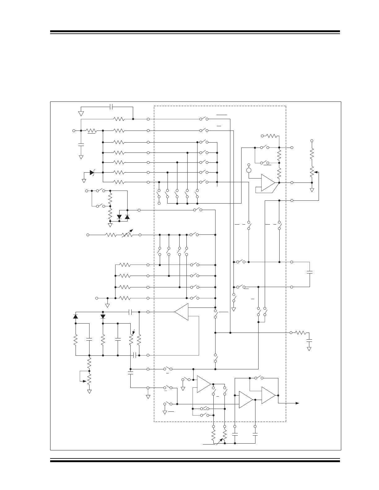
FIGURE 3-1:
RATIOMETRIC RESISTANCE MEASUREMENT FUNCTIONAL DIAGRAM
FIGURE 3-2:
RESISTANCE MEASUREMENT ACCURACY SET BY EXTERNAL
STANDARD RESISTOR
Buffer
TC815
R6/100k
Ω
50
32
S19
DE
S20
V
CC
- 2.6V
1.5kV
V
CC
Low Ohms
HI
Ohms
VA
S29
S30
S31
S32
S33
÷1
÷10
÷100
÷1k
÷10k
S28
S27
S26
S25
S24
DE
S23
Voltage
Reference
39
38
37
36
35
÷1
÷10
÷100
÷1k
÷10k
Integrator
Comparator
S37
S35
55
54
R
ΩBUF
S12
S13
DE
S18
S21
DE
INT • (
Ω + DC)
33
C
REF
0.1µF
R7/100k
31
Analog
Common
29
34
28
10k
Ω
57
30
30
V
SSA
9V
R18
24k
Ω
5k
Ω
REFHI
220k
Ω
49
0.1µF
150k
Ω
RVIBUF
47
C
INT
0.1µF
S36
S34
R
X
Unknown
R8
220
Ω
V •
1
1
R5/1638500
Ω
R4/163850
Ω
R3/16385
Ω
R2/1638.5
Ω
R1/163.85
Ω
DE +
Ω
• LO
C
AZ
V
CC
- 2.8V
≈
V
SSD
V
CC
~
1.5k
Ω
~
•
•
•
DE
•
Ω
•
•
50
Ω
Ω
Ω
Ω
Ω
Ω
Ω
Ω
Ω
+
–
Example: 200k
Ω
Full Scale Measurement
V
R
163.85k
Ω
163.85
220
R
X
+
+
-------------------------------------------------
⎝
⎠
⎛
⎞
x0.64
=
(a )
(b)
V
X
R
X
163.85k
Ω
220
Ω
R
X
+
+
--------------------------------------------------------------
⎝
⎠
⎛
⎞
x0.64
=
(c) “Ramp Up Voltage” = “Ramp Down Voltage”
V
X
R
I
C
I
(
)
----------------xT
I
V
X
R
I
C
I
(
)
----------------T
DE
=
.
. .
Where:
R
I
= Integrating Resistor, T
I
= Integrate Time
C
I
= Integrating Capacitor, T
DE =
Deintegrate Time
(d)
R
X
= 163.85
T
I
(T
DE
)
Independent of R
I
, C
I
or Internal Voltage Reference
Unknown
R
X
220
Ω
0.64V for Ohms
0.32V for LO Ohms
To Analog Buffer
V
X
V
R
C
REF
100 k
Ω
R
S
16.385k
+
V
R
VA
©
2005 Microchip Technology Inc.
DS21474C-page 9
TC815
3.4
Voltage Measurement
Resistive dividers are automatically changed to provide
in range readings for 200mV to 2000V full scale readings
(Figure 3-3). The input resistance is set by external
resistors R14/R13. The divider leg resistors are R9-R12.
The divider leg resistors give a 200mV signal V
I
(Pin 44) for full scale voltages from 200mV to 2000V.
For applications which do not require a 10m
Ω
input
impedance, the divider network impedances may be
lowered. This will reduce voltage offset errors induced
by switch leakage currents.
FIGURE 3-3:
TC815 ANALOG SECTION
TC815
+
–
2.8V REF AMP
10k
Ω
V
CC
1.5k
S43
V
CC
R18/24k
V
CC
R19/5k
ANALOG
COM
29
REFHI
RM
REFH
163.85mV
≈
0.1µF
C
REFH
51 CIF
0.01µF
C6
R20/100k
Ω
To Digital
Section
S38 AZ
Comparator
Integrator
49
47
INT
0.01µF
0.01µF
C
INT
55
RVI
BUF
150
k
54
R
BUF
220
k
RBUF
RBUF
S34
DE •
S20 DE
S18 DE
S19 DE+
S16 DE+
S17 DE-
Buffer
S35
S37
INT+ +DC
C1/1µF
0.22 µF
ACVH
S15 AZ
4
3
2
1
39
38
37
36
35
31
50
R7/100k
Ω
R6/100k
Ω
R5/1.638M
Ω
R1/163.85
Ω
5
R4/163.85k
Ω
R3/16385
Ω
R2/1638.5
Ω
RM
REFL
ΩR
ΩR
ΩR
ΩR
ΩR
0.01µF
Ohms
Input
Current Input
R8/220
0.1µF
(PTC)
D3
6.2V
200mA
D4
R15/9
20mA
R16/1
I 45
I
R12/1.11M
R11/101k
R10/10k
R9/1k
ACVL 46
R24
10k
R23
10k
Ω
R26
33k
Ω
R27/2k
Ω
Common
D2
C3
1µF
C4
1µF
V 44
I
V
R2
41
V
R3
40
V
R4
43
V
R2
42
ADO
ADI
Voltage
Input
R22
470
k
R21
2.2
M
R14/9.9M
Ω
R13/500k
Ω*
4.7µF
Z1
S28
S27
S26
S25
S21 DE •
S12 V • 1/1
1/1k
•
1/100
•
1/10
•
1/1
•
+AC
INT•( +DC)
S11
S13
AC-to-DC
Converter
Op Amp
V•1/1
V•1/10
V•1/100
V•1/1k
V•1/10k
1/10 1/100 1/1k
1/10k
S32
S33
S31
S30
S29
1/1
•
CC
V
S10
+ 1
S6
S7
S8 S9
S1
S2
S3
S4
S5
*Not required when
Resistor Network is used.
INT• •AC
V•
1/10
V•
1/100
V•
1/1
k
V•
1/10k
D1
DE
33 C
REFH
32 C
REFL
C
AZ
+
+
53
S24
1/10k
•
•
•
•
•
C
AZ
S44
HI
•
•
S14
S40
INT• •AC
LO
•
52
56
S22
S22
C2
S39
1.5k
Ω
Ω
Ω
Ω
Ω
Ω
W
Ω
Ω
Ω
Ω
Ω
Ω
Ω
Ω
Ω
W
Ω
Ω
Ω
Ω
Ω
Ω
Ω
Ω
Ω
Ω
Ω
Ω
Ω
Ω
Ω
Ω
Ω
Ω
Ω
Ω
Ω
Ω
Ω
Ω
Ω
Ω
W
Ω
+
–
+
–
+
–
+
–
+
–
34
30
ΩR
X

TC815
DS21474C-page 10
©
2005 Microchip Technology Inc.
3.5
Current Measurement
The TC815 measures current only under manual range
operation. The two user selectable full scale ranges
are: 20mA and 200mA. Select the current Measure-
ment mode by holding the I input (Pin 63) low at digital
ground potential. The OHM input (Pin 2) is left floating
or tied to the positive supply.
Two ranges are possible. The 20mA full scale range is
selected by connecting the 20mA input (Pin 3) to digital
ground. If left floating the 200mA full scale range is
selected.
External current to voltage conversion resistors are
used at the I
I
input (Pin 45). For 20mA measurements
a 10
Ω
resistor is used. The 200mA range needs a 1
Ω
resistor; full scale is 200mV.
PC board trace resistance between analog common
and R16 (see Figure 2-1) must be minimized. In the
200mA range, for example, a 0.05 trace resistance will
cause a 5% current to voltage conversion error at I
I
(Pin 45).
The extended resolution measurement option operates
during current measurements. To minimize rollover
error the potential difference between ANALOG COM
(Pin 29) and system common must be minimized.
3.6
Measurement Options
(AC to DC Measurements)
In voltage and current measurements, the TC815 can
be configured for AC measurements. An on-chip oper-
ational amplifier and external rectifier components per-
form the AC to DC conversion.
When power is first applied, the TC815 enters the DC
Measurement mode. For AC measurements (current or
voltage), AC/DC (Pin 62) is momentarily brought low to
digital ground potential; the TC815 sets-up for AC mea-
surements and the AC liquid crystal display annuncia-
tor activates. Toggling AC/DC low again will return the
TC815 to DC operation.
If the Manual Operating mode has been selected, tog-
gling AC/DC will reset the TC815 back to the Auto-
Range mode. In Manual mode operation, AC or DC
operation should be selected first and then the desired
range selected.
The minimum AC voltage full scale voltage range is 2V.
The DC full scale minimum voltage is 200mV. AC cur-
rent measurements are available on the 20mA and
100mA full scale current ranges.