
2001-2012 Microchip Technology Inc.
DS21438C-page 1
TC59
Features
• Low Dropout Voltage
- Typically 120mV @ 50mA; 380mV @ 100mA
for -5.0V Output Part
• Tight Output Voltage Tolerance: ±2% Max
• Low Supply Current: 3.5
A, Typ
• Small Package: 3-Pin SOT-23A
Applications
• Cellular Phones
• Battery Operated Systems
• Palmtops
• Portable Cameras
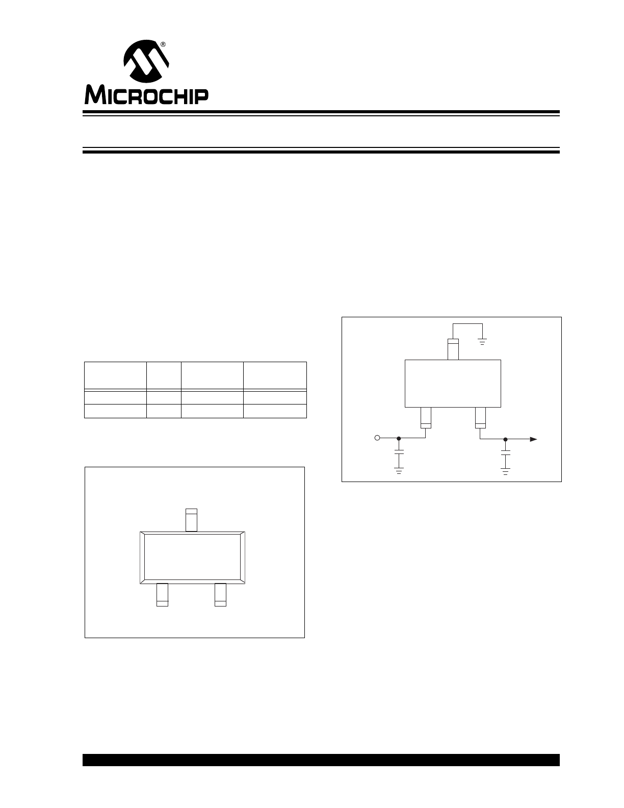
Device Selection Table
Other output voltages are available. Please contact Microchip
Technology Inc. for details.
Package Type
General Description
The TC59 is a low dropout, negative output voltage
regulator designed specifically for battery-operated
systems. Its full CMOS construction eliminates the
wasted ground current typical of bipolar LDOs. This
reduced supply current significantly extends battery
life, particularly when the TC59 is operated in dropout.
Other TC59 key features include low supply current
(typically 3.0
A) and low dropout operation (typically
120mV at 50mA). The TC59 is packaged in a small
3-Pin SOT-23A package.
Functional Block Diagram
Part Number
Output
Voltage
Package
Temperature
Range
TC593002ECB
3.0V
3-Pin SOT-23A -40°C to +85°C
TC595002ECB
5.0V
3-Pin SOT-23A -40°C to +85°C
V
SS
3-Pin SOT-23A
TC59
1
4
2
-V
IN
-V
OUT
NOTE: 3-Pin SOT-23A is equivalent to the EIAJ SC59
-V
IN
1
µ
F
1
µ
F
-V
OUT
-V
OUT
TC59
1
2
3
-V
IN
V
SS
+
+
_
_
Low Dropout, Negative Output Voltage Regulator
TC59
DS21438C-page 2
2001-2012 Microchip Technology Inc.
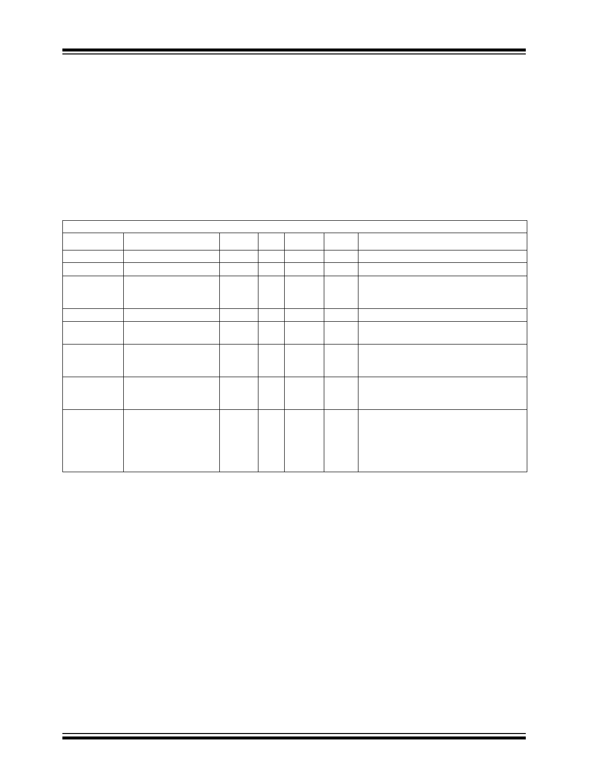
1.0
ELECTRICAL
CHARACTERISTICS
Absolute Maximum Ratings*
Input Voltage .........................................................-12V
Output Current ..................................................200mA
Output Voltage..................... -V
DD
– 0.3V to V
IN
+ 0.3V
Power Dissipation.............................................150mW
Operating Temperature Range............. -40°C to +85°C
Storage Temperature Range ..............-40°C to +125°C
Stresses above those listed under "Absolute Maximum
Ratings" may cause permanent damage to the device. These
are stress ratings only and functional operation of the device
at these or any other conditions above those indicated in the
operation sections of the specifications is not implied.
Exposure to Absolute Maximum Rating conditions for
extended periods may affect device reliability.
TC59 ELECTRICAL SPECIFICATIONS
Electrical Characteristics: V
IN
= V
R
– 1.0V (Note 1), C
L
= 10
F, T
A
= 25°C unless otherwise noted.
Symbol
Parameter
Min
Typ
Max
Units
Test Conditions
V
IN
Input Voltage
—
—
-10
V
I
OUT
= 20mA
I
DD
Supply Current
—
3
7
A
I
OUT(MAX)
Maximum Output Current
100
80
60
—
—
—
—
—
—
mA
mA
mA
V
IN
= -6.0V; V
R
= -5.0V, V
OUT
-4.5V
V
IN
= -5.0V; V
R
= -4.0V, V
OUT
-3.6V
V
IN
= -4.0V; V
R
= -3.0V, V
OUT
-2.7V
V
OUT
Output Voltage
1.02
X
V
R
—
0.98 x V
R
V
I
OUT
= 20mA
TC V
OUT
Output Voltage
Temperature Coefficient
—
±100
—
ppm/°C I
OUT
= 20mA
V
OUT
/
(
V
IN
X
V
OUT
)
Line Regulation
—
0.1
0.3
%/V
I
OUT
= 20mA; V
R
= -5.0V; -6.0 < V
IN
< -10.0V
V
R
= -4.0V; -5.0 < V
IN
< -10.0V
V
R
= -3.0V; -4.0 < V
IN
< -10.0V
V
OUT
Load Regulation
—
40
80
mV
V
R
= -5.0V; 1mA < I
OUT
< 50mA
V
R
= -4.0V; 1mA < I
OUT
< 45mA
V
R
= -3.0V; 1mA < I
OUT
< 40mA
V
IN
- V
OUT
Dropout Voltage
—
—
—
—
—
—
120
380
120
380
120
380
300
600
300
600
300
600
mV
mV
mV
mV
mV
mV
V
R
= -5.0V; I
OUT
= 50mA
I
OUT
= 100mA
V
R
= -4.0V; I
OUT
= 45mA
I
OUT
= 90mA
V
R
= -3.0V; I
OUT
= 40mA
I
OUT
= 80mA
Note
1:
V
R
is the regulator output voltage setting. For example: V
R
= -2.5V, -2.7V, -3.0V, -3.3V, -3.6V, -4.0V, -5.0V.
2001-2012 Microchip Technology Inc.
DS21438C-page 3
TC59
2.0
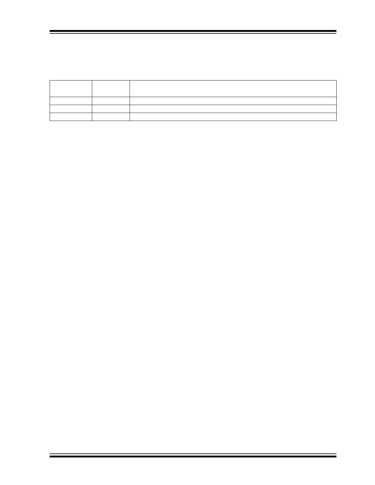
PIN DESCRIPTIONS
The descriptions of the pins are listed in Table 2-1.
TABLE 2-1:
PIN FUNCTION TABLE
3.0
DETAILED DESCRIPTION
The TC59 is a low quiescent current, precision fixed
negative output voltage LDO. Unlike bipolar linear
regulators, the TC59 supply current does not increase
proportionally with load current.
3.1
Output Capacitor
A minimum of 1
F tantalum output capacitor is
required. The requirements for the output capacitor are
an equivalent series resistance (esr) greater than 0.1
and less than 5
, with a self-resonant frequency
greater than 1MHz. To improve supply noise rejection
and transient response, larger output capacitors can be
used. Care should be taken when increasing C
OUT
, that
the input impedance is not high enough to cause high
input impedance oscillation.
3.2
Input Capacitor
A 1
F input capacitor is recommended for most
applications when the input impedance is on the order
of 10
. When operating off of a battery input, or there
is a large distance from the input source to the LDO,
larger input capacitance may be required for stability.
When large values of output capacitance are used, the
input capacitance should be increased to prevent high
source impedance oscillations.
Pin No.
(3-Pin SOT-23A)
Symbol
Description
1
V
OUT
Regulated voltage output.
2
V
IN
Supply voltage input.
3
V
SS
Ground.
TC59
DS21438C-page 4
2001-2012 Microchip Technology Inc.
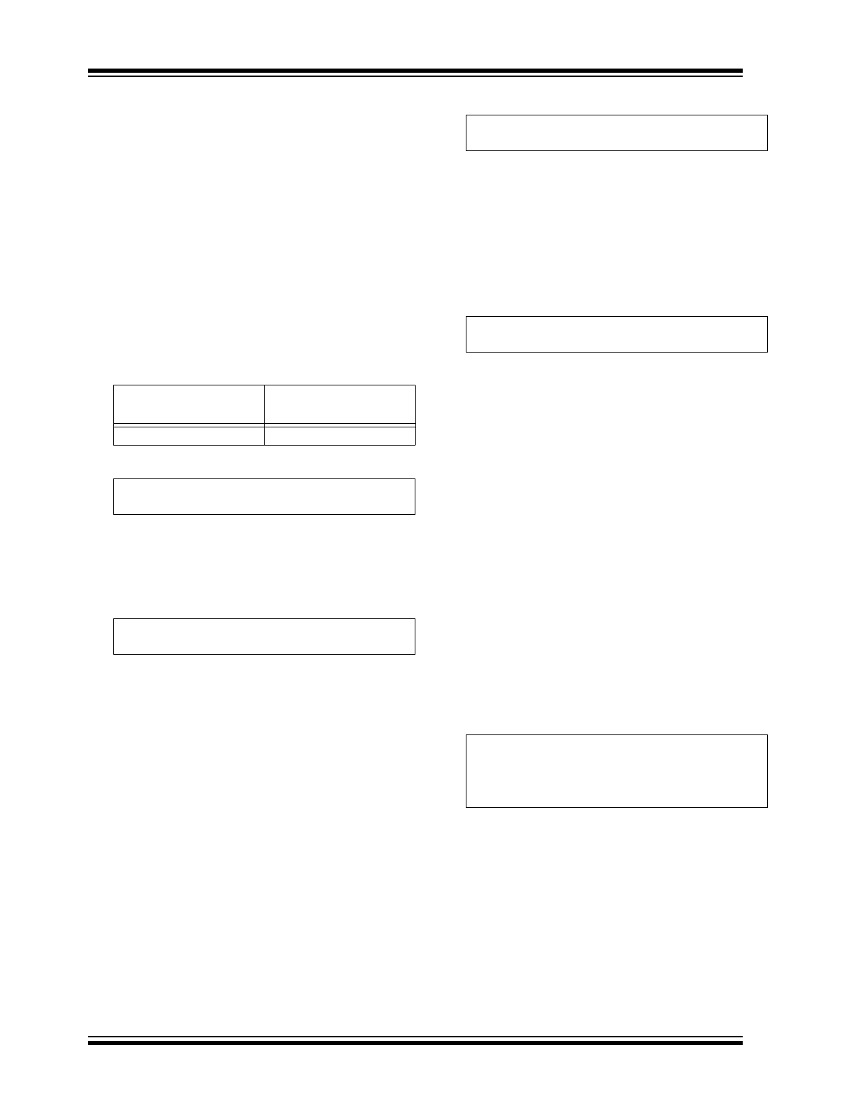
4.0
THERMAL CONSIDERATIONS
4.1
Power Dissipation
The amount of power dissipated internal to the low drop
out linear regulator is the sum of the power dissipation
within the linear pass device (P-Channel MOSFET),
and the quiescent current required to bias the internal
reference and error amplifier. The internal linear pass
device power dissipation is calculated multiplying the
voltage across the linear device times the current
through the device. The input and output voltages are
negative for the TC59. The power dissipation is
calculated using the absolute value of the voltage
difference between the input and output voltage.
TABLE 4-1:
MAXIMUM POWER
DISSIPATION
EQUATION 4-1:
The internal power dissipation as a result of the bias
current for the LDO internal reference and error
amplifier is calculated by multiplying the ground or
quiescent current times the input voltage.
EQUATION 4-2:
The total internal power dissipation is the sum of
Equation 4-1 and Equation 4-2.
EQUATION 4-3:
For the TC59, the internal quiescent bias current is so
low (3
A typical), the P
D
(Bias) term of the power
dissipation equation can be ignored. The maximum
power dissipation can be estimated by using the
maximum input voltage and the minimum output
voltage to obtain a maximum voltage differential
between input and output and multiplying the maximum
voltage differential by the maximum output current.
EQUATION 4-4:
For example, given the following conditions:
V
IN
= -7.0V ±5%
V
OUT
= -5.0V ±2%
I
OUT
= 1mA to 40mA
T
AMBIENT (MAX)
= 55°C
P
MAX
= (7V X (1.05) – (5.0V X 0.98)) X 40mA
P
MAX
= 98.0 milli-Watts
To determine the junction temperature of the device,
the thermal resistance from junction to air must be
known. The SOT-23-3 R
JA
is estimated to be
approximately 359°C/W when mounted on a 4-layer
board. The R
JA
will vary with physical layout, airflow
and other application specific conditions.
The device junction temperature is determined by
calculating the junction temperature rise above
ambient, then adding the rise to the ambient
temperature.
EQUATION 4-5:
JUNCTION
TEMPERATURE
(SOT-23 EXAMPLE)
Package Type
Maximum Power
Dissipation
SOT-23-3
150mW
P
D
(Pass Device) = (V
IN
– V
OUT
) X I
OUT
P
D
(Bias) = V
IN
X I
GND
P
TOTAL
= P
D
(Pass Device) + P
D
(Bias)
P
MAX
= (V
IN (MAX)
– V
OUT (MIN)
) X I
OUT (MAX)
T
JUNCTION
= P
D (MAX)
X R
JA
+ T
AMBIENT
T
JUNCTION
= 98.0 milli-Watts X 359°C/W + 55°C
T
JUNCTION
= 90.2°C
2001-2012 Microchip Technology Inc.
DS21438C-page 5
TC59
5.0
TYPICAL CHARACTERISTICS
Note:
The graphs and tables provided following this note are a statistical summary based on a limited number of
samples and are provided for informational purposes only. The performance characteristics listed herein are
not tested or guaranteed. In some graphs or tables, the data presented may be outside the specified
operating range (e.g., outside specified power supply range) and therefore outside the warranted range.
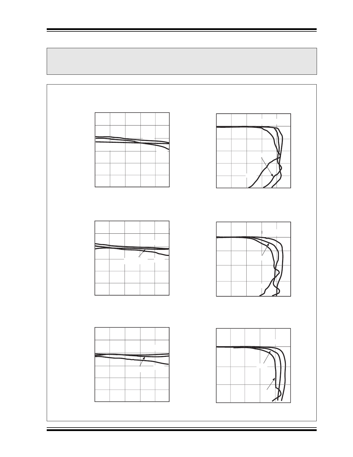
1. OUTPUT VOLTAGE vs. OUTPUT CURRENT
TC593002 (-3V)
TC593002 (-3V)
TC594002 (-4V)
-3.10
0
20
40
60 80 100
-5
0
-4.10
0
0
0
20
40
60
80
100
OUTPUT CURRENT I
OUT
(mA)
-5.10
-5.05
-5.00
-4.95
-4.90
-4.85
-4.80
TC595002 (-5V)
OUTPUT VOLTAGE V
OUT
(V)
-4.05
-4.00
-3.95
-3.90
-3.85
-3.80
0
20
40
60
80
100
-3.05
-3.00
-2.95
-2.90
-2.85
-2.80
0
-1
-2
-3
-4
-5
-6
0
50
100
150
200
250
-4
-3
-2
-1
0
50
100
150
200
250
-1
-2
-3
-4
50
100
150
200
250
T
T
OPR
= -40
°
C
C
25
°
C
80
°
C
T
OPR
= -40
°
C
25
°
C
80
°
C
T
OPR
= -40
°
C
C
25
°
C
V
IN
= -6.0V
T
T
OPR
= -40
°
C
C
25
°
C
80
°
C
T
T
T
OPR
= -40
°
C
C
25
°
C
80
°
C
T
T
OPR
= -40
°
C
C
25
°
C
80
°
C
80
°
C
OUTPUT CURRENT I
OUT
(mA)
TC595002 (-5V)
OU
TP
U
T V
O
LTA
G
E V
OU
T
(V
)
V
IN
= -6.0V
OUTPUT CURRENT I
OUT
(mA)
OUTPUT VOLTAGE V
OUT
(V)
V
IN
= -5.0V
TC594002 (-4V)
OUTPUT CURRENT I
OUT
(mA)
OU
TP
U
T V
O
LTA
G
E V
OU
T
(V
)
V
IN
= -5.0V
OUTPUT CURRENT I
OUT
(mA)
OUTPUT VOLTAGE V
OUT
(V)
V
IN
= -4.0V
OUTPUT CURRENT I
OUT
(mA)
OU
TP
U
T V
O
LTA
G
E V
OU
T
(V
)
V
IN
= -4.0V
TC59
DS21438C-page 6
2001-2012 Microchip Technology Inc.
5.0
TYPICAL CHARACTERISTICS (CONTINUED)
2. OUTPUT VOLTAGE vs. INPUT VOLTAGE
TC593002 (-3.0V
)
TC594002 (-4.0V)
-5
-6
-7
-8
-9
-10
INPUT VOLTAGE V
IN
(V)
OU
TP
U
T V
O
LTA
G
E V
OU
T
(V
)
TC595002 (-5.0V)
-4.2
-4.4
-4.6
-4.8
-5.0
-5.2
-4.5
-5.0
-5.5
-3.2
-3.4
-3.6
-3.8
-4.0
-4.2
-3.5
-4.0
-4.5
-2.2
-2.4
-2.6
-2.8
-3.0
-3.2
-4.85
-4.90
-4.95
-5.00
-5.05
-5.10
-4
-5
-6
-7
-8
-9
-3.85
-3.90
-3.95
-4.00
-4.05
-4.10
-10
-3
-4
-5
-6
-7
-8
-2.85
-2.90
-2.95
-3.00
-3.05
-3.10
-9
-10
20mA
40mA
T
OPR
= 25
°
C
-2.5
-3.0
-3.5
I
OUT
A
= 1mA
I
OUT
= 1mA
20mA
A
A
40mA
I
OUT
= 1mA
40mA
20mA
I
OUT
= 1mA
40mA
20mA
I
OUT
= 1mA
40mA
20mA
I
OUT
= 1mA
40mA
20mA
INPUT VOLTAGE V
IN
(V)
OUTPUT VOLTAGE V
OUT
(V)
TC595002 (-5.0V)
T
OPR
= 25
°
C
INPUT VOLTAGE V
IN
(V)
OUTPUT VOLTAGE V
OUT
(V)
T
OPR
= 25
°
C
TC594002 (-4.0V)
INPUT VOLTAGE V
IN
(V)
OU
TP
U
T V
O
LTA
G
E V
OU
T
(V
)
T
OPR
= 25
°
C
INPUT VOLTAGE V
IN
(V)
OUTPUT VOLTAGE V
OUT
(V)
T
OPR
= 25
°
C
TC593002 (-3.0V
)
INPUT VOLTAGE V
IN
(V)
OU
TP
U
T V
O
LTA
G
E V
OU
T
(V
)
T
OPR
= 25
°
C
2001-2012 Microchip Technology Inc.
DS21438C-page 7
TC59
5.0
TYPICAL CHARACTERISTICS (CONTINUED)
INPUT/OUTPUT VOLTAGE DIFF. V
DIF
(V)
TC595002 (-3.0V)
OUTPUT CURRENT I
OUT
(mA)
INP
U
T
/OU
TP
U
T V
O
LTA
G
E DIFF. V
DIF
(
V
)
TC595002 (-4.0V)
OUTPUT CURRENT I
OUT
(mA)
0
20
40
60
80
100
INPUT/OUTPUT VOLTAGE DIFF. V
DIF
(V)
TC595002 (-5.0V)
I
OUT
(mA)
0
200
400
600
800
0
40
80
0
200
400
600
800
0
40
100
0
200
400
600
800
3. INPUT/OUTPUT VOLTAGE DIFFERENTIAL vs. OUTPUT CURRENT
20
60
100
T
OPR
= 25
°
C
80
°
C
-40
°
C
20
80
60
T
OPR
= 25
°
C
80
°
C
-40
°
C
T
OPR
= 25
°
C
C
80
°
C
-40
°
C
INPUT VOLTAGE V
IN
(V)
SU
PPLY
CU
RRENT I
SS
(
µ
A)
INPUT VOLTAGE V
IN
(V)
SUPPLY CURRENT I
SS
(
µ
A)
4. SUPPLY CURRENT vs. INPUT VOLTAGE
TC595002 (-5.0V
)
0
1
2
3
4
5
-5
-6
-7
-8
-9
TC595002 (-5.0V)
1.5
2.0
2.5
3.0
3.5
4.0
-10
0
-6
-10
-2
-4
-8
T
OPR
= 25
°
C
80
°
C
-40
°
C
1.0
T
OPR
= 25
°
C
80
°
C
-40
°
C
TC59
DS21438C-page 8
2001-2012 Microchip Technology Inc.
5.0
TYPICAL CHARACTERISTICS (CONTINUED)
SUPPLY CURRENT I
SS
(
µ
A)
INPUT VOLTAGE V
IN
(V)
0
-2
-4
-6
-8
-10
TC594002 (-4.0V)
0
-2
-4
-6
-8
-10
TC593002 (-3.0V)
TC593002 (-3.0V)
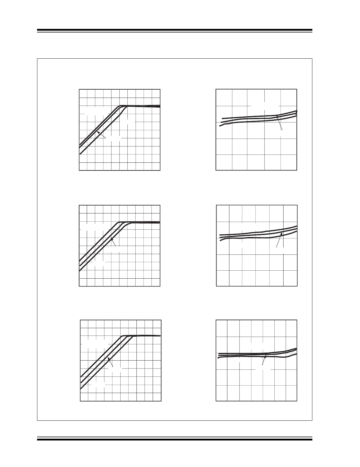
4. SUPPLY CURRENT vs. INPUT VOLTAGE (CONTINUED)
0
1
2
3
4
5
-4
-5
-6
-7
-8
-9
TC594002 (-4.0V)
-10
T
OPR
= 25
°
C
80
°
C
-40
°
C
4.0
3.5
3.0
2.5
2.0
1.5
1.0
T
OPR
= 25
°
C
80
°
C
-40
°
C
4.0
1.0
1.5
2.0
2.5
3.0
3.5
-3
-4
-5
-6
-7
-8
-9
-10
T
OPR
= 25
°
C
80
°
C
-40
°
C
0
1
2
3
4
5
T
OPR
= 25
°
C
80
°
C
-40
°
C
SUPPLY CURRENT I
SS
(
µ
A)
INPUT VOLTAGE V
IN
(V)
SUPPLY CURRENT I
SS
(
µ
A)
INPUT VOLTAGE V
IN
(V)
SUPPLY CURRENT I
SS
(
µ
A)
INPUT VOLTAGE V
IN
(V)
AMBIENT TEMP. T
OPR
(
°
C
)
OUTPUT VOLTAGE V
OUT
(V)
AMBIENT TEMP. T
OPR
(
°
C
)
OUTPUT VOLTAGE V
OUT
(V)
-40
-20
0
20
40
60
TC595002 (-5.0V)
80
-40
-20
0
20
40
60
TC594002 (-4.0V)
80
-4.85
-4.90
-4.95
-5.00
-5.05
-5.10
-3.85
-3.90
-3.95
-4.00
-4.05
-4.10
40mA
I
OUT
= 1mA
20mA
20mA
I
OUT
= 1mA
40mA
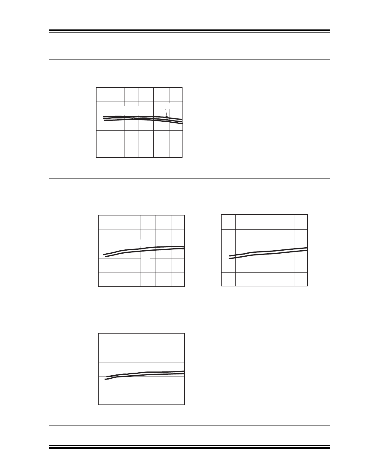
5. OUTPUT VOLTAGE vs. AMBIENT TEMPERATURE
V
IN
= -6.0V
V
IN
= -6.0V
2001-2012 Microchip Technology Inc.
DS21438C-page 9
TC59
5.0
TYPICAL CHARACTERISTICS (CONTINUED)
TC593002 (-3.0V)
AMBIENT TEMP. T
OPR
(
°
C
)
OUTPUT VOLTAGE V
OUT
(V)
V
IN
= -6.0V
-40
-20
0
20
40
60
-3.10
-3.05
-3.00
-2.95
-2.90
-2.85
80
I
OUT
= 1mA
40mA
5. OUTPUT VOLTAGE vs. AMBIENT TEMPERATURE (CONTINUED)
20mA
SUPPLY CURRENT I
SS
(
µ
A)
AMBIENT TEMP. T
OPR
(
°
C)
SUPPLY CURRENT I
SS
(
µ
A)
AMBIENT TEMP. T
OPR
(
°
C)
SUPPLY CURRENT I
SS
(
µ
A)
AMBIENT TEMP. T
OPR
(
°
C)
-40
-20
0
20
40
60
5
4
3
2
1
0
80
-40
-20
0
20
40
60
5
4
3
2
1
0
TC593002 (-3.0V)
80
-40
-20
0
20
40
60
5
4
3
2
1
0
TC594002 (-4.0V)
80
V
IN
= -10V
-6V
V
IN
= -10V
-5V
TC595002 (-5.0V)
V
IN
= -10V
-4V
6. SUPPLY CURRENT vs. AMBIENT TEMPERATURE
TC59
DS21438C-page 10
2001-2012 Microchip Technology Inc.
5.0
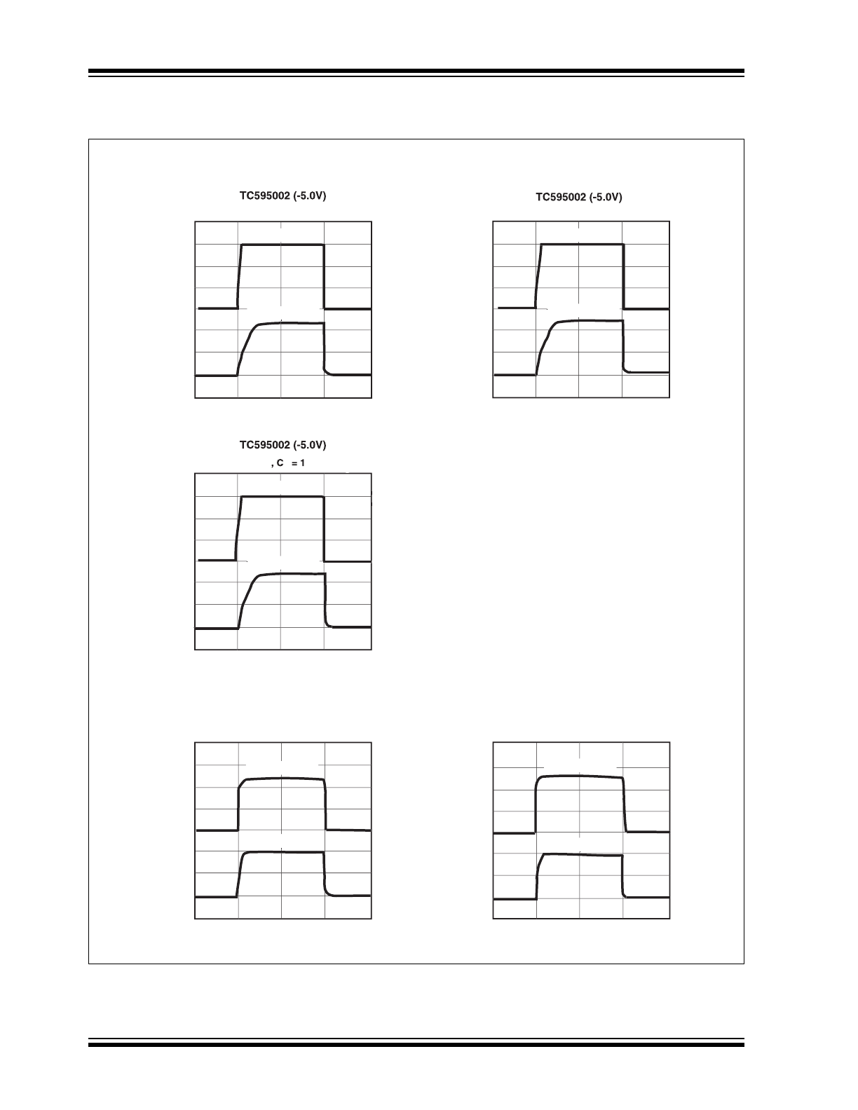
TYPICAL CHARACTERISTICS (CONTINUED)
INPUT VOLTAGE V
IN
(V)
TIME (2 msec/div)
INP
U
T V
O
LTA
G
E
V
IN
(V
)
INPUT VOLTAGE V
IN
(V)
OU
TP
U
T V
O
LTA
G
E
V
OU
T
(V
)
OU
TP
U
T V
O
LTA
G
E
V
OUT
(V
)
TIME (2 msec/div)
INPUT VOLTAGE V
IN
(V)
TIME (2 msec/div)
0
-2
-4
-6
OU
TP
U
T V
O
LTA
G
E
V
OU
T
(V
)
0
-2
-4
-6
OU
TP
U
T V
O
LTA
G
E
V
OU
T
(V
)
0
-2
-4
-6
OU
TP
U
T V
O
LTA
G
E
V
OUT
(V
)
0
-2
-4
0
-2
-4
0
-4
-8
TC594002 (-4.0V)
0
-4
-8
INP
U
T V
O
LTA
G
E
V
IN
(V
)
TC594002 (-4.0V)
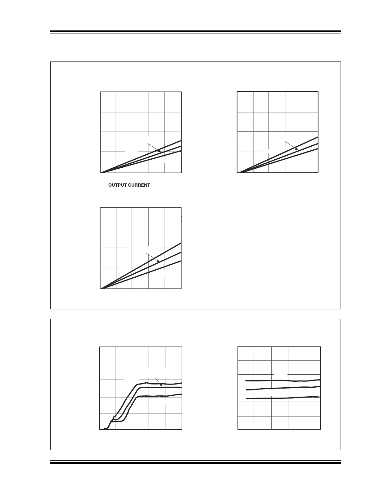
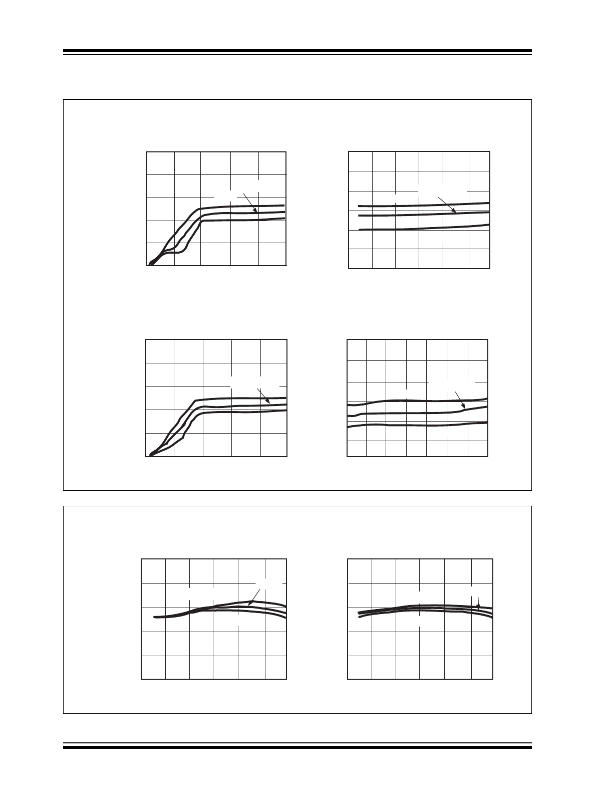
7. INPUT TRANSIENT RESPONSE
-2
-4
-6
-8
-6
-2
-6
-2
0
TIME (2 msec/div)
TIME (2 msec/div)
0
-6
-8
-4
-2
0
-6
-8
-4
-2
Input Voltage
Output Voltage
Output Voltage
Input Voltage
Input Voltage
Input Voltage
Input Voltage
Output Voltage
O
Output Voltage
Output Voltage
O
Output Voltage
Output Voltage
Output Voltage
Output Voltage
Output Voltage
I
OUT
= 1mA, C
IN
, C
L
= 1
µ
F, T
OPR
= 25
°
C
I
OUT
= 50mA, C
IN
, C
L
= 1
µ
F, T
OPR
= 25
°
C
I
OUT
= 100mA, C
IN
L
µ
F, T
OPR
= 25
°
C
I
OUT
= 1mA, C
IN
, C
L
= 1
µ
F, T
OPR
= 25
°
C
I
OUT
= 50mA, C
IN
, C
L
= 1
µ
F, T
OPR
= 25
°
C