
2001-2012 Microchip Technology Inc.
DS21437C-page 1
TC57
Features
• Low Dropout Voltage: 100mV @ 650mA with
FZT749 PNP Transistor
• 2.7V to 8V Supply Range
• Low Operating Current: 50
A Operating,
0.2
A Shutdown
• Low True Chip Enable
• Output Accuracy < ±2%
• Small Package: 5-Pin SOT-23A
Applications
• Battery Operated Systems
• Portable Instruments
• High-Efficiency Linear Regulator
• Post-Regulator for SMPS
• Power Supply or Battery Back-Up Supply for
Memory
Device Selection Table
Other output voltages and package options are available.
Please contact Microchip Technology Inc. for details.
Package Type
General Description
The TC57 is a low dropout regulator controller that
operates with an external PNP pass transistor, allowing
the user to tailor the LDO characteristics to suit the
application at hand. This results in lower dropout
operation (and often lower cost) compared with
traditional linear regulators with on-board pass
transistors. The maximum output current of a TC57-
based regulator circuit is limited only by the
characteristics of the external pass transistor. For
example, a maximum output current of 650mA (with a
dropout voltage of 100mV) results when an FZT749
pass transistor is used, while a Darlington configuration
can deliver up to 4A.
Flexibility, and superior performance make this family
of regulator controllers the ideal choice in applications
where low dropout voltage and low installed cost are
key.
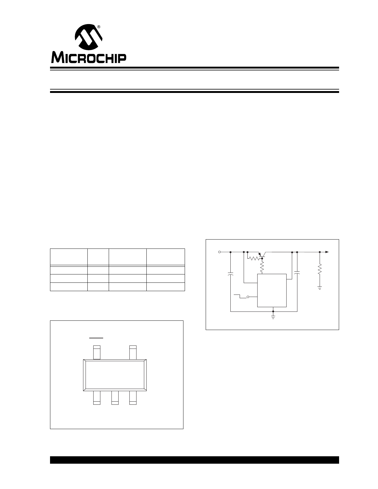
Functional Block Diagram
Part Number
Output
Voltage
Package
Temperature
Range
TC572502ECT
2.5V
5-Pin SOT-23A -40°C to +85°C
TC573002ECT
3.0V
5-Pin SOT-23A -40°C to +85°C
TC573302ECT
3.3V
5-Pin SOT-23A -40°C to +85°C
SHDN
5
5-Pin SOT-23A
TC57
1
3
4
EXT
2
V
IN
V
OUT
GND
NOTE: 5-Pin SOT-23A is equivalent to the EIAJ SC-74A.
TC573002ECT
V
OUT
GND
SHDN
V
IN
EXT
C
IN
10μF
(Tantalum)
FZT749
Q1
R
B
1K
C
L
10
μF
(Tantalum)
R
L
V
IN
+3.3V
R
BE
47K
1
2
ON
OFF
3
4
5
V
OUT
+3V
3.3V Line Input, 3.0V, 500mA Output LDO
Line Regulator Controller
TC57
DS21437C-page 2
2001-2012 Microchip Technology Inc.
1.0
ELECTRICAL
CHARACTERISTICS
Absolute Maximum Ratings*
Input Voltage ........................................................+12V
Output Current ....................................................50mA
Output Voltage............................. -0.3V to (V
IN
+ 0.3V)
Power Dissipation.............................................150mW
Operating Temperature Range............. -40°C to +85°C
Storage Temperature Range ..............-40°C to +150°C
*Stresses above those listed under "Absolute Maximum
Ratings" may cause permanent damage to the device. These
are stress ratings only and functional operation of the device
at these or any other conditions above those indicated in the
operation sections of the specifications is not implied.
Exposure to Absolute Maximum Rating conditions for
extended periods may affect device reliability.
TC55 ELECTRICAL SPECIFICATIONS
TC57EP3002 Electrical Characteristics: SHDN = GND, V
IN
= V
OUT
+ 1V, V
OUT
= 3V to 5V, I
OUT
= 0, T
A
= 25°C, Test Circuit of
Figure 3-1, unless otherwise noted. (Note 2)
Symbol
Parameter
Min
Typ
Max
Units
Test Conditions
V
IN
Input Voltage
—
—
8
V
V
EXT
Voltage on EXT Output
—
—
8
V
V
OUT
Output Voltage
0.98
X
V
R
V
R
±0.5% 1.02
X
V
R
V
I
OUT
= 50mA (Note 1)
V
OUT
Load Regulation
-60
—
60
mV
1mA
I
OUT
100mA (Note 3)
V
IN
- V
OUT
Dropout Voltage
—
100
—
mV
I
OUT
= 100mA (Note 2)
I
DD
Supply Current
—
50
80
A
V
SHDN
= V
IN
= 5V
I
SHDN
Shutdown Supply Current
—
—
0.6
A
V
SHDN
= GND
V
OUT
/
V
IN
Line Regulation
—
0.1
0.3
%/V
I
OUT
= 50mA, 4V
V
IN
8V
(Note 3)
V
OUT
/
T
V
OUT
Temperature Coefficient
—
±100
—
ppm/°C
I
OUT
= 10mA, -40°C <
T
J
85°C
(Note 3)
I
LEXT
EXT Pin Leakage Current
—
—
0.5
A
I
EXT
EXT Sink Current
—
—
25
mA
Note 4
V
IH
SHDN Input High Logic Threshold
1.5
—
—
V
V
IL
SHDN Input Low Logic Threshold
—
—
0.25
V
I
IH
SHDN Input Current @ V
IH
—
—
0.1
A
V
SHDN
= V
IN
= 5V
I
IL
SHDN Input Current @ V
IL
-0.2
-0.05
0
A
V
SHDN
= GND
Note
1:
V
R
is the regulator output voltage setting.
2:
Dropout voltage is defined as the input to output differential at which the output voltage drops 2% below its nominal value measured at a
1V differential.
3:
Varies with type of pass transistor used. Numbers shown are for the test circuit of Figure 3-1.
4:
The product of I
EXT
X
V
EXT
must be less than the maximum allowable power dissipation.
2001-2012 Microchip Technology Inc.
DS21437C-page 3
TC57
2.0
PIN DESCRIPTIONS
The descriptions of the pins are listed in Table 2-1.
TABLE 2-1:
PIN FUNCTION TABLE
Pin No.
(5-Pin SOT-23A)
Symbol
Description
1
GND
Ground terminal.
2
V
IN
Supply voltage input. Positive input voltage of 2.7V to 8.0V.
3
V
OUT
Regulator voltage sense input. Connects to the collector of the external PNP pass transistor.
4
EXT
Base Drive for the external PNP pass transistor.
5
SHDN
Shutdown Input. The device is enabled when SHDN
V
IL
. The device enters a low power
shutdown state when SHDN
V
IH
. During shutdown, the output is disabled, and supply current
falls to less than 1
A.
TC57
DS21437C-page 4
2001-2012 Microchip Technology Inc.
3.0
DETAILED DESCRIPTION
The TC57 series of precision low dropout regulator
controllers use an external PNP transistor to
accommodate a wide range of output currents. A series
resistor (R
B
) limits the maximum base current drawn
from the PNP transistor. Limiting the base drive both
determines the regulator’s output current capability, as
well as limits ground current when the device is
operated in dropout. The PNP transistor’s V
CE(SAT)
is
the only factor limiting dropout voltage.
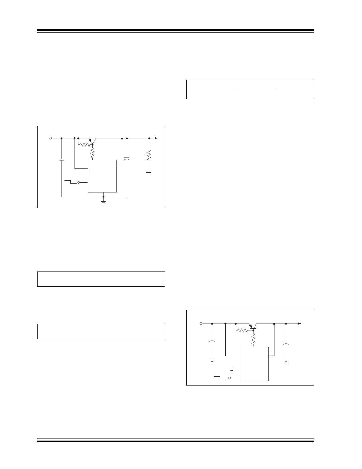
FIGURE 3-1:
TEST CIRCUIT
3.1
Transistor Selection
The PNP pass transistor must have satisfactory power
dissipation, current gain, and collector current specifi-
cations to suit the application at hand. The maximum
output current the circuit can deliver is influenced by
h
FE
. The highest guaranteed output current is given by:
EQUATION 3-1:
The transistor’s actual power dissipation (PD) is equal
to the maximum load current times the maximum input/
output voltage differential, or:
EQUATION 3-2:
The ideal transistor has a minimum h
FE
of 100, and a
V
CE(SAT)
of less than 0.6V at full output current. For
example, the Zetex FZT749 has an h
FE
of 170 at a
collector current of 1A, and a guaranteed V
CE(SAT)
of
0.3V at a base current of 100mA. It is packaged in a
SOT-223 and is recommended for use with the TC57.
Other transistors are also suitable, depending on the
required input and output voltages and output current
(Table 3-1).
3.2
Base-Current Limiting Resistor
Base current limiting resistor R
B
can be estimated
using:
EQUATION 3-3:
Where:
h
FE
is the current gain of the pass transistor
V
IN
I
s the input voltage (in volts)
V
BE
is the base-emitter voltage at the desired
output current (in volts)
I
OUT
is the output current (in Amps)
For example, assume a desired continuous output
current of 1.0A, an input voltage of 5V, and an FZT749
pass transistor. The FZT749 has a typical h
FE
of 170,
and a V
BE
of 0.8V; both specified at a collector current
of 1.0A. Substituting these values into the equation
above results in an R
B
value of 704
(closest standard
value = 680
).
3.3
Pull-Up Resistor and Output
Capacitor
A pull-up resistor (R
BE
, installed between the base and
emitter of the pass transistor) facilitates rapid turn-off of
the pass transistor in the event of a sudden decrease in
load (Figure 3-2). Recommended values for this
resistor are between 20K
and 47K. A Tantalum
output capacitor of at least 10
F must be used to
guarantee stability. Higher values decrease output
noise and eliminate power-on overshoot, but extend
power-up times. Table 3-1 lists several capacitor
choices.
FIGURE 3-2:
3.3V, 1A REGULATOR
USING 5V SUPPLY INPUT
TC573002ECT
V
OUT
GND
SHDN
VIN
EXT
C
IN
10μF
(Tantalum)
FZT749
Q1
R
B
680
Ω
C
L
10
μF
(Tantalum)
R
L
V
IN
R
BE
33K
1
2
ON
OFF
3
4
5
V
OUT
I
LOAD(MAX)
= 25 mA x h
FE(MIN)
P
D
I
LOAD(MAX)
x (V
IN(MAX)
– V
OUT(MIN)
)
h
FE
(V
IN
– V
BE
)
I
OUT
R
B
=
TC57
V
OUT
SHDN
V
IN
EXT
C
IN
10μF
(Tantalum)
FZT749
Q1
R
B
680
Ω
C
OUT
10
μF
(Tantalum)
V
IN
= 5V
R
BE
33K
Ω
1
2
ON
OFF
3
4
5
V
OUT
= 3.3V
GND
2001-2012 Microchip Technology Inc.
DS21437C-page 5
TC57
3.4
Input Capacitor
The addition of an input capacitor further reduces
output noise, and negates the effects of power supply
input impedance. A 10
F (min) Tantalum capacitor is
recommended.
3.5
Shutdown Mode
The TC57 enters a low power shutdown mode when
the shutdown input (SHDN) is high. During shutdown,
the regulator is disabled, the output capacitor is
discharged through the load, and supply current to the
TC57 decreases to less than 1
A. Normal operation
resumes when SHDN is brought low. If the shutdown
mode is not used, SHDN should be tied to V
IN
.
TABLE 3-1:
COMPONENT SUPPLIERS
Device
Mounting
Method
Manufacturer
Website
CAPACITORS
267 Series
Surface Mount
Matsuo
http://www.matsuoelectronics.com
F95 Tantalum Series
Surface Mount
Nichicon
http://www.nichicon-us.com
595 Tantalum Series
Surface Mount
Sprague
http://www.vishay.com/brands/sprague
OS-CON Series
Through-Hole
Sanyo
http://www.sanyovideo.com
LXF Series
Through-Hole
United Chemi-Con
http://chemi-con.com
TRANSISTORS
ZTX749
Through-Hole
Zetex
http://www.zetex.com
2N4403
Through-Hole
ON SEMI
http://www.onsemi.com/home
2N2907A
Through-Hole
ON SEMI
http://www.onsemi.com/home
FZT749
Surface Mount
Zetex
http://www.zetex.com
TC57
DS21437C-page 6
2001-2012 Microchip Technology Inc.
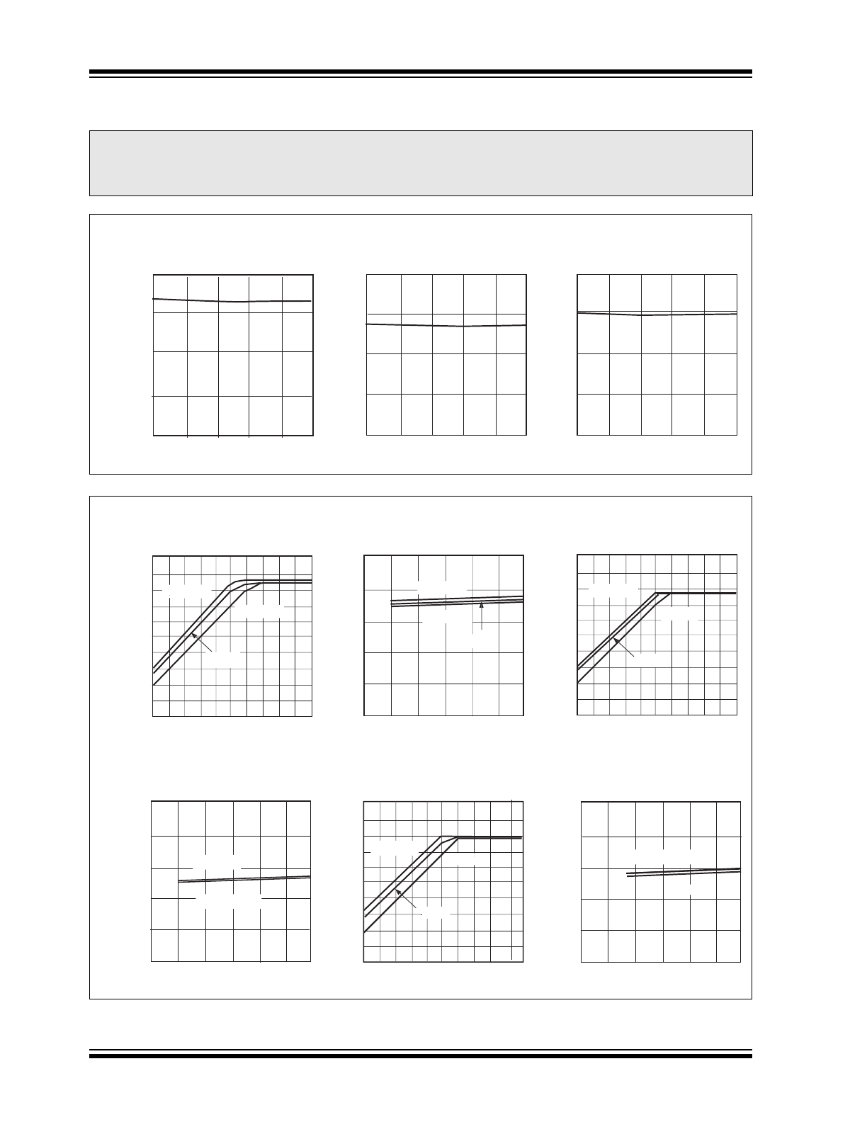
4.0
TYPICAL CHARACTERISTICS
Note:
The graphs and tables provided following this note are a statistical summary based on a limited number of
samples and are provided for informational purposes only. The performance characteristics listed herein are
not tested or guaranteed. In some graphs or tables, the data presented may be outside the specified
operating range (e.g., outside specified power supply range) and therefore outside the warranted range.
5.1
5.0
4.8
4.7
0
100
200
300
400
500
4.9
TC575002 (5V)
1. OUTPUT VOLTAGE vs. OUTPUT CURRENT
OUTPUT VOLTAGE V
OUT
(V)
OUTPUT VOLTAGE V
OUT
(V)
OUTPUT VOLTAGE V
OUT
(V)
4.1
4.0
3.8
3.7
0
100
200
300
400
500
OUTPUT CURRENT I
OUT
(mA)
OUTPUT CURRENT I
OUT
(mA)
OUTPUT CURRENT I
OUT
(mA)
3.9
TC574002 (4V)
3.4
3.3
3.1
3.0
0
100
200
300
400
500
3.2
TC573302 (3.3V)
T
A
= 25
°C
V
IN
= 6V, C
L
= 10
μF (Tantalum)
T
A
= 25
°C
V
IN
= 5V, C
L
= 10
μF (Tantalum)
T
A
= 25
°C
V
IN
= 4.3V, C
L
= 10
μF (Tantalum)
2. OUTPUT VOLTAGE vs. INPUT VOLTAGE
4.2
4.0
3.6
3.4
4.0
4.5
3.2
3.5
INPUT VOLTAGE V
IN
(V)
INPUT VOLTAGE V
IN
(V)
3.8
OUTPUT VOLTAGE V
OUT
(V)
OUTPUT VOLTAGE V
OUT
(V)
4.10
4.05
3.95
3.90
3.85
4
5
6
7
8
4.00
TC574002 (4V)
TC574002 (4V)
5.2
5.0
4.6
4.4
5.0
5.5
4.2
4.5
INPUT VOLTAGE V
IN
(V)
4.8
C
L
= 10
μF (Tantalum), T
A
= 25
°C
OUTPUT VOLTAGE V
OUT
(V)
TC575002 (5V)
3.5
3.3
2.9
2.7
3.3
3.8
2.5
2.8
INPUT VOLTAGE V
IN
(V)
3.1
OUTPUT VOLTAGE V
OUT
(V)
TC573302 (3.3V)
INPUT VOLTAGE V
IN
(V)
OUTPUT VOLTAGE V
OUT
(V)
5.10
5.05
4.95
4.90
4.85
5
6
7
5.00
TC575002 (5V)
6
INPUT VOLTAGE V
IN
(V)
OUTPUT VOLTAGE V
OUT
(V)
3.40
3.35
3.25
3.20
3.15
3
4
5
3.30
TC573302 (3.3V)
I
OUT
= 1mA
100mA
500mA
100mA
500mA
100mA, 500mA
I
OUT
= 1mA, 100mA
I
OUT
= 1mA
I
OUT
= 1mA
I
OUT
= 1mA
500mA
I
OUT
A
A
= 1mA
500mA
100mA
1
1
100mA
5
500mA
C
L
= 10
μF (Tantalum), T
A
= 25
°C
C
L
= 10
μF (Tantalum), T
A
= 25
°C
C
L
= 10
μF (Tantalum), T
A
= 25
°C
C
L
= 10
μF (Tantalum), T
A
= 25
°C
C
L
= 10
μF (Tantalum), T
A
= 25
°C
2001-2012 Microchip Technology Inc.
DS21437C-page 7
TC57
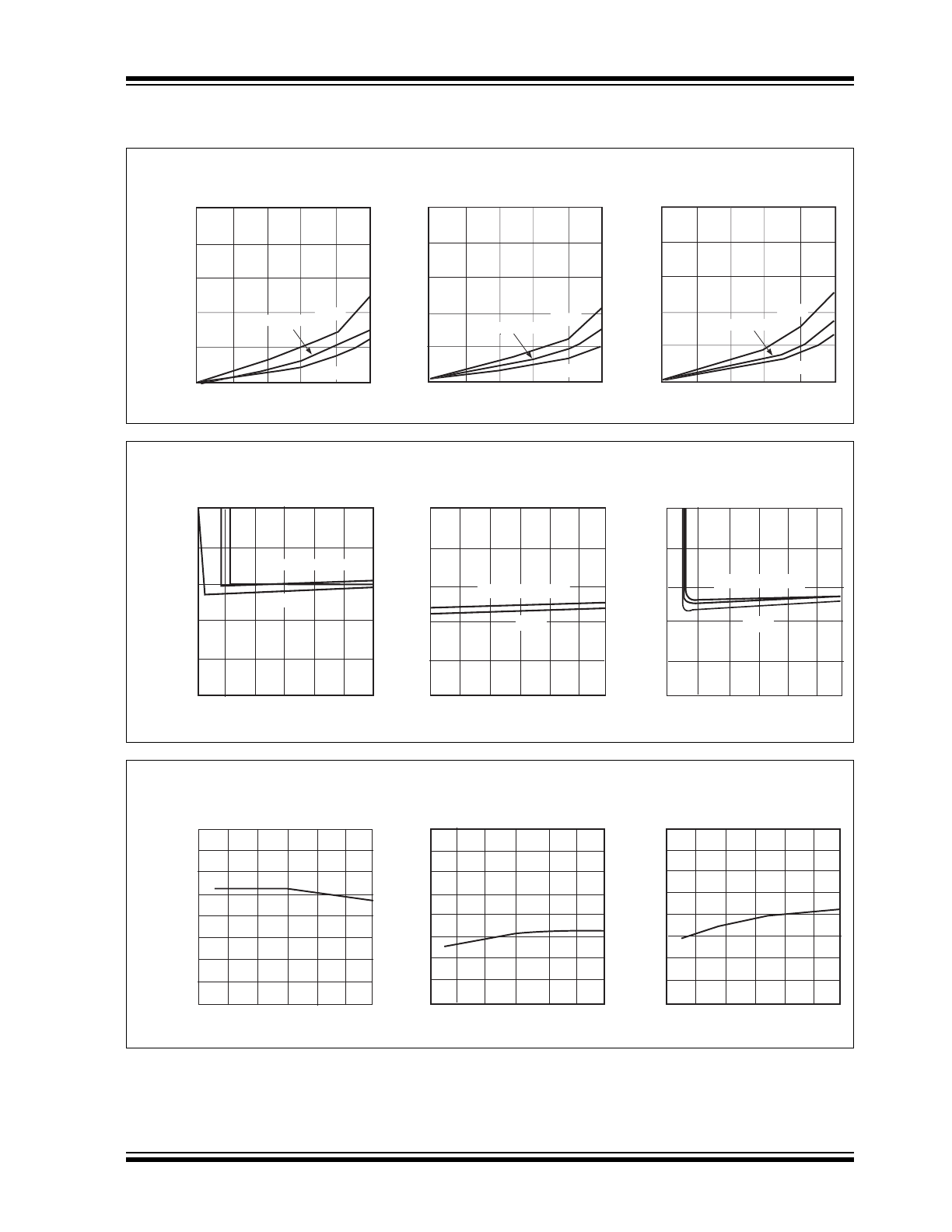
4.0
TYPICAL CHARACTERISTICS (CONTINUED)
0.8
1.0
0.6
0.2
0.0
0
200
400
600
800
1000
0.4
TC575002 (5V)
C
L
= 10
μF (Tantalum)
3. DROPOUT VOLTAGE vs. OUTPUT CURRENT
DROPOUT VOLTAGE V
IN
-V
OUT
DROPOUT VOLTAGE V
IN
-V
OUT
DROPOUT VOLTAGE V
IN
-V
OUT
0.8
1.0
0.6
0.2
0.0
0
200
400
600
800
1000
OUTPUT CURRENT I
OUT
(mA)
OUTPUT CURRENT I
OUT
(mA)
OUTPUT CURRENT I
OUT
(mA)
0.4
TC574002 (4V)
1.0
0.8
0.4
0.2
0.0
0
200
400
600
800
1000
0.6
TC573302 (3.3V)
-3
30
°C
-30
0
°C
-30
°C
80
°C
80
°C
80
°C
T
OPR
= 25
°C
C
L
= 10
μF (Tantalum)
C
L
= 10
μF (Tantalum)
T
OPR
R
OPR
= 25
°C
T
T
OPR
25
= 25
°°°C
C
4. SUPPLY CURRENT vs. INPUT VOLTAGE
50
40
20
10
4
6
5
0
3
INPUT VOLTAGE V
IN
(V)
30
SUPPLY CURRENT I
DD
(μ
A)
7
TC573302 (3.3V)
50
40
20
10
6
7
8
0
5
INPUT VOLTAGE V
IN
(V)
30
SUPPLY CURRENT I
DD
(μ
A)
TC575002 (5V)
INPUT VOLTAGE V
IN
(V)
SUPPLY CURRENT I
DD
(μ
A)
50
40
20
10
0
4
5
6
30
TC574002 (4V)
-30
°C
-30
°C
-30
°C
T
OPR
= 25
°C, 80°C
T
OPR
= 25
°C, 80°C
T
OPR
= 25
°C, 80°C
5. OUTPUT VOLTAGE vs. AMBIENT TEMPERATURE
AMBIENT TEMP.
TA
(
°
C)
V
IN
= 6.0V
I
OUT
= 100mA, C
L
= 10
μF (Tantalum)
OUTPUT VOLTAGE V
OUT
(V)
5.10
5.05
4.95
4.90
-40
-20
0
20
40
60
80
5.00
TC575002 (5V)
4.10
4.05
3.95
3.90
20
40
60
80
-40
-20
0
AMBIENT TEMP.
TA
(
°
C)
4.00
OUTPUT VOLTAGE V
OUT
(V)
TC574002 (4V)
80
AMBIENT TEMP.
TA
(
°
C)
OUTPUT VOLTAGE V
OUT
(V)
3.40
3.35
3.25
3.20
-40
-20
0
20
40
60
3.30
TC573302 (3.3V)
V
IN
= 5.0V
I
OUT
= 100mA, C
L
= 10
μF (Tantalum)
V
IN
= 4.3V
I
OUT
= 100mA, C
L
= 10
μF (Tantalum)
TC57
DS21437C-page 8
2001-2012 Microchip Technology Inc.
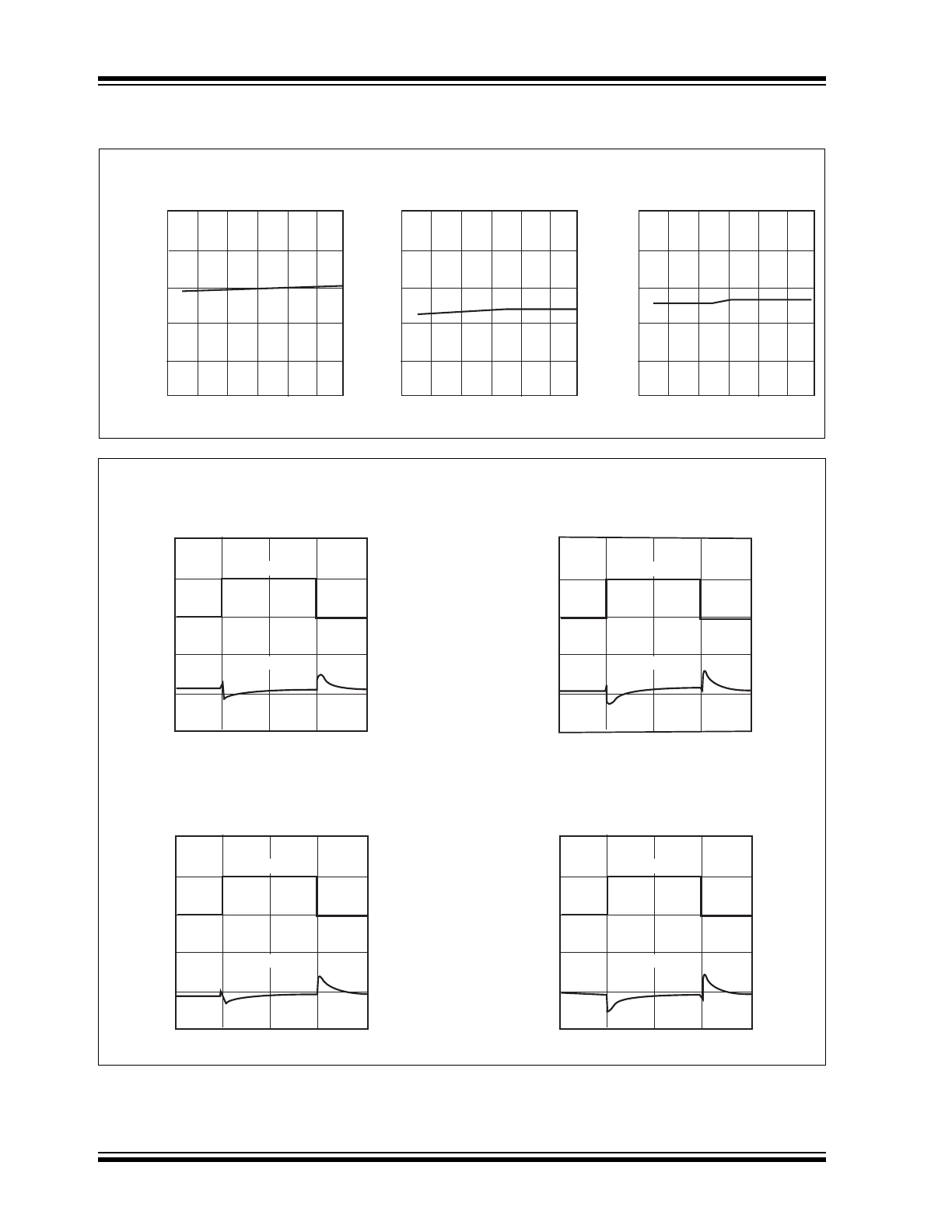
4.0
TYPICAL CHARACTERISTICS (CONTINUED)
40
50
30
10
0
-20
-40
0
20
40
60
80
-20
-40
0
20
40
60
80
-20
-40
0
20
40
60
80
20
TC575002 (5V)
V
IN
= 6V
6. SUPPLY CURRENT vs. AMBIENT TEMPERATURE
SUPPLY CURRENT I
DD
(μ
A)
SUPPLY CURRENT I
DD
(μ
A)
SUPPLY CURRENT I
DD
(μ
A)
40
50
30
10
0
AMBIENT TEMP. T
A
(
°
C)
AMBIENT TEMP. T
A
(
°
C)
AMBIENT TEMP. T
A
(
°
C)
20
TC574002 (4V)
50
40
20
10
0
30
TC573302 (3.3V)
V
IN
= 5V
V
IN
= 4.3V
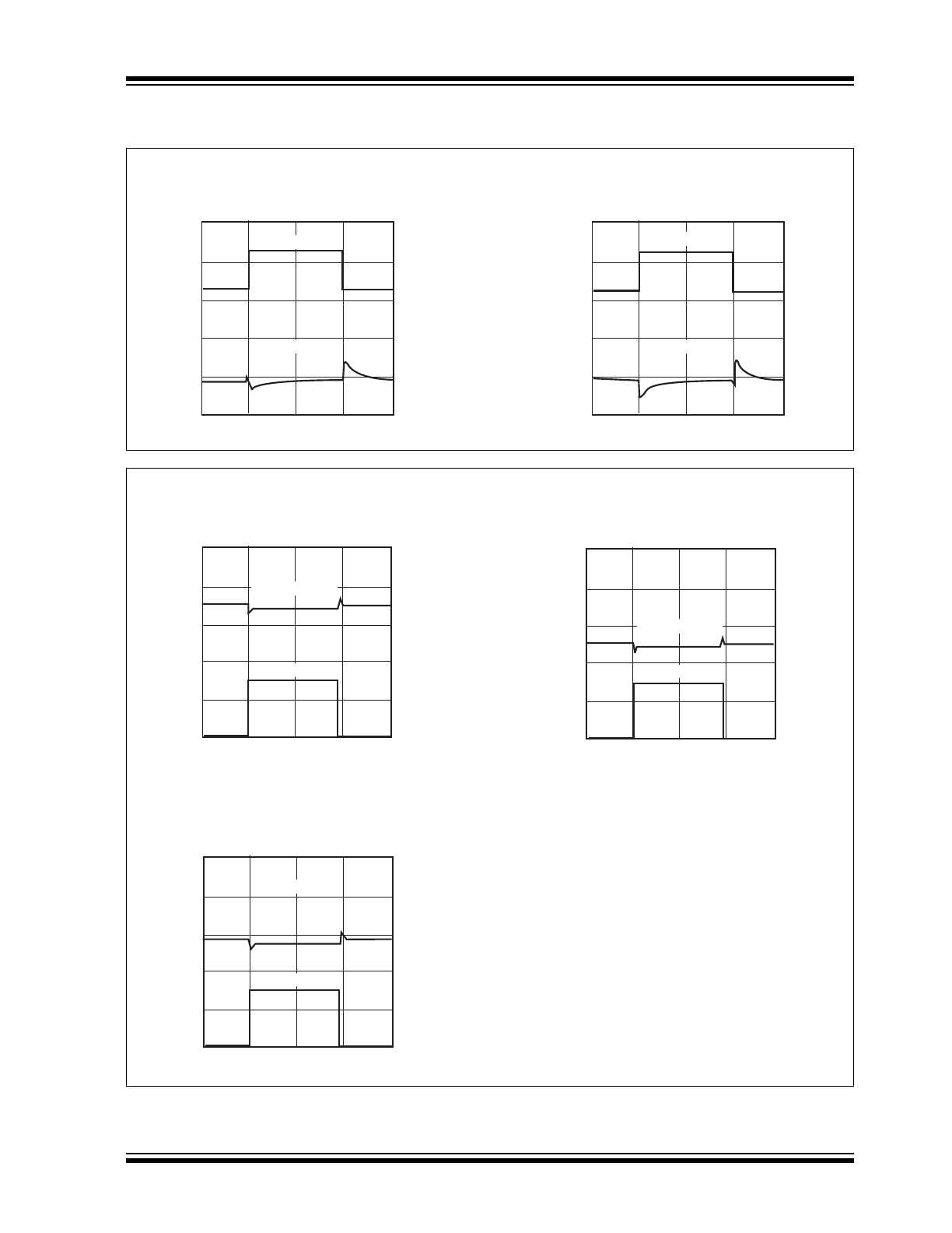
7. INPUT TRANSIENT RESPONSE
5.4
5.3
5.1
5.0
4.9
Time (0.4 msec/div)
5.2
8
7
5
4
3
6
INPUT VOLTAGE V
IN
(V)
OUTPUT VOLTAGE V
OUT
(V)
TC575002 (5V)
I
OUT
= 10mA, C
L
= 10
μF (Tantalum)
Input Voltage
Output Voltage
5.4
5.3
5.1
5.0
4.9
Time (0.4 msec/div)
5.2
8
7
5
4
3
6
INPUT VOLTAGE V
IN
(V)
OUTPUT VOLTAGE V
OUT
(V)
TC575002 (5V)
4.4
4.3
4.1
4.0
3.9
Time (0.4 msec/div)
4.2
4.4
4.3
4.1
4.0
3.9
4.2
7
6
4
3
2
5
7
6
4
3
2
5
INPUT VOLTAGE V
IN
(V)
OUTPUT VOLTAGE V
OUT
(V)
TC574002 (4V)
Time (0.4 msec/div)
INPUT VOLTAGE V
IN
(V)
OUTPUT VOLTAGE V
OUT
(V)
TC574002 (4V)
Input Voltage
Output Voltage
Input Voltage
Output Voltage
Input Voltage
Output Voltage
I
OUT
= 10mA, C
L
= 10
μF (Tantalum)
I
OUT
= 100mA, C
L
= 10
μF (Tantalum)
I
OUT
= 100mA, C
L
= 10
μF (Tantalum)
2001-2012 Microchip Technology Inc.
DS21437C-page 9
TC57
4.0
TYPICAL CHARACTERISTICS (CONTINUED)
7. INPUT TRANSIENT RESPONSE (CONT.)
Time (0.4 msec/div)
3.7
3.6
3.4
3.3
3.2
3.5
3.7
3.6
3.4
3.3
3.2
3.5
6
5
3
2
1
4
6
5
3
2
1
4
INPUT VOLTAGE V
IN
(V)
OUTPUT VOLTAGE V
OUT
(V)
TC573302 (3.3V)
Input Voltage
Output Voltage
Time (0.4 msec/div)
INPUT VOLTAGE V
IN
(V)
OUTPUT VOLTAGE V
OUT
(V)
TC573302 (3.3V)
I
OUT
= 100mA, C
L
= 10
μF (Tantalum)
I
OUT
= 10mA, C
L
= 10
μF (Tantalum)
Input Voltage
Output Voltage
8. LOAD TRANSIENT RESPONSE
1000
800
400
200
300mA
1mA
1mA
1mA
300mA
300mA
0
Time (10 msec/div)
600
OUTPUT VOLTAGE V
OUT
(V)
OUTPUT CURRENT I
OUT
(mA)
TC575002 (5V)
1000
800
400
200
0
600
1000
800
400
200
0
600
V
IN
= 6V, C
L
= 10
μF (Tantalum)
Output Voltage
Output Current
Time (10 msec/div)
4.10
4.05
3.95
3.90
3.85
4.00
5.10
5.05
4.95
4.90
4.85
5.00
3.40
3.35
3.25
3.20
3.15
3.30
OUTPUT VOLTAGE V
OUT
(V)
OUTPUT CURRENT I
OUT
(mA)
TC574002 (4V)
Time (10 msec/div)
OUTPUT VOLTAGE V
OUT
(V)
OUTPUT CURRENT I
OUT
(mA)
TC573302 (3.3V)
Output Voltage
Output Current
Output Voltage
Output Current
V
IN
= 5V, C
L
= 10
μF (Tantalum)
V
IN
= 4.3V, C
L
= 10
μF (Tantalum)
TC57
DS21437C-page 10
2001-2012 Microchip Technology Inc.
5.0
PACKAGING INFORMATION
5.1
Package Marking Information
5.2
Taping Form
Symbol
Voltage
2
2.
3
3.
4
4.
5
5.
6
6.
3
1
represents integer part of output voltage
Symbol
Voltage
Symbol
Voltage
0
.0
5
.5
1
.1
6
.6
2
.2
7
.7
3
.3
8
.8
4
.4
9
.9
2
represents first decimal of output voltage
3
represents production lot ID code
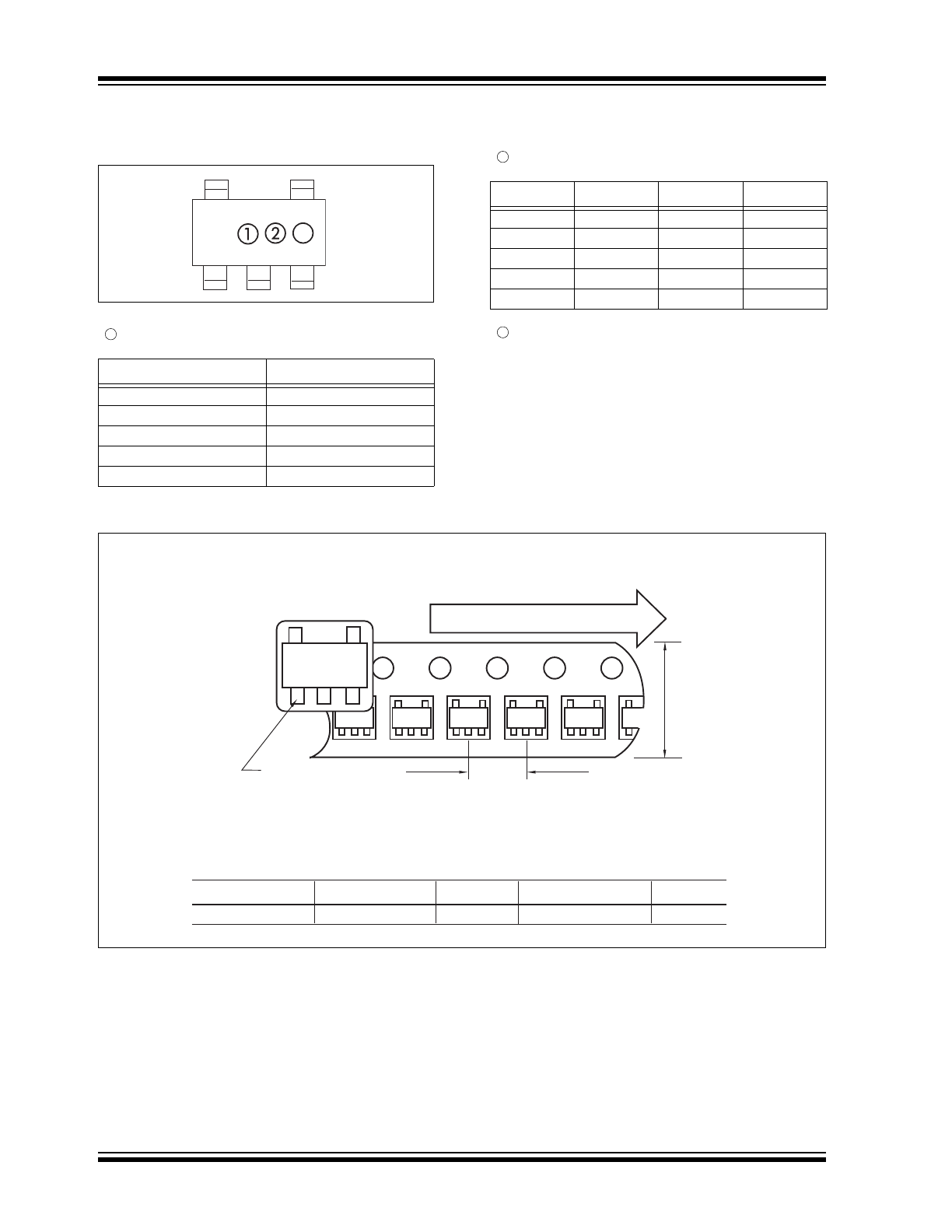
Component Taping Orientation for 5-Pin SOT-23A (EIAJ SC-74A) Devices
Package
Carrier Width (W)
Pitch (P)
Part Per Full Reel
Reel Size
5-Pin SOT-23A
8 mm
4 mm
3000
7 in
Carrier Tape, Number of Components Per Reel and Reel Size
User Direction of Feed
Device
Marking
PIN 1
Standard Reel Component Orientation
TR Suffix Device
(Mark Right Side Up)
W
P