
© 2007 Microchip Technology Inc.
DS21433C-page 1
TC530/TC534
Features
• Precision (up to 17-Bits) A/D Converter
• 3-Wire Serial Port
• Flexible: User Can Trade Off Conversion Speed
For Resolution
• Single Supply Operation
• -5V Output Pin
• 4 Input, Differential Analog MUX (TC530)
• Automatic Input Polarity and Overrange Detection
• Low Operating Current: 5mA Max
• Wide Analog Input Range: ±4.2V Max
• Cost Effective
Applications
• Precision Analog Signal Processor
• Precision Sensor Interface
• High Accuracy DC Measurements
General Description
The TC530/TC534 are serial analog data acquisition
subsystems ideal for high precision measurements (up
to 17-bits plus sign). The TC534 consists of a dual
slope integrating A/D converter, negative power
supply generator and 3 wire serial interface port. The
TC530 is identical to the TC534, but adds a four
channel differential input multiplexer. Key A/D
converter operating parameters (Auto Zero and Inte-
gration time) are programmable, allowing the user to
trade conversion time for resolution.
Data conversion is initiated when the RESET input is
brought low. After conversion, data is loaded into the
output shift register and EOC is asserted, indicating
new data is available. The converted data (plus Over-
range and polarity bits) is held in the output shift
register until read by the processor or until the next
conversion is completed, allowing the user to access
data at any time.
The TC530/TC534 timebase can be derived from an
external crystal of 2MHz (max) or from an external fre-
quency source. The TC530/TC534 requires a single 5V
power supply and features a -5V, 10mA output which
can be used to supply negative bias to other
components in the system.
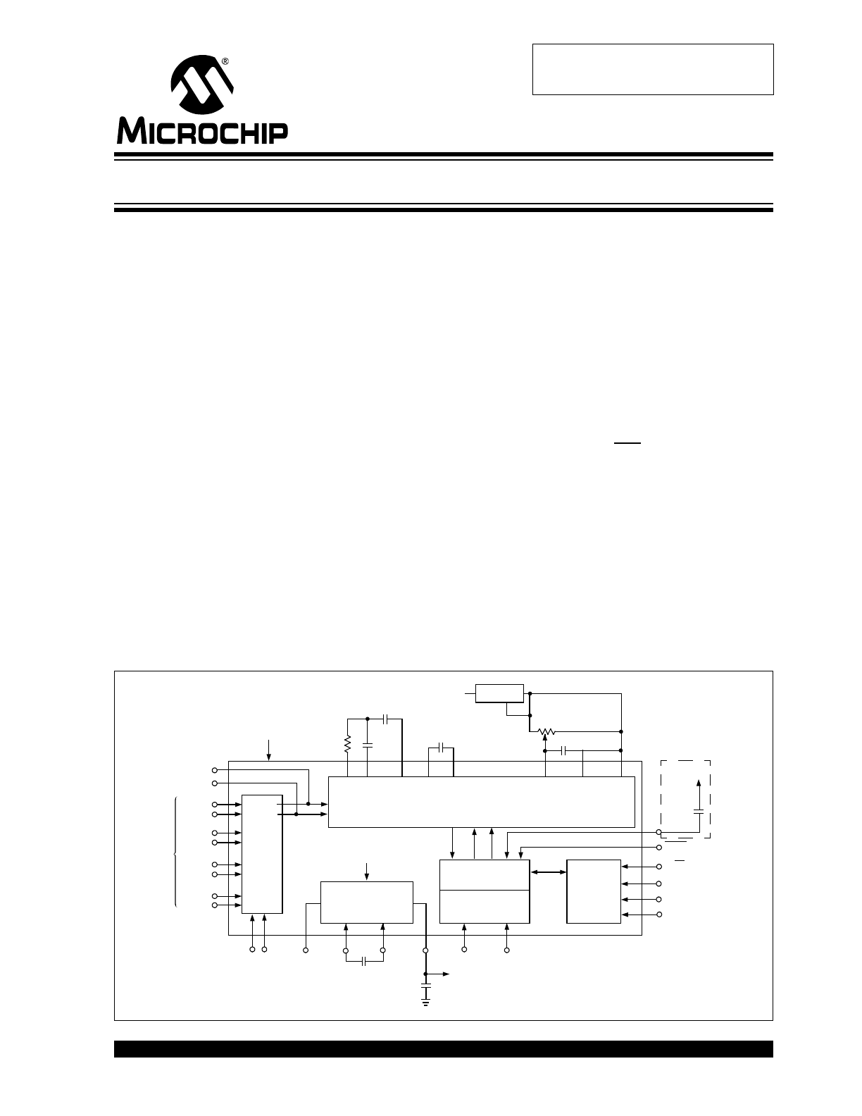
Typical Application
A0 A1
OSC
IN
R/W
D
IN
D
OUT
D
CLK
OSC
OUT
OSC
RESET
CAP+ CAP–
C
AZ
TC530
TC534
C
REF
R
INT
C
INT
TC534
(Only)
(TC530 Only)
DC-TO-DC
Converter
State
Machine
Serial Port
Negative
Supply Output
Oscillator
(
÷
4)
Dual Slope A/D Converter
.01 µF
0.01 µF
Optional
Power-On
Reset Cap
100 k
Ω
+5V
DIF.
MUX
(TC534
Only)
A
B
CMPTR
BUF
INT
C
AZ
ACOM
V
DD
V
DD
V
DD
V
DD
V
SS
MCP1525
V
REF-
V
REF+
V
IN-
V
IN+
EOC
CH2+
CH3+
CH1+
CH4+
CH4-
CH3-
CH2-
CH1-
IN+
IN-
C
REF-
C
REF+
5V Precision Data Acquisition Subsystems
Obsolete Device
TC530/TC534
DS21433C-page 2
© 2007 Microchip Technology Inc.
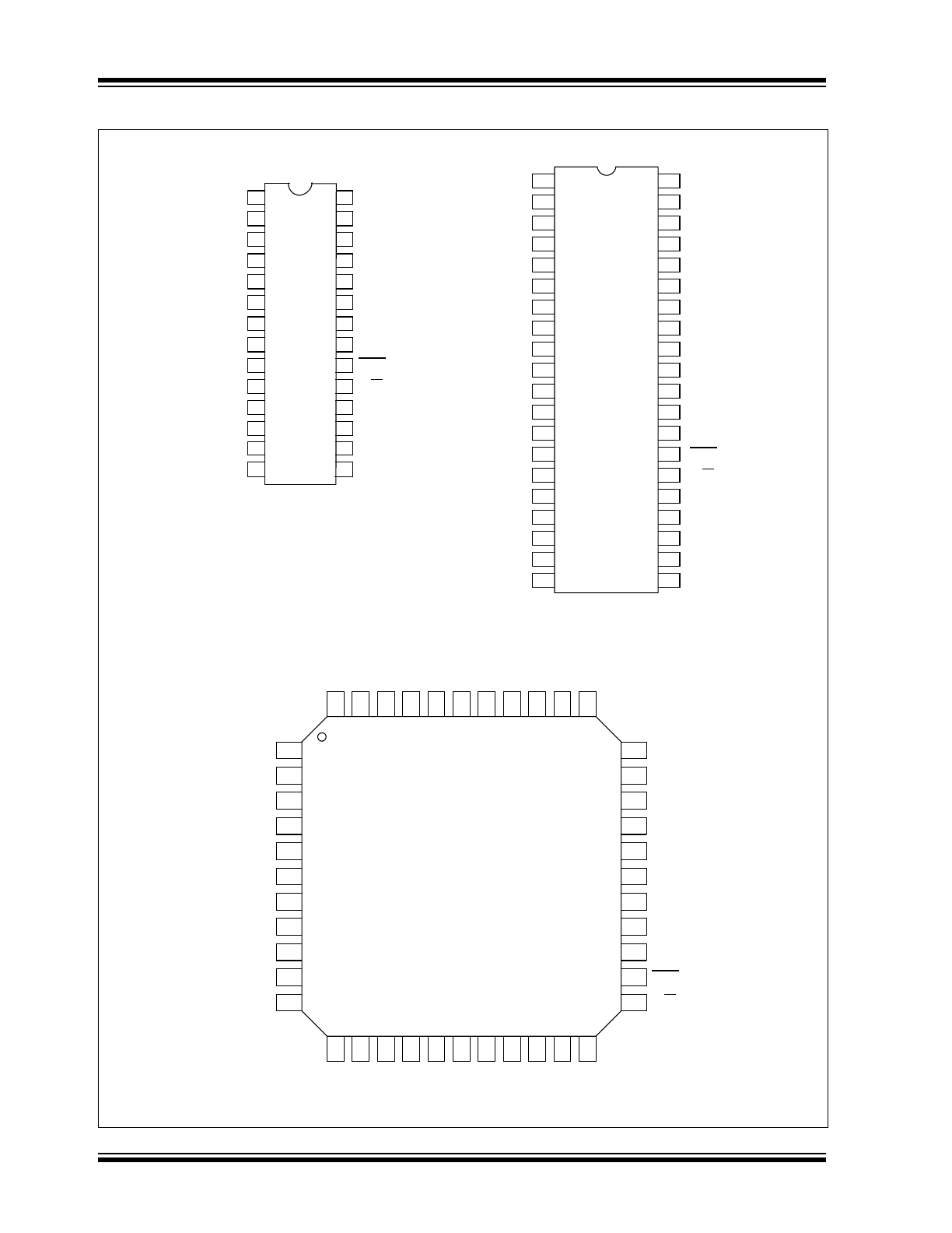
Package Types
1
2
3
4
20
19
18
5
6
7
8
17
23
22
21
9
10
11
12
24
25
26
27
28
TC530CPI
TC530COI
16
15
13
14
V
SS
C
REF-
C
REF+
V
REF-
V
REF+
C
INT
C
AZ
BUF
ACOM
OSC
OUT
V
IN-
V
IN+
DGND
N/C
V
CCD
V
DD
D
OUT
D
CLK
CAP-
AGND
RESET
N/C
OSC
CAP+
OSC
IN
D
IN
R/W
EOC
28-Pin SOIC
28-Pin PDIP
TC534CPL
1
2
3
4
5
6
7
8
9
10
11
12
13
14
15
16
17
18
19
20
40
39
38
37
36
35
34
33
32
31
30
29
28
27
26
25
24
23
22
21
40-Pin PDIP
V
CDD
V
DD
OS
C
OUT
CAP-
CAP+
OSC
IN
D
OUT
D
CL
K
D
IN
CH
2+
CH
3+
CH
1+
DG
N
D
AGND
A1
A0
27
26
25
24
23
7
8
9
10
11
N/C
N/C
12 13 14 15 16 17 18 19 20 21 22
38 37 36 35 34
N/
C
39
40
41
42
43
44
28
29
30
31
32
33
6
5
4
3
2
1
BUF
C
AZ
V
SS
C
IN
T
N/
C
N/
C
N/C
OSC
RESET
N/C
N/C
N/C
EOC
N/C
R/W
TC534CKW
44-Pin MQFP
CH4+
CH4-
CH3-
CH2-
CH1-
C
REF-
C
REF+
V
REF-
V
REF+
ACOM
V
SS
C
REF-
C
REF+
V
REF-
V
REF+
C
INT
C
AZ
BUF
ACOM
A0
CH4-
CH3-
DGND
A1
CH2-
CH1-
CH4+
CH3+
CH2+
CH1+
V
CCD
V
DD
D
OUT
D
CLK
CAP-
AGND
RESET
N/C
OSC
CAP+
OSC
IN
D
IN
R/W
EOC
OSC
OUT
N/C
N/C
N/C
N/C
N/C
© 2007 Microchip Technology Inc.
DS21433C-page 3
TC530/TC534
1.0
ELECTRICAL
CHARACTERISTICS
Absolute Maximum Ratings †
Supply Voltage ......................................................+6V
Analog Input Voltage (V
IN
+
or V
IN
-).............V
DD
to V
SS
Logic Input Voltage......... (V
DD
+ 0.3V) to (GND - 0.3V)
Ambient Operating Temperature Range:
PDIP Package (C) ............................... 0°C to +70°C
SOIC Package (C)............................... 0°C to +70°C
MQFP Package (C) ............................. 0°C to +70°C
Storage Temperature Range.............. -65°C to +150°C
† Stresses above those listed under "Absolute Maximum Rat-
ings" may cause permanent damage to the device. These are
stress ratings only and functional operation of the device at
these or any other conditions above those indicated in the
operation sections of the specifications is not implied. Expo-
sure to Absolute Maximum Rating conditions for extended
periods may affect device reliability.
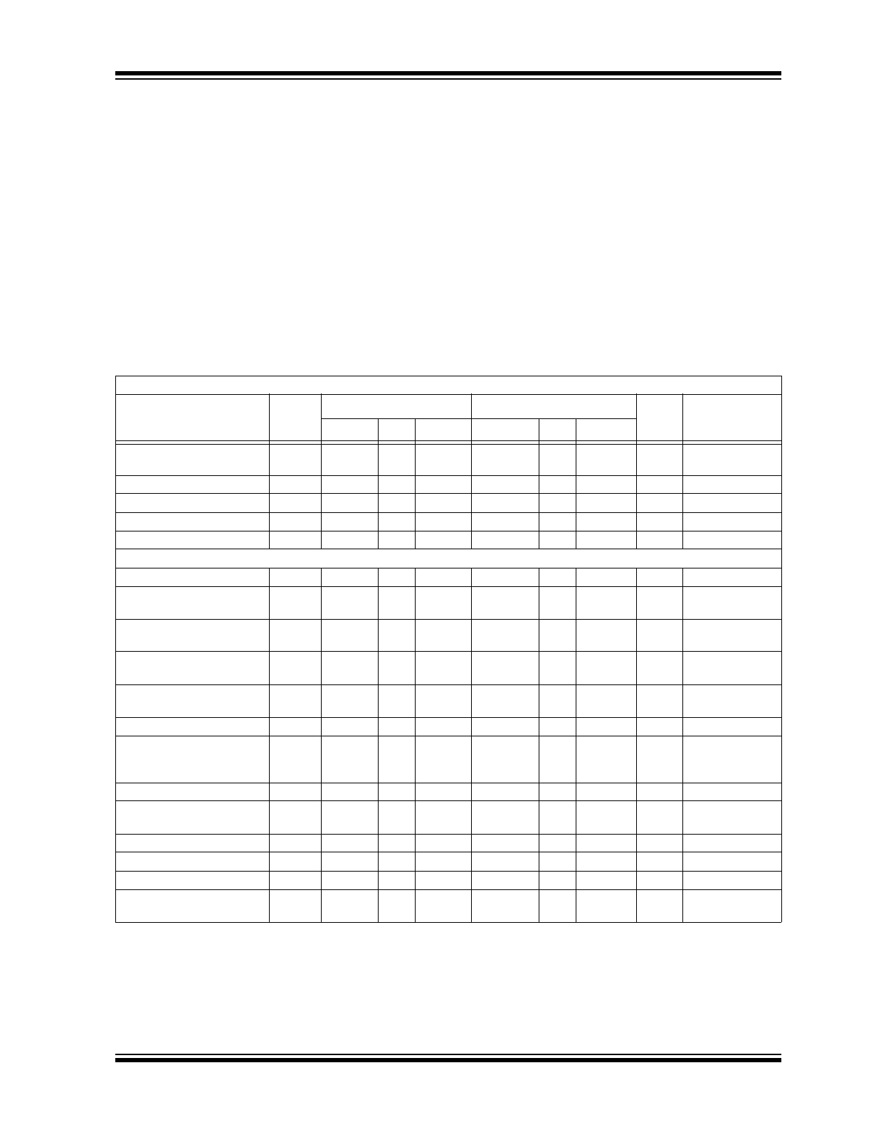
ELECTRICAL SPECIFICATIONS
Electrical Characteristics: Unless otherwise specifier, V
DD
= V
CCD
, C
AZ
= C
REF
= 0.47 µF
Parameter
Symbol
T
A
= +25°C
T
A
= 0°C to +70°C
Unit
Conditions
Min
Typ
Max
Min
Typ
Max
Analog Power Supply
Voltage
V
DD
4.5
5.0
5.5
4.5
—
5.5
V
Digital Power Supply Voltage
V
CCD
4.5
5.0
5.5
4.5 —
5.5
V
Total Power Dissipation
P
D
—
—
25
—
—
—
mW
V
DD
= V
CCD
= 5V
Supply Current (V
S
+ P
IN
)
I
S
—
1.8
2.5
—
—
3.0
mA
Supply Current (V
CCD
P
IN
)
I
CCD
—
—
1.5
—
—
1.7
mA
F
OSC
= 1 MHz
Analog
Resolution
R
—
—
±17
—
—
±17
Bits
Note 1
Zero Scale Error with Auto
Zero Phase
ZSE
—
—
0.5
—
0.005
0.012
% F.S.
End Point Linearity
ENL
—
0.015
0.030
—
0.015 0.045
%
F.S. Note 1 and
Note 2
Max. Deviation from Best
Straight Line Fit
NL
—
0.008
0.015
— —
—
%
F.S. Note 1 and
Note 2
Zero Scale Temperature
Coefficient
ZS
TC
—
—
—
—
1
2
µV/°C
Rollover Error
SYE
—
.012
—
—
.03
—
% F.S. Note 3
Full Scale Temperature
Coefficient
FS
TC
—
—
—
—
10
—
ppm/°
C
Ext. V
REF
T.C. = 0 ppm/°C
Input Current
I
IN
—
6
—
—
—
—
pA
V
IN
= 0V
Common-Mode Voltage
Range
V
CMR
V
SS
+ 1.5
—
V
DD
- 1.5 V
SS
+ 1.5
—
V
DD
- 1.5
V
Integrator Output Swing
V
INT
V
SS
+ 0.9
—
V
DD
- 0.9 V
SS
+ 0.9
—
V
DD
- 0.9
V
Analog Input Signal Range
V
IN
V
SS
+ 1.5
—
V
DD
-1.5
V
SS
+ 1.5
—
V
DD
- 1.5
V
Voltage Reference Range
V
REF
V
SS
+ 1
—
V
DD
- 1
V
DD
+ 1
—
V
DD
- 1
V
Zero Crossing Comparator
Delay
T
D
—
2.0
—
—
3.0
—
μs
Note 1: Integrate time
≥ 66 ms. Auto Zero time ≥ 66 ms. V
INT
(pk) = 4V.
2: End point linearity at ±1/4, ±1/2, and ±3/4. F.S. after full scale adjustment.
3: Rollover error is related to capacitor used for CINT. See
Table 6-2
, Recommended Capacitor for C
INT
.
4: TC534 Only.
TC530/TC534
DS21433C-page 4
© 2007 Microchip Technology Inc.
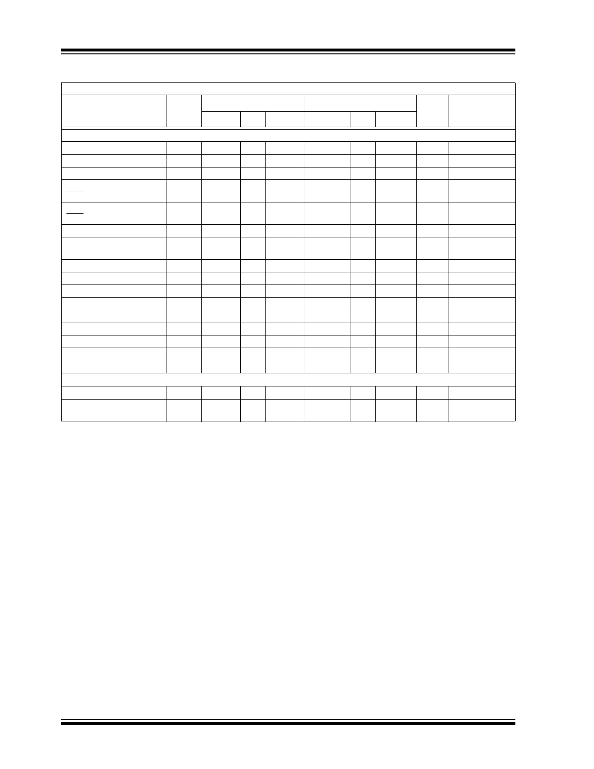
Serial Port Interface
Input Logic HIGH Level
V
IH
2.5
—
—
2.5
—
—
V
Input Logic LOW Level
V
IL
—
—
0.8
—
—
0.8
V
Input Current (DI, DO, D
CLK
)
I
IN
—
—
10
—
—
—
µA
Logic LOW Output Voltage
(EOC)
V
OL
—
0.2
0.3
—
—
0.35
V
I
OUT
= 250 µA
Rise and Fall Times
(EOC, DI, DO)
T
R
, T
F
—
—
250
—
250
ns
C
L
= 10 pF
Crystal Frequency
F
XTL
—
—
2.0
—
—
2.0
MHz
External Frequency on
OSC
IN
F
EXT
—
—
4.0
—
—
4.0
MHz
Read Setup Time
T
RS
1
—
—
—
1
—
µs
Read Delay Time
T
RD
250
—
—
—
250
ns
D
CLK
to D
OUT
Delay
T
DRS
450
—
—
—
450
ns
D
CLK
LOW Pulse Width
T
PWL
150
—
—
—
150
ns
D
CLK
HIGH Pulse Width
T
PWH
150
—
—
—
150
ns
Data Ready Delay
T
DR
200
—
—
—
200
ns
Output Resistance
R
OUT
—
65
85
—
—
100
Ω
I
OUT
= 10 mA
Oscillator Frequency
F
CLK
—
100
—
—
—
—
kHz
C
OSC
= 0
V
SS
Output Current
I
OUT
—
—
10
—
—
10
mA
Multiplexer
Maximum Input Voltage
V
IMMAX
-2.5
—
2.5
-2.5
—
2.5
V
Drain/Source ON
Resistance
R
DSON
—
6
10
—
—
—
k
Ω
ELECTRICAL SPECIFICATIONS (CONTINUED)
Electrical Characteristics: Unless otherwise specifier, V
DD
= V
CCD
, C
AZ
= C
REF
= 0.47 µF
Parameter
Symbol
T
A
= +25°C
T
A
= 0°C to +70°C
Unit
Conditions
Min
Typ
Max
Min
Typ
Max
Note 1: Integrate time
≥ 66 ms. Auto Zero time ≥ 66 ms. V
INT
(pk) = 4V.
2: End point linearity at ±1/4, ±1/2, and ±3/4. F.S. after full scale adjustment.
3: Rollover error is related to capacitor used for CINT. See
Table 6-2
, Recommended Capacitor for C
INT
.
4: TC534 Only.
© 2007 Microchip Technology Inc.
DS21433C-page 5
TC530/TC534
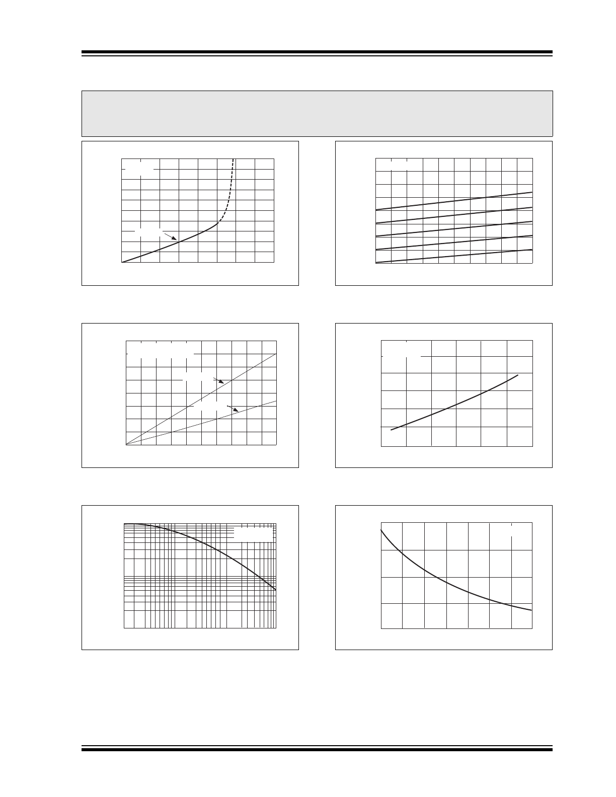
2.0
TYPICAL PERFORMANCE CURVES
FIGURE 2-1:
Output Voltage vs. Load
Current.
FIGURE 2-2:
Output Ripple vs. Load
Current.
FIGURE 2-3:
Oscillator Frequency vs.
Capacitance.
FIGURE 2-4:
Output Voltage vs. Output
Current.
FIGURE 2-5:
Output Source Resistance
vs. Temperature.
FIGURE 2-6:
Oscillator Frequency vs.
Temperature.
Note:
The graphs and tables provided following this note are a statistical summary based on a limited number of
samples and are provided for informational purposes only. The performance characteristics listed herein
are not tested or guaranteed. In some graphs or tables, the data presented may be outside the specified
operating range (e.g., outside specified power supply range), and therefore outside the warranted range.
LOAD CURRENT (mA)
-5
-4
-3
-2
-1
0
1
2
3
4
5
0
10
20
30
40
50
60
70
80
OUTPUT VOLTAGE (V)
Output Voltage vs. Load Current
T
A
= 25
˚
C
V+ = 5V
Slope 60
Ω
LOAD CURRENT (mA)
0
3
4
5
6
1
2
7
8
9
10
0
25
50
75
100
125
150
175
200
OUTPUT RIPPLE (mV PK-PK)
Output Ripple vs. Load Current
V+ = 5V, T
A
= 25˚C
Osc. Freq. = 100kHz
CAP = 1
μ
F
CAP = 10
μ
F
OSCILLATOR CAPACITANCE (pF)
100
10
1
1
10
100
1000
OSCILLATOR FREQUENCY (kHz)
Oscillator Frequency vs. Capacitance
T
A
= +25˚C
V+ = 5V
OUTPUT CURRENT (mA)
0
6
8
10
4
2
14
16
18
12
20
-0
-1
-3
-2
-4
-5
-7
-6
-8
Output Voltage vs. Output Current
T
A
= 25˚C
OUTPUT VOLTAGE (V)
TEMPERATURE (˚C)
70
80
90
100
60
50
40
-50
0
25
-25
50
75
100
OUTPUT SOURCE RESISTANCE (
Ω
)
Output Source Resistance vs. Temperature
V+ = 5V
I
OUT
= 10mA
TEMPERATURE (˚C)
125
150
100
75
50
-50
0
25
-25
50
75
125
100
OSCILLATOR FREQUENCY (kHz)
Oscillator Frequency vs. Temperature
V+ = 5V
TC530/TC534
DS21433C-page 6
© 2007 Microchip Technology Inc.
3.0
PIN DESCRIPTIONS
The descriptions of the pins are listed in
Table 3-1
.
TABLE 3-1:
PIN FUNCTION TABLE
Pin Number
(TC530)
28-Pin PDIP
Pin Number
(TC530)
28-Pin SOIC
Pin Number
(TC534)
40-Pin PDIP
Pin
Number
(TC534)
44-Pin
MQFP
Sym
Description
1
1
1
40
V
SS
Analog output. Negative power supply converter output and
reservoir capacitor connection. This output can be used to
provide negative bias to other devices in the system.
2
2
2
41
C
INT
Analog output. Integrator capacitor connection and
integrator output.
3
3
3
42
C
AZ
Analog input. Auto Zero capacitor connection.
4
4
4
43
BUF
Analog output. Integrator capacitor connection and voltage
buffer output.
5
5
5
2
ACOM
Analog input. This pin is ground for all of the analog
switches in the A/D converter. It is grounded for most
applications. ACOM and the input common pin (V
IN
- or
CHX-) should be within the common mode range, CMR.
6
6
6
3
C
REF
-
Analog Input. Reference cap negative connection.
7
7
7
4
C
REF
+
Analog Input. Reference cap positive connection.
8
8
8
5
V
REF
-
Analog Input. External voltage reference negative
connection.
9
9
9
6
V
REF
+
Analog Input. External voltage reference positive
connection.
—
—
10
7
CH4-
Analog Input. Multiplexer channel 4 negative differential
—
—
11
8
CH3-
Analog Input. Multiplexer channel 3 negative differential
—
—
12
9
CH2-
Analog Input. Multiplexer channel 2 negative differential
—
—
13
10
CH1-
Analog Input. Multiplexer channel 1 negative differential
—
—
14
11
CH4+
Analog Input. Multiplexer channel 4 positive differential
—
—
15
12
CH3+
Analog Input. Multiplexer channel 3 positive differential
—
—
16
13
CH2+
Analog Input. Multiplexer channel 2 positive differential
—
—
17
14
CH1+
Analog Input. Multiplexer channel 1 positive differential
10
10
—
—
V
N
-
Analog Input. Negative differential analog voltage input.
11
11
—
—
V
IN
+
Analog Input. Positive differential analog voltage input.
12
12
18
15
DGND
Analog Input. Ground connection for serial port circuit.
—
—
19
16
A1
Logic Level Input. Multiplexer address MSB.
—
—
20
17
A0
Logic Level Input. Multiplexer address LSB.
14
14
21
18
OSC
OUT
Analog Input. Timebase for state machine. This pin
connects to one side of an AT-cut crystal having an effective
series resistance of 100
Ω (typ) and a parallel capacitance
of 20 pF. If an external frequency source is used to clock
the TC530/TC534 this pin must be left floating.
15
15
22
19
OSC
IN
Analog Input. This pin connects to the other side of the
crystal described in OSC
OUT
above. The TC530/TC534
may also be clocked from an external frequency source
connected to this pin. The external frequency source must
be a pulse waveform with a minimum 30% duty cycle and
rise and fall times 15nsec (Max). If an external frequency
source is used, OSC
OUT
) must be left floating. A maximum
operating frequency of 2 MHz (crystal) or 4 MHz (external
clock source) is permitted.
© 2007 Microchip Technology Inc.
DS21433C-page 7
TC530/TC534
16
16
23
20
D
OUT
Logic Level Output. Serial port data output pin. This pin is
enabled only when R/W is high.
17
17
24
21
D
CLK
Logic Input, Positive and Negative Edge Triggered. Serial
port clock. When R/W is high, serial data is clocked out of
the TC530/TC534A (on D
OUT
) at each high-to-low transition
of D
CLK
. A/D initialization data (LOAD VALUE) is clocked
into the TC530/TC534 (on D
IN
) at each low-to-high
transition of D
CLK
. A maximum serial port D
CLK
frequency
of 3 MHz is permitted.
18
18
25
22
D
IN
Logic Level Input. Serial port input pin. The A/D converter
integration time (T
INT
) and Auto Zero time (T
AZ
) values are
determined by the LOAD VALUE byte clocked into this pin.
This initialization must take place at power up, and can be
rewritten (or modified and rewritten) at any time. The LOAD
VALUE is clocked into D
IN
MSB first.
19
19
26
23
R/W
Logic Level Input. This pin must be brought low to perform a
write to the serial port (e.g. initialize the A/D converter). The
D
OUT
pin of the serial port is enabled only when this pin is
high.
20
20
27
24
EOC
Open Drain Output. End-of-Conversion (EOC) is asserted
any time the TC530/TC534 is in the AZ phase of
conversion. This occurs when either the TC530/TC534
initiates a normal AZ phase or when RESET is pulled high.
EOC is returned high when the TC530/TC534 exits AZ.
Since EOC is driven low immediately following completion
of a conversion cycle, it can be used as a DATA READY
processor interrupt.
21
21
30
28
RESET
Logic Level Input. It is necessary to force the TC530/TC534
into the Auto Zero phase when power is initially applied.
This is accomplished by momentarily taking RESET high.
Using an I/O port line from the microprocessor or by
applying an external system reset signal or by connecting a
0.01 µF capacitor from the RESET input to V
DD
. Conver-
sions are performed continuously as long as RESET is low
and conversion is halted when RESET is high. RESET may
therefore be used in a complex system to momentarily
suspend conversion (for example, while the address lines
of an input multiplexer are changing state). In this case,
RESET should be pulled high only when the EOC is LOW
to avoid excessively long integrator discharge times which
could result in erroneous conversion. (See Applications
Section).
22
22
32
30
V
CCD
Analog Input. Power supply connection for digital logic and
serial port. Proper power-up sequencing is critical, see the
Applications section.
23
23
34
32
OSC
Input. The negative power supply converter normally runs
at a frequency of 100 kHz. This frequency can be slowed
down to reduce quiescent current by connecting an external
capacitor between this pin and V
+
DD.
See Section 2.0 “Typical Performance Curves”, Typical
Characteristics.
25
25
37
35
V
DD
Analog Input. Power supply connection for the A/D analog
section and DC-DC converter. Proper power-up sequencing
is critical, (See the Applications section).
TABLE 3-1:
PIN FUNCTION TABLE (CONTINUED)
Pin Number
(TC530)
28-Pin PDIP
Pin Number
(TC530)
28-Pin SOIC
Pin Number
(TC534)
40-Pin PDIP
Pin
Number
(TC534)
44-Pin
MQFP
Sym
Description

TC530/TC534
DS21433C-page 8
© 2007 Microchip Technology Inc.
26
26
38
36
CAP+
Analog Input. Storage capacitor positive connection for the
DC/DC converter.
27
27
39
37
AGND
Analog Input. Ground connection for DC/DC converter.
28
28
40
38
CAP-
Analog Input. Storage capacitor negative connection for the
DC/DC converter.
13, 24
13, 24
28, 29, 31,
33, 35, 36
1, 25, 26,
27, 29, 31,
33, 34, 39,
44
N/C
No connect. Do not connect any signal to these pins.
TABLE 3-1:
PIN FUNCTION TABLE (CONTINUED)
Pin Number
(TC530)
28-Pin PDIP
Pin Number
(TC530)
28-Pin SOIC
Pin Number
(TC534)
40-Pin PDIP
Pin
Number
(TC534)
44-Pin
MQFP
Sym
Description
© 2007 Microchip Technology Inc.
DS21433C-page 9
TC530/TC534
4.0
DETAILED DESCRIPTION
4.1
Dual Slope Integrating Converter
The TC530/TC534 dual slope converter operates by
integrating the input signal for a fixed time period, then
applying an opposite polarity reference voltage while
timing the period (counting clocks pulses) for the
integrator output to cross 0V (deintegrating). The
resulting count is read as conversion data.
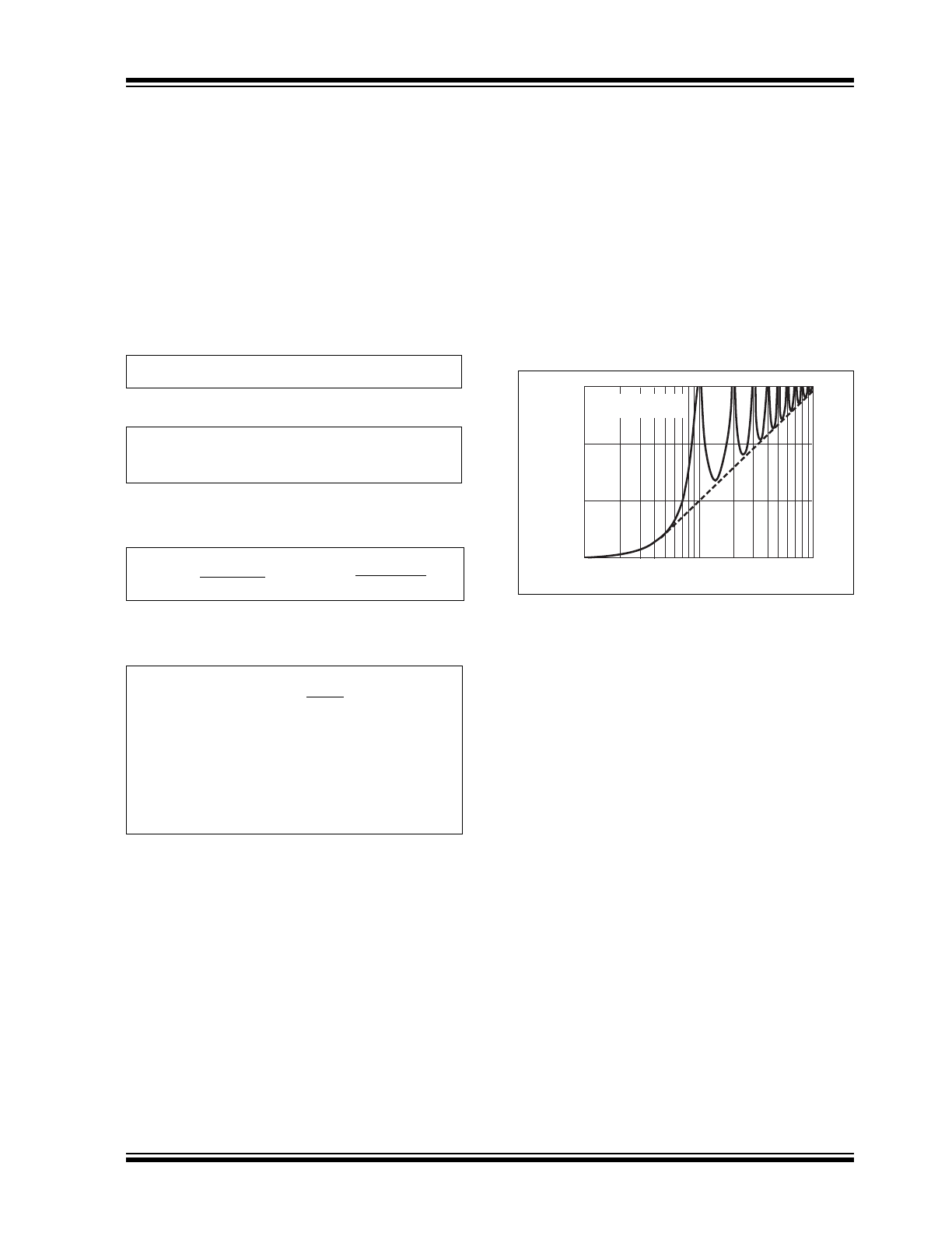
A simple mathematical expression that describes dual
slope conversion is:
EQUATION 4-1:
EQUATION 4-2:
from which:
EQUATION 4-3:
And therefore:
EQUATION 4-4:
Inspection of
Equation 4-4
shows dual slope converter
accuracy is unrelated to integrating resistor and
capacitor values, as long as they are stable throughout
the measurement cycle. This measurement technique
is inherently ratiometric (i.e., the ratio between the T
INT
and T
DEINT
times is equal to the ratio between V
IN
and
V
REF
).
Another inherent benefit is noise immunity. Input noise
spikes are integrated, or averaged to zero, during the
integration period. The integrating converter has a noise
immunity with an attenuation rate of at least -20 dB per
decade. Interference signals with frequencies at integral
multiples of the integration period are, for the most part,
completely removed. For this reason, the integration
period of the converter is often established to reject
50/60 Hz line noise. The ability to reject such noise is
shown by the plot of
Figure 4-1
.
In addition to the two phases required for dual slope
measurement (Integrate and De-integrate), the
TC530/TC534 performs two additional adjustments to
minimize measurement error due to system offset volt-
ages. The resulting four internal operations (conver-
sion phases) performed each measurement cycle are:
Auto Zero (AZ), Integrator Output Zero (IZ), Input
Integrate (INT) and Reference De-integrate (DINT).
The AZ and IZ phases compensate for system offset
errors and the INT and DINT phases perform the actual
A/D conversion.
FIGURE 4-1:
Integrating Converter
Normal Mode Rejection.
4.2
Auto Zero Phase (AZ)
This phase compensates for errors due to buffer,
integrator and comparator offset voltages. During this
phase, an internal feedback loop forces a
compensating error voltage on auto zero capacitor
(C
AZ
). The duration of the AZ phase is programmable
via the serial port (see Section 5.1.1 “AZ and INT
Phase Duration”, AZ and INT Phase Duration).
Integrate Voltage = De-integrate Voltage
1
R
INT
C
INT
------------------------ T
INT
0
∫
V
IN
T
( )dT
1
R
INT
C
INT
------------------------ T
DEINT
0
∫
V
REF
=
(V
IN
)
(R
INT
)(C
INT
)
[
(T
INT
)
= (V
REF
)
]
(R
INT
)(C
INT
)
[
(T
DEINT
)
]
V
IN
= V
REF
[ ]
T
INT
T
DEINT
Where:
V
REF
=
Reference Voltage
T
INT
=
Integrate Time
T
DEINT
=
Reference Voltage De-integrate
Time
30
20
10
0
0.1/T
1/T
10/T
Input Frequency
Normal Mode Rejection (dB)
T = Measurement
Period
TC530/TC534
DS21433C-page 10
© 2007 Microchip Technology Inc.
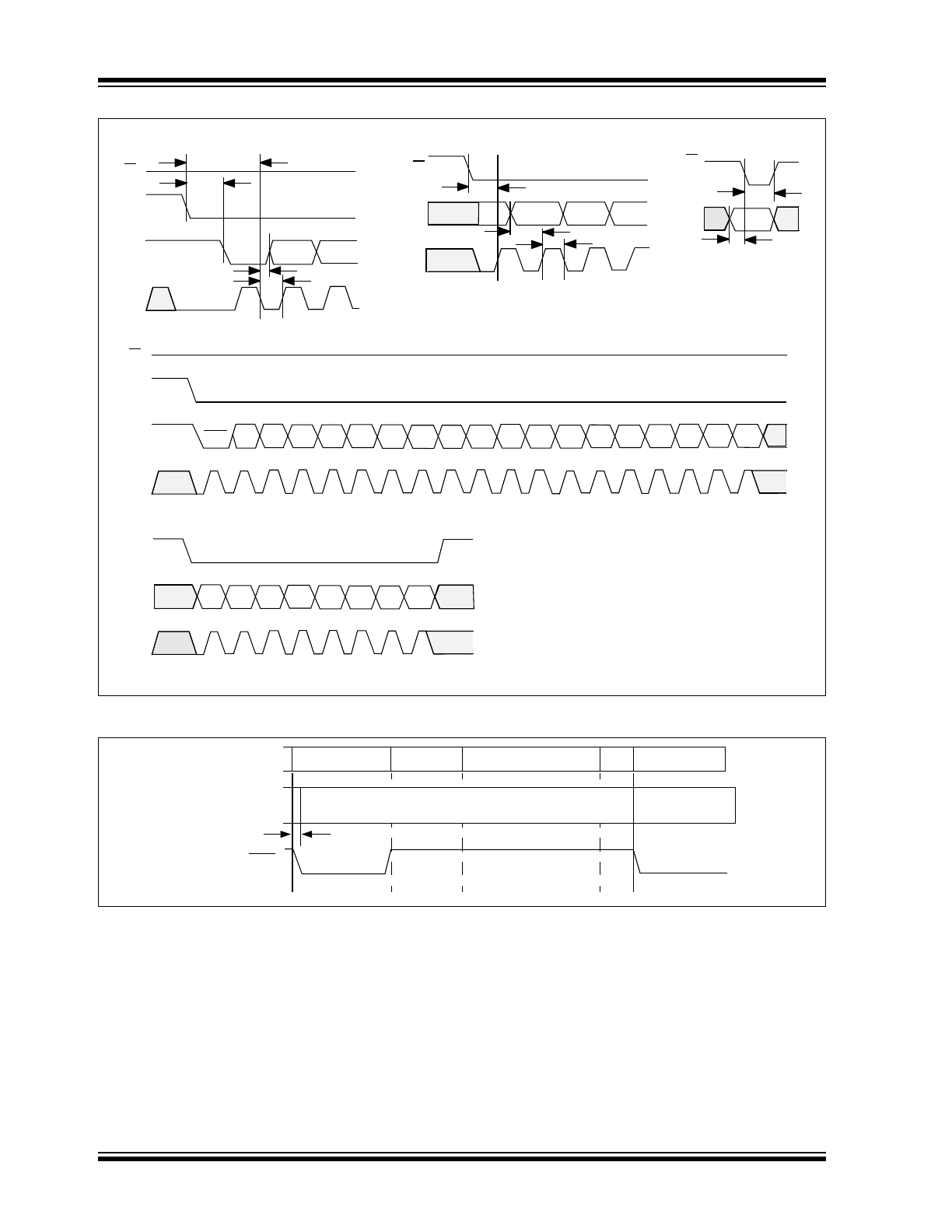
FIGURE 4-2:
Serial Port Timing.
FIGURE 4-3:
A/D Converter Timing.
T
RD
T
RS
T
DRS
T
PWL
R/W
Read Timing
Read Format
Write Format
Write Timing
Write Default Timing
EOC
D
OUT
D
CLK
R/W
EOC
D
OUT
D
CLK
EOC
SGN MSB
LSB
OVR
T
LS
T
DLS
T
PWL
R/W
D
IN
D
CLK
T
LDL
T
LDS
D
IN
R/W
D
OUT
D
CLK
MSB
LSB
For Polled vs. Interrupt Operation and Write Value Modified Cycle Use TC520A Data Sheet (DS21431).
R/W
EOC
T
DR
AZ
Updated Data
Ready
Updated Data
Ready
INT
DINT
IZ
AZ
Conversion
Phase
Data to Serial
Port Transmit
Register