
2001-2012 Microchip Technology Inc.
DS21431C-page 1
TC520A
Features
• Converts TC500/TC500A/TC510/TC514 to Serial
Operation
• Programmable Conversion Rate and Resolution for
Maximum Flexibility
• Supports up to 17-Bits of Accuracy Plus Polarity Bit
• Low Power Operation: Typically 7.5m
• 14-Pin PDIP or 16-Pin SOIC Packages
• Polled or Interrupt Mode Operation
Applications
• Computer Peripheral Interface
• Portable Instruments
• Data Acquisition System Interface
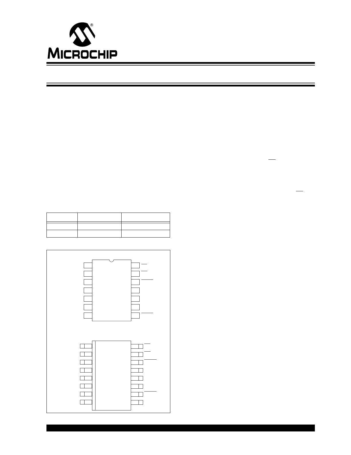
Device Selection Table
Package Type
General Description
The TC520A serial interface adapter provides logic
control for Microchip's TC500/TC500A/TC510/TC514
family of dual slope, integrating A/D converters. It
directly manages TC500 converter phase control sig-
nals A, B and CMPTR, thereby reducing host
processor task loading and software complexity. Com-
munication with the TC520A is accomplished over a 3
wire serial port. Key converter operating parameters
are programmable for complete user flexibility. Data
conversion is initiated when the CE input is brought
low. The converted data (plus overrange and polarity
bits) are held in an 18-bit shift register until read by the
processor or until the next conversion is completed.
Data may be clocked out of the TC520A at any time,
and at any rate, the user prefers. A Data Valid (DV) out-
put is driven active at the start of each conversion
cycle, indicating the 18-bit shift register update has just
been completed. This signal may be polled by the pro-
cessor or can be used as data ready interrupt. The
TC520A timebase can be derived from an external fre-
quency source of up to 6MHz or can operate from its
own external crystal. It requires a single 5V logic supply
and dissipates less than 7.5m
.
Part Number
Package
Temperature Range
TC520ACOE 16-Pin SOIC (Wide)
0
C to +70C
TC520ACPD
14-Pin PDIP
0
C to +70C
B
CMPTR
DGND
V
DD
A
D
IN
OSC
OUT
DCLK
OSC
IN
D
OUT
1
14
2
13
3
12
4
11
5
10
6
9
7
8
TC520A
CE
DV
LOAD
READ
14-Pin PDIP
16-Pin SOIC
8
1
2
3
4
5
6
7
TC520A
D
IN
B
14
13
12
11
10
9
15
16
LOAD
DV
CE
DCLK
A
D
OUT
READ
N/C
CMPTR
DGND
V
DD
OSC
OUT
OSC
IN
N/C
Serial Interface Adapter for TC500 A/D Converter Family
TC520A
DS21431C-page 2
2001-2012 Microchip Technology Inc.
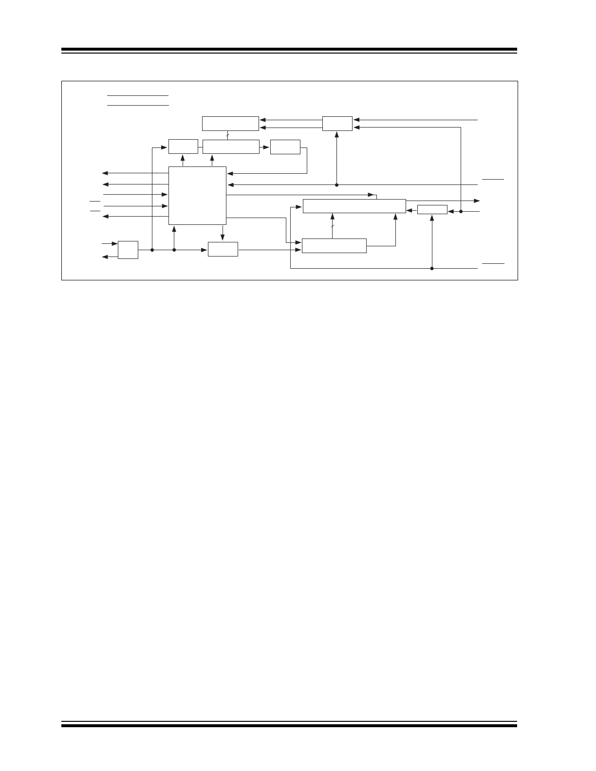
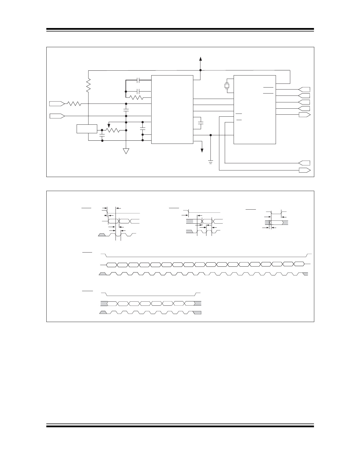
Functional Block Diagram
Logic Control
Gate
8-Bit Counter
÷ 256
8-Bit Shift Reg.
÷4
Gate
Pinout of 14-Pin
Package
7
SYSCLK
8
6
A
B
CMPTR
CE
DV
5
4
3
14
13
Gate
Timeout
Force Auto Zero
Polarity Bit
Clear Count
1
2
V
DD
GND
16-Bit Counter
18-Bit Shift Register
Gate
Overrange
Bit
11
12
9
10
8
DCLK
D
OUT
D
IN
LOAD
READ
16
OSC
IN
OSC
OUT
2001-2012 Microchip Technology Inc.
DS21431C-page 3
TC520A
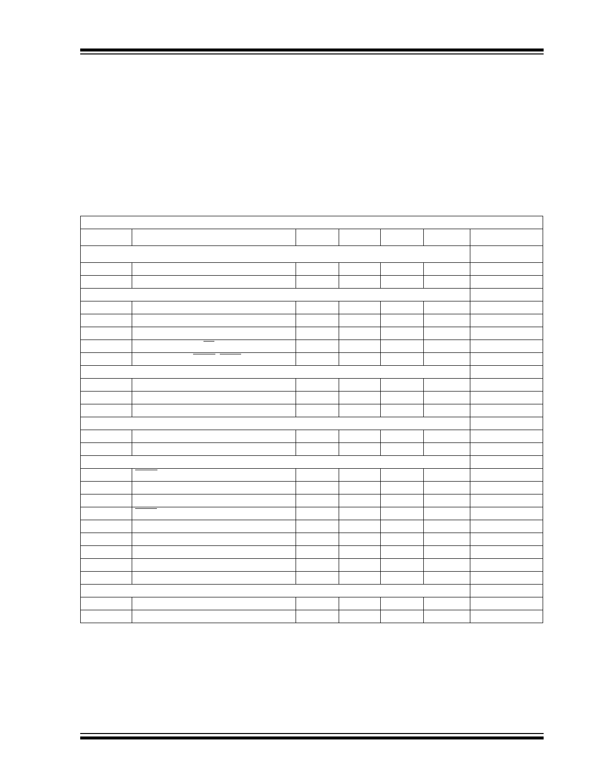
1.0
ELECTRICAL
CHARACTERISTICS
Absolute Maximum Ratings*
DC Supply Voltage (V
DD
) .................................... +6.0V
Input Voltage (All Inputs V
IN
):.... - 0.3V to (V
DD
+ 0.3V)
Operating Temperature Range (T
A
) .......... 0°C to 70°C
Storage Temperature Range .............. -65°C to +150°C
*Stresses above those listed under "Absolute Maximum Rat-
ings" may cause permanent damage to the device. These are
stress ratings only and functional operation of the device at
these or any other conditions above those indicated in the
operation sections of the specifications is not implied. Expo-
sure to Absolute Maximum Rating conditions for extended
periods may affect device reliability.
TC520A ELECTRICAL SPECIFICATIONS
Electrical Characteristics: V
DD
= 5V, F
OSC
= 1MHz, T
A
= +25°C, unless otherwise specified.
Symbol
Parameters
Min
Typ
Max
Unit
Test Conditions
Supply
V
DD
Operating Voltage Range
4.5
5
5.5
V
I
DD
Supply Current
—
0.8
1.5
mA
Input Characteristics
V
IL
Low Input Voltage
—
—
0.8
V
V
IH
High Input Voltage
2.0
—
—
V
I
IL
Input Leakage Current
—
—
10
A
I
PD
Pull-down Current (CE)
—
5
—
A
I
PU
Pull-up Current (READ, LOAD) —
5
—
A
Output Characteristics (I
OUT
= 250
A, V
DD
= 5V)
V
OL
Low Output Voltage
—
0.2
0.3
V
V
OH
High Output Voltage
3.5
4.3
—
V
T
R
, T
F
C
L
= 10pF, Rise/Fall Times
—
—
250
nsec
Oscillator (OSC
IN
, OSC
OUT
)
F
XTL
Crystal Frequency
—
1.0
4.0
MHz
F
OSC
External Frequency (OSC
IN
)
—
—
6.0
MHz
Timing Characteristics
T
RD
READ Delay Time
250
—
—
nsec
T
RS
Data Read Setup Time
1
—
—
sec
T
DRS
D
CLK
to D
OUT
Delay
450
—
—
nsec
T
LS
LOAD Setup Time
1
—
—
sec
T
DLS
Data Load Setup Time
50
—
—
nsec
T
PWL
D
CLK
Pulse Width Low Time
150
—
—
nsec
T
PWH
D
CLK
Pulse Width High Time
150
—
—
nsec
T
LDL
Load Default Low Time
250
—
—
nsec
T
LDS
Load Default Setup Time
250
—
—
nsec
Parameter
T
IZ
Integrator ZERO Time
—
0.5
—
msec
T
AZI
Auto zero (RESET) Time at Power-Up
—
100
—
msec
TC520A
DS21431C-page 4
2001-2012 Microchip Technology Inc.
2.0
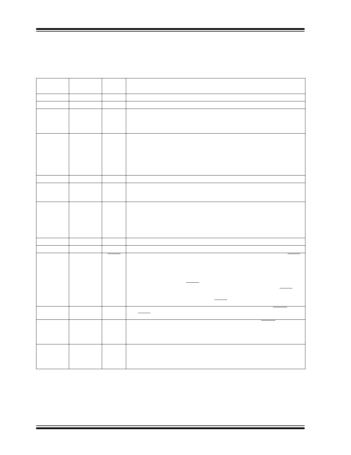
PIN DESCRIPTIONS
The descriptions of the pins are listed in Table 2-1
TABLE 2-1:
PIN FUNCTION TABLE
Pin Number
14-Pin PDIP
Pin Number
16-Pin SOIC
Symbol
Description
1
1
V
DD
Input. +5V ±10% power supply input with respect to DGND.
2
2
DGND
Input. Digital Ground.
3
3
CMPTR
Input, active high or low (depending on polarity of the voltage input to A/D converter).
This pin connects directly to the zero crossing comparator output (CMPTR) of the
TC5XX A/D converter. A high-to-low state change on this pin causes the TC520A to
terminate the de-integrate phase of conversion.
4
4
B
Output, active high. The A and B outputs of the TC520A connect directly to the A and B
inputs of the TC5XX A/D converter connected to the TC520A. The binary code on A, B
determines the conversion phase of the TC5XX A/D converter: (A, B) = 01 places the
TC5XX A/D converter into the Auto Zero phase; (A, B) =10 for Integrate phase (INT);
(A, B) =11 for De-integrate phase (DINI) and (A, B) = 00 for Integrator Zero phase (IZ).
Please see the TC500/TC500A/TC510/TC514 family data sheets for a complete
description of these phases of operation.
5
5
A
Output, active high. See pin 4 description above.
6
6
OSC
OUT
Input. This pin connects to one side of an AT-cut crystal having a effective series resis-
tance of 100
(typ.) and a parallel capacitance of 20pF (typ.). If an external frequency
source is used to clock the TC520A, this pin must be left floating.
7
7
OSC
IN
Input. This pin connects to the other side of the crystal described in pin 6 above. The
TC520A may also be clocked from an external frequency source connected to this pin.
The external frequency source must be a pulse train having a duty cycle of 30% (mini-
mum); rise and fall times of 15nsec and a min/max amplitude of 0 to V
IH
. If an external
frequency source is used, pin 6 must be left floating. A maximum operating frequency
of 4MHz (crystal) or 6MHz (external clock source) is permitted.
8
N/C
No connection on 16 pin package version.
9
N/C
No connection on 16 pin package version.
8
10
READ
Input, active low, level and negative edge triggered. A high-to-low transition on READ
loads serial port output shift register with the most recent converted data. Data is
loaded such that the first bit transmitted from the TC520A to the processor is the
OVERRANGE bit (OVR), followed by the POLARITY bit (POL) (high = input positive;
low = input negative). This is followed by a 16-bit data word (MSB first). OVR is avail-
able at the D
OUT
as soon as READ is brought low. This bit may be used as the 17th
data bit, if so desired. The D
OUT
pin of the serial port is enabled only when READ is
held low. Otherwise, D
OUT
remains in a high impedance state. A serial port read access
cycle is terminated at any time by bringing READ high.
9
11
D
OUT
Output, logic level. Serial port output pin. This pin is enabled only when READ is low
(see READ pin description).
10
12
D
CLK
Input, positive and negative edge triggered. Serial port clock. With READ low, serial
data is clocked into the TC520A at each low-to-high transition of D
CLK
, and clocked out
of the TC520A on each high-to-low transition of D
CLK
. A maximum serial port D
CLK
frequency of 3MHz is permitted.
11
13
D
IN
Input, logic level. Serial port input pin. The TC5XX A/D converter integration time (T
INT
)
and Auto Zero time (TAZ) values are determined by the LOAD VALUE byte clocked into
this pin. This initialization must take place at power up and can be rewritten (or modified
and rewritten) at any time. The LOAD VALUE is clocked into D
IN
MSB first.
2001-2012 Microchip Technology Inc.
DS21431C-page 5
TC520A
12
14
LOAD
Input, active low; level and edge triggered. The LOAD VALUE is clocked into the 8-bit
shift register on board the TC520A while LOAD is held low. The LOAD VALUE is then
transferred into the TC520A internal timebase counter (and becomes effective) when
LOAD is returned high. If so desired, LOAD can be momentarily pulsed low, eliminating
the need to clock a LOAD VALUE into D
IN
. In this case, the current state of D
IN
is
clocked into the TC520A timebase counter selecting either a count of 65536
(D
IN
= High), or count of 32768, (D
IN
= Low).
13
15
DV
Output, active low. DV is brought low any time the TC520A is in the AZ phase of con-
version. This occurs when, either the TC520A initiates a normal AZ phase by setting A,
B, equal to 01, or when CE is pulled high, which overrides the normal A, B sequencing
and forces an AZ state. DV is returned high when the TC520A exits AZ.
14
16
CE
Input, active low, level triggered. Conversion will be continuously performed as long as
CE remains low. Pulling CE high causes the conversion process to be halted and
forces the TC520A into the AZ mode for as long as CE remains high. CE should be
taken high whenever it is necessary to momentarily suspend conversion (for example:
to change the address lines of an input multiplexer). CE should be pulled high only
when the TC520A enters an AZ phase (i.e. when DV is low). This is necessary to avoid
excessively long integrator discharge times, which could result in erroneous conver-
sion. This pin should be grounded if unused. It should be left floating if a 0.01
F
RESET capacitor is connected to it (see Section 4.0, Typical Applications).
TABLE 2-1:
PIN FUNCTION TABLE (CONTINUED)
Pin Number
14-Pin PDIP
Pin Number
16-Pin SOIC
Symbol
Description

TC520A
DS21431C-page 6
2001-2012 Microchip Technology Inc.
3.0
DETAILED DESCRIPTION
3.1
TC520A Timing
The TC520A consists of a serial port and state
machine. The state machine provides control timing to
the TC5xx A/D converter connected to the TC520A as
well as providing sequential timing for TC520A internal
operation. All timing is derived from the frequency
source at OSC
IN
and OSC
OUT
. This frequency source
can be either an externally provided clock signal or
external crystal. If an external clock is used, it must be
connected to the OSC
IN
pin and OSC
OUT
must remain
floating. If a crystal is used, it must be connected
between the OSC
IN
and OSC
OUT
and be physically
located as close to the OSC
IN
and OSC
OUT
pins as
possible. The incoming frequency is internally divided
by 4 and the resulting clock (SYSCLK) controls all
timing functions.
3.2
TC5XX A/D Converter Control
Signals
The TC520A control outputs (A, B) and control input
(CMPTR) connect directly to the corresponding pins of
the TC5XX A/D converter. A conversion is consum-
mated when A, B have been sequenced through the
required 4 phases of conversion: Auto Zero (AZ), Inte-
grate (INT), De-integrate (D
INT
) and Integrator Zero (IZ)
(see Figure 4-1). The Auto Zero phase compensates
for offset errors in the TC5XX A/D converter. The
Integrate phase connects the voltage to be converted
to the TC5XX A/D converter input, resulting in an inte-
grator output dv/dt directly proportional to the magni-
tude of the applied input voltage. Actual A/D conversion
(counting) is initiated at the start of the DINT phase and
terminates when the integrator output crosses 0V. The
integrator output is then forced to 0V during the IZ
phase and the converter is ready for another cycle.
Please see the TC500/TC500A/TC510/TC514 data
sheet for a complete description of these phases.
The number of SYSCLK periods (counts) for the AZ
and INT phases is determined by the LOAD VALUE.
The LOAD VALUE is a single byte that must be loaded
into the most significant byte of 16-bit counter on board
the TC520A during initialization. The lower byte of this
counter is pre-loaded to a value of 0FFH (256
10
) and
cannot be changed.
The LOAD VALUE (upper 8 bits of the counter) can be
programmed over a range of 0FFH to 00H (corre-
sponding to a range of AZ = INT = 256 counts to 65536
counts). (See Figure 3-2). The LOAD VALUE sets the
number of counts for both the AZ and INT phases and
directly affects resolution and speed of conversion. The
greater the number of counts allowed for AZ and INT,
the greater the A/D resolution (but the slower the con-
version speed).
The time period required for the DINT phase is a func-
tion of the amount of voltage stored on the integrator
during the INT phase and the value of V
REF
. The DINT
phase is initiated by the TC520A immediately after the
INT phase and terminated when the TC5XX A/D con-
verter changes the state of the CMPTR input of the
TC520A, indicating a zero crossing. In general, the
maximum number of counts chosen for DINT is twice
that of INT (with V
REF
chosen at V
ININ(MAX)
/2). Choos-
ing these values guarantees a full count (maximum res-
olution) during D
INT
when V
IN
= V
IN(MAX)
.
The IZ phase is initiated immediately following the D
INT
phase and is maintained until the CMPTR input transi-
tions high. This indicates the integrator is initialized and
ready for another conversion cycle. This phase
typically takes 2msec.
3.3
Serial Port Control Signals
Communication to and from the TC520A is accom-
plished over a 3 wire serial port. Data is clocked into
D
IN
on the rising edge of D
CLK
and clocked out of D
OUT
on the falling edge of D
CLK
. READ must be low to read
from the serial port and can be taken high at any time,
which terminates the read cycle and releases D
OUT
to
a high impedance state. Conversion data is shifted to
the processor from D
OUT
in the following order:
OVERRANGE (which can also be used as the 17th
data bit), POLARITY, conversion data (MSB first).

2001-2012 Microchip Technology Inc.
DS21431C-page 7
TC520A
4.0
TYPICAL APPLICATIONS
4.1
TC500 Series A/D Converter
Component Selection
The TC500/TC500A/TC510/TC514 data sheet details
the equations necessary to calculate values for integra-
tion resistor (R
INT
) and capacitor (C
INT
), auto zero
(C
AZ
) and reference capacitors (C
REF
) and voltage ref-
erence (V
REF
). All equations apply when using the
TC520A, except Integration time (T
INT
) and Auto zero
time (T
AZ
), which are functions of the SYSCLK period
(timebase frequency and LOAD VALUE). Microchip
offers a ready-to-use TC5XX A/D converter design tool.
The TC500 Design Spreadsheet is an Excel-based
spreadsheet that calculates values for all components
as well as the TC520A LOAD VALUE. It also calculates
overall converter performance such as noise rejection,
converter speed, etc.
4.2
TC520A Initialization
Initialization of the TC520A consists of:
1.
Power-On RESET of the TC500/TC520A (forc-
ing the TC520A into an AZ phase).
2.
Initializing the TC520A LOAD VALUE.
4.3
Power-On RESET
The TC520A powers up with A,B = 00 (IZ Phase),
awaiting a high logic state on CMPTR, which must be
initiated by forcing the TC520A into the AZ phase. This
can be accomplished in one of two ways:
1.
External hardware (processor or logic) can
momentarily pull LOAD or CE low for a minimum
of 100msec (T
AZI
) or;
2.
A .01
F RESET capacitor can be connected
from CE to V
CC
to generate a power-on pulse on
CE.
4.4
LOAD VALUE Initialization
The LOAD VALUE is the preset value (high byte of the
SYSCLK timing counter) which determines the number
of counts allocated to the AZ and INT phases of
conversion. This value can be calculated using either
the TC520A spreadsheet within the TC500 Design
Spreadsheet software or can be setup as shown in the
following sections.
4.4.1
SELECT V
REF
, T
DEINT
Choose the TC5XX A/D converter reference voltage
(V
REF
) to be half of the maximum A/D converter input
voltage. For example, if V
IN(
MAX
)
= 2.5V, choose V
REF
=
1.25V. This forces the maximum de-integration time
(T
DEINT
) to be equal to twice the maximum integration
time (T
INT
), ensuring a full count (maximum resolution)
during DINT.
4.4.2
CALCULATE T
INT
The TC520A counter length is 16-bits (65536), allowing
the full 65536 counts for T
DEINT
results in a maximum
T
INT
= 65536/2 or 32768.
4.4.3
SELECT SYSCLK FREQUENCY
SYSCLK frequency directly affects conversion time.
The faster the SYSCLK, the faster the conversion time.
The upper limit SYSCLK frequency is determined by
the worst case delay of the TC500 comparator (which
for the TC500 and TC500A is 3.2
sec). While a faster
value for SYSCLK can be used, operation is optimized
(error minimized) by choosing a SYSCLK period (1/
SYSCLK frequency) that is greater than 3.2
sec.
Choosing T
SYSCLK
= 4
sec makes the SYSCLK fre-
quency equal to 250kHz. This makes the external
crystal (or frequency source) equal to 1.0MHz, since
SYSCLK = crystal frequency/4). Calculating integration
time (in msec) using T
SYSCLK
= 4
sec, T
INT
= 4
sec x
32768 = 131msec.
4.4.4
CALCULATE LOAD VALUE
Plug the T
INT
and T
SYSCLK
values into the equation and
convert the resulting value to hexadecimal:
EQUATION 4-1:
In this example, LOAD VALUE = 128
(10)
= 10H. There-
fore, a LOAD VALUE of 10H is loaded into the TC520A.
If the desired T
INT
was 100msec instead of 131msec,
the LOAD VALUE would be 9EH, and so on. The
TC520A LOAD VALUE must be initialized on power-up,
and can be re-initialized as often as desired thereafter.
This is accomplished by bringing the LOAD input low
while transmitting the appropriate LOAD VALUE to the
TC520A as shown in Figure 4-1 and Figure 4-2.
4.4.5
POLLED VS. INTERRUPT
OPERATION
The TC520A can be accessed at any time by the host
processor. This makes operation in a polled environ-
ment especially easy since the most recently converted
data is available to the processor as needed. The
TC520A can also be used in an interrupt environment
by connecting DV to the IRQ line of the processor.
Since AZ is the first phase of a new conversion cycle,
the most recently converted data will be available as
soon as DV goes low. If so desired, the interrupt service
routine can also modify the LOAD VALUE during the
DV = low interval.
[(65536 - (T
INT
/T
SYSCLK
)]
256
LOAD VALUE =
TC520A
DS21431C-page 8
2001-2012 Microchip Technology Inc.
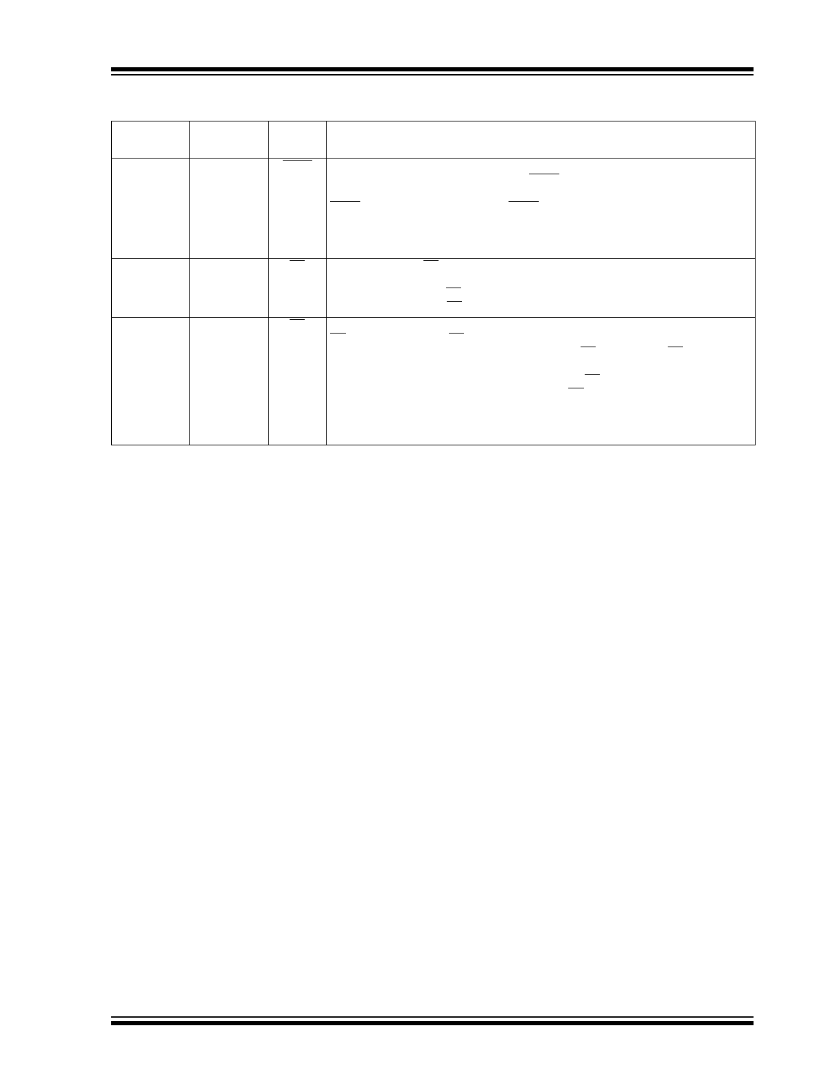
FIGURE 4-1:
TC520 initialization & startup conversion timing relatioNships
FIGURE 4-2:
lOad value modify cycle
4.4.6
OPTO-ISOLATED APPLICATIONS
The 3 wire serial port of the TC520A can be opto-
isolated for applications requiring isolated data acquisi-
tion. The additional control lines (LOAD, DV, READ)
are normally not needed in such applications, but can
also be brought across the isolation barrier with the
addition of a second isolator.
LOAD
LOAD VALUE updated
and conversion started
TC520A Conversion State
CE is pulled
high only during
AZ (DV = Low)
New LOAD VALUE
can be loaded
(if so desired)
TC520A held in
AZ phase
as long as CE = HIGH
CE
AZ
INT
IZ
DINT
AZ
INT
INT
DINT
IZ
AZ
AZ
D
IN
, D
CLK
DV
LOAD VALUE
shifted into
DIN
Load
Value
LOAD
LOAD VALUE updated
and conversion started
TC520A Conversion State
CE
AZ
INT
IZ
DINT
AZ
INT
INT
DINT
IZ
AZ
D
IN
, D
CLK
DV
LOAD VALUE
shift into
D
IN
2001-2012 Microchip Technology Inc.
DS21431C-page 9
TC520A
FIGURE 4-3:
Typical System Application
FIGURE 4-4:
TC520A timing diagram
INT
CAZ
BUF
IN+
IN–
REF+
REF–
COM
1
4
3
OSC
OUT
V+
LOAD
READ
D
CLK
D
IN
D
OUT
C
INT
C
AZ
R
INT
1
µF
Analog Ground
.01
µ
.01
µ
11
10
9
8
5
100k
16
OSC
IN
CMPTR
B
A
DV
CE
GND
14
13
12
6
7
15
2
DGND
2
14
13
5
4
Crystal
6
7
3
C
REF
12
8
10
11
9
TC520A
TC500
+5V
SI
V
IN
-
V
IN
+
SO
SK
RD
LD
10k
DV
CE
1
-5V
MCP1525
V+
CMPTR
B
A
CR–
CR+
GND
V
READ
DOUT
T
RD
DCLK
T
RS
LOAD
D
IN
T
LS
D
CLK
T
DLS
Read Timing
Load Timing
Read Format
READ
DOUT
D
CLK
LOAD
D
IN
MSB
D
CLK
READ
LSB
Load Format
OVR POL MSB
LSB
T
PWL
T
PWH
LOAD
D
IN
T
LDL
Load Default Timing
T
LDS
T
DRS
TC520A
DS21431C-page 10
2001-2012 Microchip Technology Inc.
5.0
PACKAGING INFORMATION
5.1
Package Marking Information
Package marking information not available at this time.
5.2
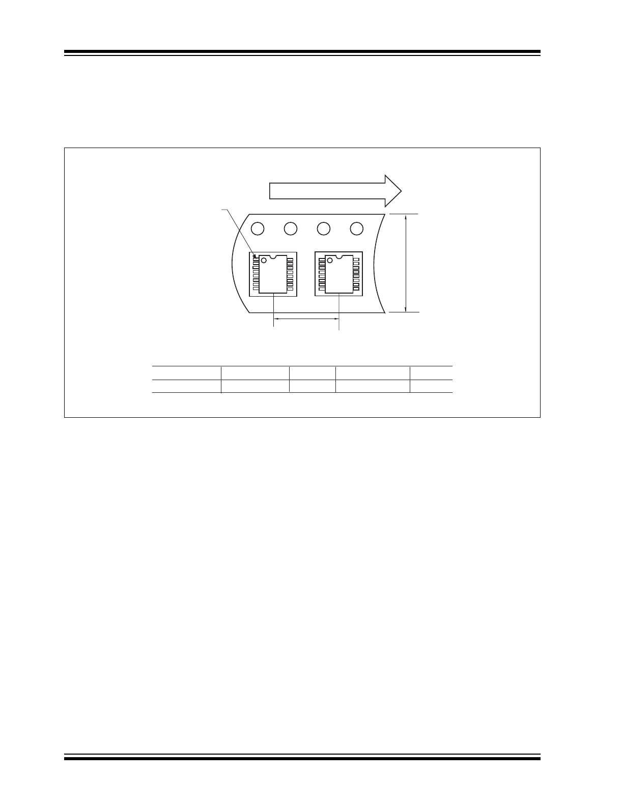
Taping Forms
Component Taping Orientation for 16-Pin SOIC (Wide) Devices
W
PIN 1
User Direction of Feed
Standard Reel Component Orientation
for TR Suffix Device
P
Package
Carrier Width (W)
Pitch (P)
Part Per Full Reel
Reel Size
16-Pin SOIC (W)
16 mm
12 mm
1000
13 in
Carrier Tape, Number of Components Per Reel and Reel Size