
2001-2012 Microchip Technology Inc.
DS21425C-page 1
TC4467/TC4468/TC4469
Features
• High Peak Output Current: 1.2 A
• Wide Operating Range:
- 4.5 V to 18 V
• Symmetrical Rise/Fall Times: 25 nsec
• Short, Equal Delay Times: 75 nsec
• Latch-proof. Will Withstand 500 mA Inductive
Kickback
• 3 Input Logic Choices:
- AND / NAND / AND + Inv
• ESD Protection on All Pins: 2 kV
Applications
• General Purpose CMOS Logic Buffer
• Driving All Four MOSFETs in an H-Bridge
• Direct Small Motor Driver
• Relay or Peripheral Drivers
• CCD Driver
• Pin-Switching Network Driver
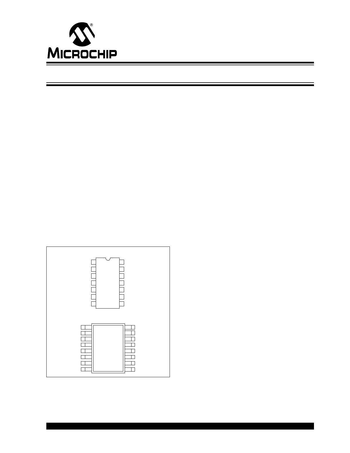
Package Types
General Description
The TC4467/TC4468/TC4469 devices are a family of
four-output CMOS buffers/MOSFET drivers with 1.2 A
peak drive capability. Unlike other MOSFET drivers,
these devices have two inputs for each output. The
inputs are configured as logic gates: NAND (TC4467),
AND (TC4468) and AND/INV (TC4469).
The TC4467/TC4468/TC4469 drivers can continuously
source up to 250 mA into ground referenced loads.
These devices are ideal for direct driving low current
motors or driving MOSFETs in a H-bridge configuration
for higher current motor drive (see Section 5.0 for
details). Having the logic gates onboard the driver can
help to reduce component count in many designs.
The TC4467/TC4468/TC4469 devices are very robust
and highly latch-up resistant. They can tolerate up to
5 V of noise spiking on the ground line and can handle
up to 0.5 A of reverse current on the driver outputs.
The TC4467/4468/4469 devices are available in
commercial, industrial and military temperature ranges.
1
2
3
4
5
6
7
8
16
13
12
11
10
9
1A
1B
2A
2B
3A
3B
GND
GND
V
DD
1Y
2Y
3Y
4Y
4B
4A
V
DD
15
14
TC4467
TC4468
TC4469
16-Pin SOIC (Wide)
1
2
3
4
5
6
7
14
13
12
11
10
9
8
1A
1B
2A
2B
3A
3B
GND
V
DD
1Y
2Y
3Y
4Y
4B
4A
TC4467
TC4468
TC4469
14-Pin PDIP/CERDIP
Logic-Input CMOS Quad Drivers
TC4467/TC4468/TC4469
DS21425C-page 2
2001-2012 Microchip Technology Inc.
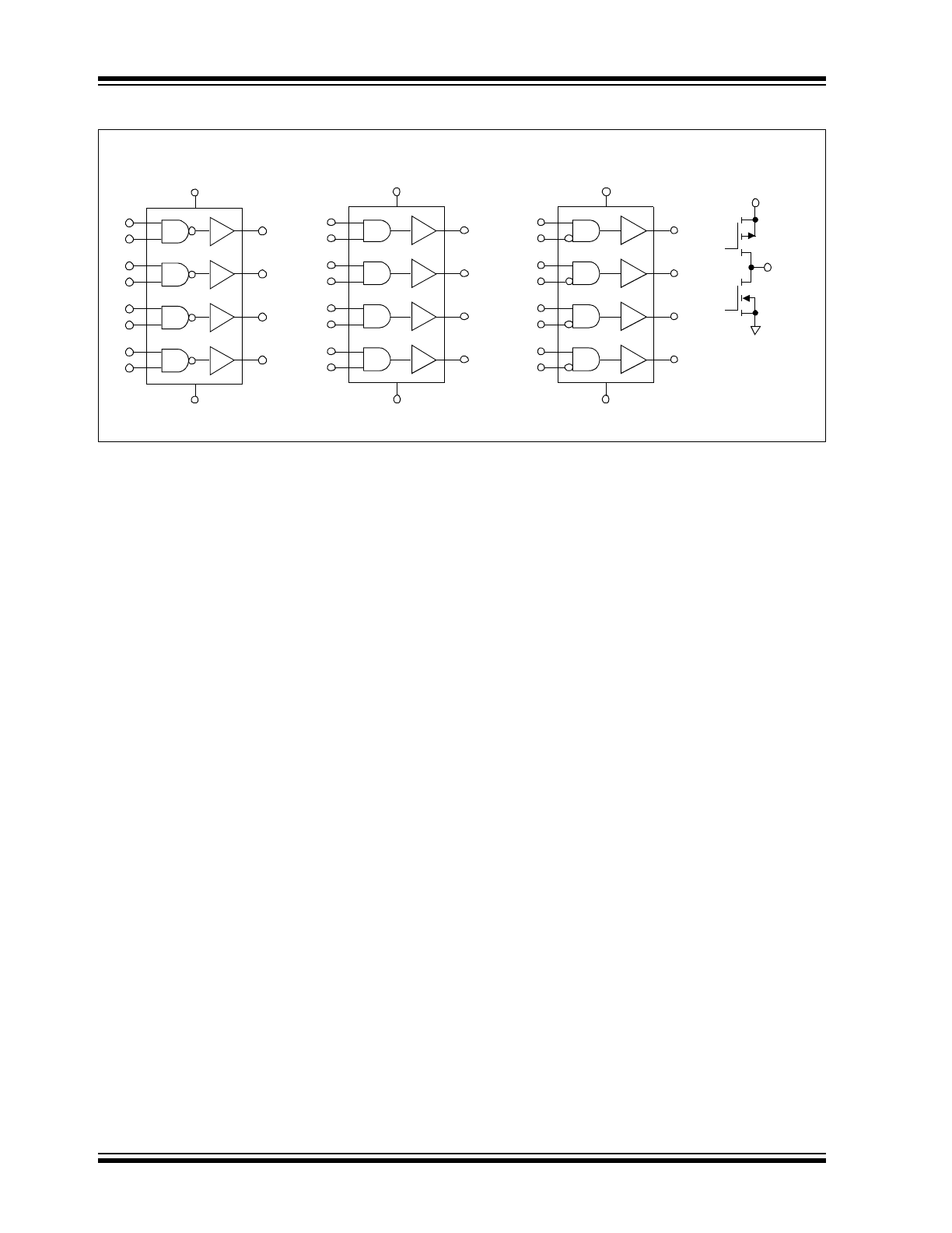
Logic Diagrams
TC4468
TC4467
Output
TC446X
V
DD
14
7
1Y
13
1
2
1B
1A
2Y
12
3
4
2B
2A
3Y
11
5
6
3B
3A
4Y
10
8
9
4B
4A
GND
TC4469
14
7
1Y
13
1
2
1B
1A
2Y
12
3
4
2B
2A
3Y
11
5
6
3B
3A
4Y
10
8
9
4B
4A
14
7
1Y
13
1
2
1B
1A
2Y
12
3
4
2B
2A
3Y
11
5
6
3B
3A
4Y
10
8
9
4B
4A
GND
V
DD
V
DD
V
DD
6
GND
2001-2012 Microchip Technology Inc.
DS21425C-page 3
TC4467/TC4468/TC4469
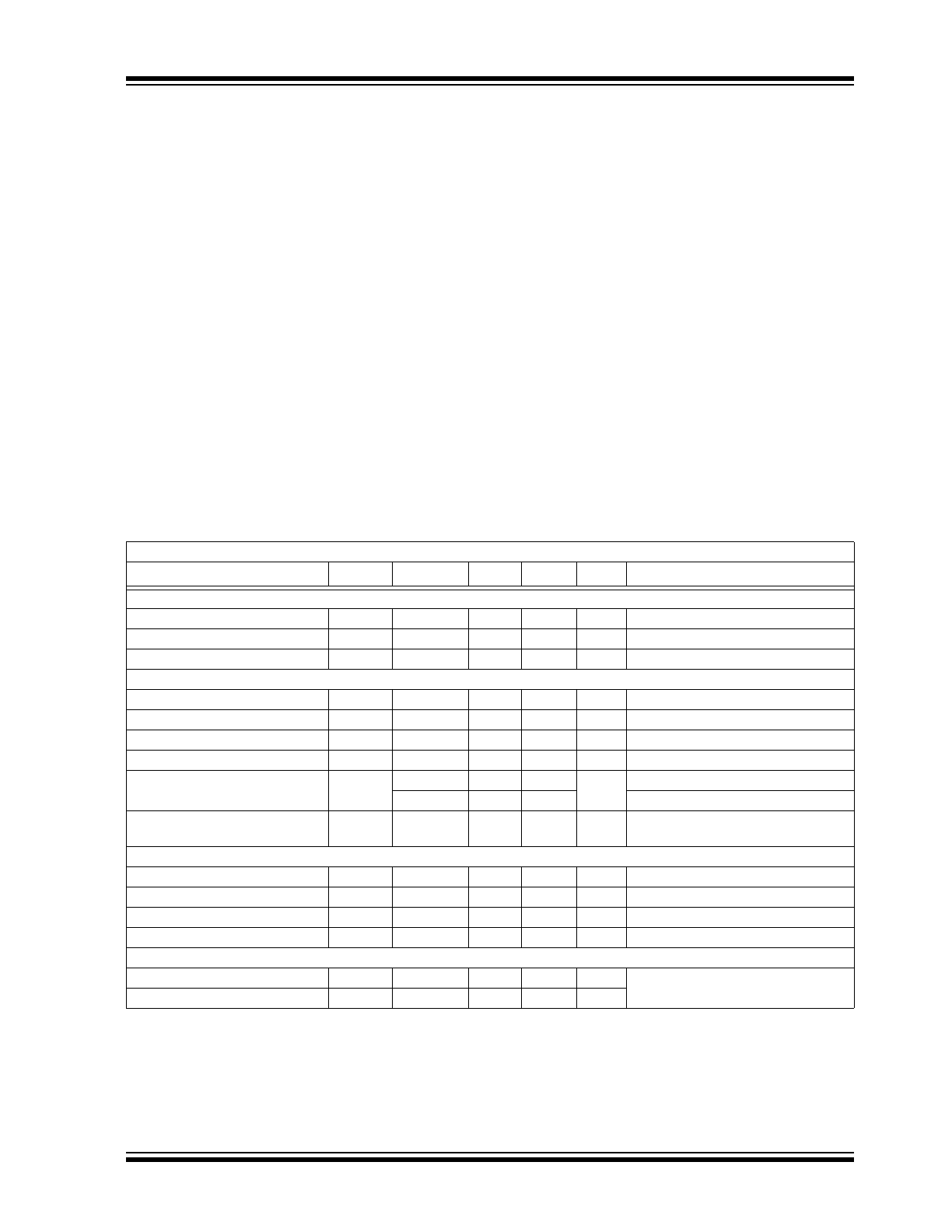
1.0
ELECTRICAL
CHARACTERISTICS
Absolute Maximum Ratings†
Supply Voltage ...............................................................+20 V
Input Voltage ............................. (GND – 5 V) to (V
DD
+ 0.3 V)
Package Power Dissipation: (T
A
70°C)
PDIP...................................................................800 mW
CERDIP .............................................................840 mW
SOIC ..................................................................760 mW
Package Thermal Resistance:
CERDIP R
J-A
...................................................100°C/W
CERDIP R
J-C
.....................................................23°C/W
PDIP R
J-A
..........................................................80°C/W
PDIP R
J-C
..........................................................35°C/W
SOIC R
J-A
..........................................................95°C/W
SOIC R
J-C
..........................................................28°C/W
Operating Temperature Range:
C Version ................................................... 0°C to +70°C
E Version.................................................-40°C to +85°C
M Version ..............................................-55°C to +125°C
Maximum Chip Temperature ....................................... +150°C
Storage Temperature Range .........................-65°C to +150°C
†Notice: Stresses above those listed under "Maximum
Ratings" may cause permanent damage to the device. This is
a stress rating only and functional operation of the device at
those or any other conditions above those indicated in the
operation listings of this specification is not implied. Exposure
to maximum rating conditions for extended periods may affect
device reliability.
ELECTRICAL SPECIFICATIONS
Electrical Characteristics: Unless otherwise noted, T
A
= +25°C, with 4.5 V
V
DD
18 V.
Parameters
Sym
Min
Typ
Max
Units
Conditions
Input
Logic 1, High Input Voltage
V
IH
2.4
—
V
DD
V
Note 3
Logic 0, Low Input Voltage
V
IL
—
—
0.8
V
Note 3
Input Current
I
IN
-1.0
—
+1.0
µA
0 V
V
IN
V
DD
Output
High Output Voltage
V
OH
V
DD
– 0.025
—
—
V
I
LOAD
= 100 µA (Note 1)
Low Output Voltage
V
OL
—
—
0.15
V
I
LOAD
= 10 mA (Note 1)
Output Resistance
R
O
—
10
15
I
OUT
= 10 mA, V
DD
= 18 V
Peak Output Current
I
PK
—
1.2
—
A
Continuous Output Current
I
DC
—
—
300
mA
Single Output
—
—
500
Total Package
Latch-Up Protection Withstand
Reverse Current
I
—
500
—
mA
4.5 V
V
DD
16 V
Switching Time (Note 1)
Rise Time
t
R
—
15
25
nsec
Figure 4-1
Fall Time
t
F
—
15
25
nsec
Figure 4-1
Delay Time
t
D1
—
40
75
nsec
Figure 4-1
Delay Time
t
D2
—
40
75
nsec
Figure 4-1
Power Supply
Power Supply Current
I
S
—
1.5
4
mA
Power Supply Voltage
V
DD
4.5
—
18
V
Note 2
Note
1:
Totem pole outputs should not be paralleled because the propagation delay differences from one to the other could cause one driver to
drive high a few nanoseconds before another. The resulting current spike, although short, may decrease the life of the device. Switching
times are ensured by design.
2:
When driving all four outputs simultaneously in the same direction, V
DD
will be limited to 16 V. This reduces the chance that internal dv/dt
will cause high-power dissipation in the device.
3:
The input threshold has approximately 50 mV of hysteresis centered at approximately 1.5 V. Input rise times should be kept below 5 µsec
to avoid high internal peak currents during input transitions. Static input levels should also be maintained above the maximum, or below
the minimum, input levels specified in the "Electrical Characteristics" to avoid increased power dissipation in the device.
TC4467/TC4468/TC4469
DS21425C-page 4
2001-2012 Microchip Technology Inc.
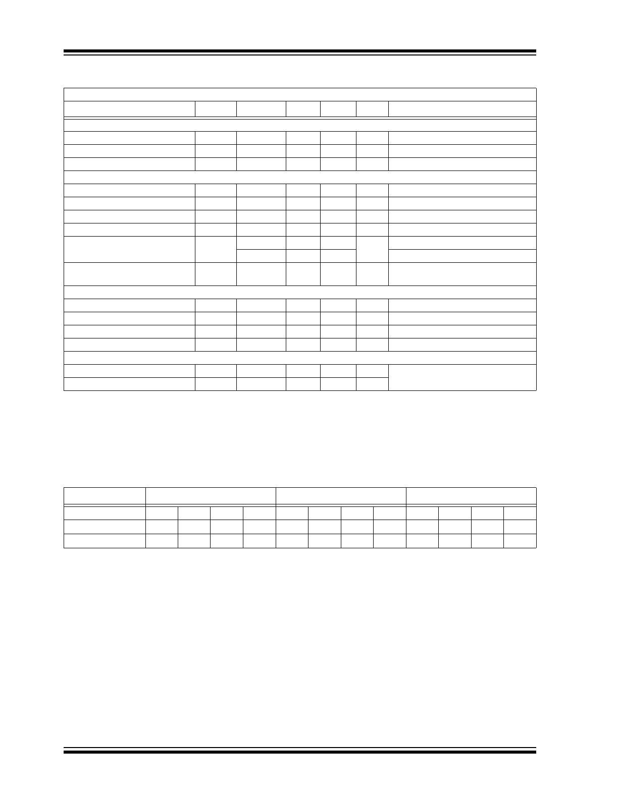
ELECTRICAL SPECIFICATIONS (OPERATING TEMPERATURES)
TRUTH TABLE
Electrical Characteristics: Unless otherwise noted, over operating temperature range with 4.5 V
V
DD
18 V.
Parameters
Sym
Min
Typ
Max
Units
Conditions
Input
Logic 1, High Input Voltage
V
IH
2.4
—
—
V
Note 3
Logic 0, Low Input Voltage
V
IL
—
—
0.8
V
Note 3
Input Current
I
IN
-10
—
10
µA
0 V
V
IN
V
DD
Output
High Output Voltage
V
OH
V
DD
– 0.025
—
—
V
I
LOAD
= 100 µA (Note 1)
Low Output Voltage
V
OL
—
—
0.30
V
I
LOAD
= 10 mA (Note 1)
Output Resistance
R
O
—
20
30
I
OUT
= 10 mA, V
DD
= 18 V
Peak Output Current
I
PK
—
1.2
—
A
Continuous Output Current
I
DC
—
—
300
mA
Single Output
—
—
500
Total Package
Latch-Up Protection Withstand
Reverse Current
I
—
500
—
mA
4.5 V
V
DD
16 V
Switching Time (Note 1)
Rise Time
t
R
—
15
50
nsec
Figure 4-1
Fall Time
t
F
—
15
50
nsec
Figure 4-1
Delay Time
t
D1
—
40
100
nsec
Figure 4-1
Delay Time
t
D2
—
40
100
nsec
Figure 4-1
Power Supply
Power Supply Current
I
S
—
—
8
mA
Power Supply Voltage
V
DD
4.5
—
18
V
Note 2
Note
1:
Totem pole outputs should not be paralleled because the propagation delay differences from one to the other could cause one driver to
drive high a few nanoseconds before another. The resulting current spike, although short, may decrease the life of the device. Switching
times are ensured by design.
2:
When driving all four outputs simultaneously in the same direction, V
DD
will be limited to 16 V. This reduces the chance that internal dv/dt
will cause high-power dissipation in the device.
3:
The input threshold has approximately 50 mV of hysteresis centered at approximately 1.5 V. Input rise times should be kept below 5 µsec
to avoid high internal peak currents during input transitions. Static input levels should also be maintained above the maximum, or below
the minimum, input levels specified in the "Electrical Characteristics" to avoid increased power dissipation in the device.
Part No.
TC4467 NAND
TC4468 AND
TC4469 AND/INV
Inputs A
H
H
L
L
H
H
L
L
H
H
L
L
Inputs B
H
L
H
L
H
L
H
L
H
L
H
L
Outputs TC446X
L
H
H
H
H
L
L
L
L
H
L
L
Legend: H = High
L = Low
2001-2012 Microchip Technology Inc.
DS21425C-page 5
TC4467/TC4468/TC4469
2.0
TYPICAL PERFORMANCE CURVES
Note:
T
A
= +25°C, with 4.5 V
V
DD
18 V.
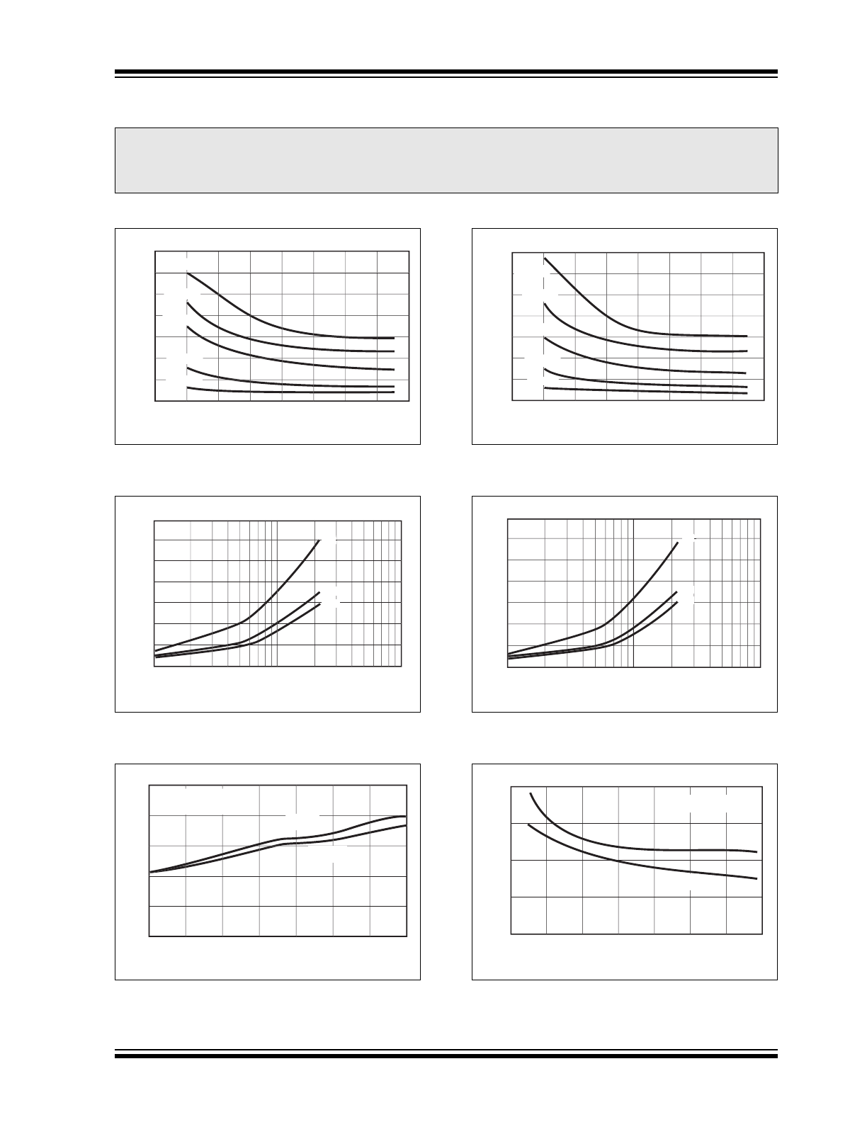
FIGURE 2-1:
Rise Time vs. Supply
Voltage.
FIGURE 2-2:
Rise Time vs. Capacitive
Load.
FIGURE 2-3:
Rise/Fall Times vs.
Temperature.
FIGURE 2-4:
Fall Time vs. Supply
Voltage.
FIGURE 2-5:
Fall Time vs. Capacitive
Load.
FIGURE 2-6:
Propagation Delay Time vs.
Supply Voltage.
Note:
The graphs and tables provided following this note are a statistical summary based on a limited number of
samples and are provided for informational purposes only. The performance characteristics listed herein are
not tested or guaranteed. In some graphs or tables, the data presented may be outside the specified
operating range (e.g., outside specified power supply range) and therefore outside the warranted range.
140
120
100
80
60
40
20
0
3
5
7
9
11
13
15
17
19
2200 pF
0 p
p
1600 pF
1000 pF
470 pF
100 pF
t
R
IS
E
(nsec
)
V
SUPPLY
(V)
140
120
100
80
60
40
20
0
100
1000
10,000
10 V
15 V
V
V
V
5 V
t
R
IS
E
(nsec
)
C
LOAD
(pF)
0
-50
TIME
(nsec
)
5
10
15
20
25
-25
0
25
50
75
100
125
t
FALL
t
RISE
V
SUPPLY
= 17.5 V
C
LOAD
= 470 pF
TEMPERATURE (
°
C)
140
120
100
80
60
40
20
0
3
5
7
9
11
13
15
17
19
p
100 pF
470 pF
1000 pF
1500 pF
2200 pF
t
FALL
(nsec
)
V
SUPPLY
(V)
140
120
100
80
60
40
20
0
100
0
0
1000
10,000
V
V
V
5 V
10 V
15 V
t
FALL
(nsec
)
C
LOAD
(pF)
0
4
D
ELAY TIME
(nsec
)
20
40
60
80
8
12
14
16
18
6
10
V
SUPPLY
(V)
tt
D1
t
D2
C
C
LOAD
470 pF
= 4
TC4467/TC4468/TC4469
DS21425C-page 6
2001-2012 Microchip Technology Inc.
2.0
TYPICAL PERFORMANCE CURVES (CONTINUED)
Note:
T
A
= +25°C, with 4.5 V
V
DD
18 V.
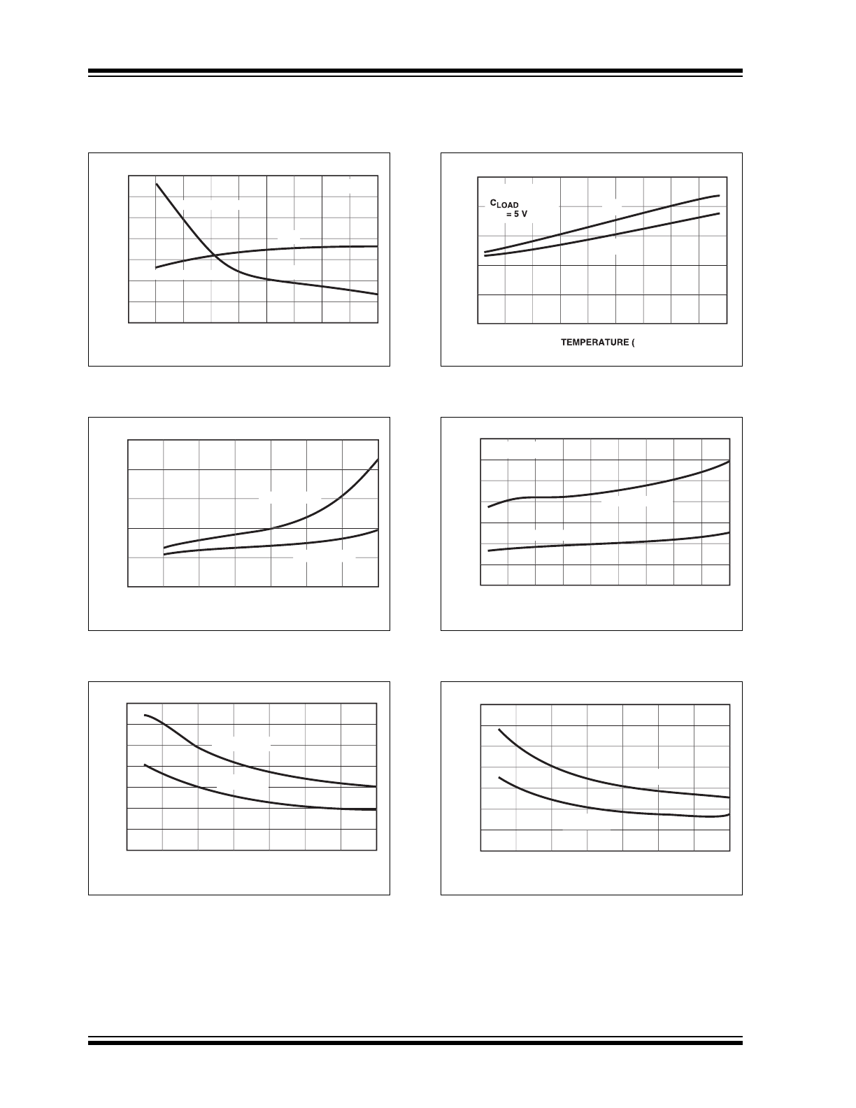
FIGURE 2-7:
Input Amplitude vs. Delay
Times.
FIGURE 2-8:
Quiescent Supply Current
vs. Supply Voltage.
FIGURE 2-9:
High-State Output
Resistance.
FIGURE 2-10:
Propagation Delay Times
vs. Temperatures.
FIGURE 2-11:
Quiescent Supply Current
vs. Temperature.
FIGURE 2-12:
Low-State Output
Resistance.
140
120
100
80
60
40
20
0
1
9
10
D
ELAY TIME
(nsec
)
2
3
4
5
6
7
8
INPUT FALLING
INPUT RISING
V
DRIVE
(V)
t
D1
t
D2
V
DD
V
= 12 V
0
4
0.5
1.0
1.5
2.0
2.5
6
8
10
12
14
16
18
OUTPUTS = 1
OUTPUTS = 0
V
SUPPLY
(V)
I
Q
UIESCENT
(mA
)
0
4
6
8
10
12
14
16
18
V
SUPPLY
(V)
5
10
15
20
25
30
35
R
D
S
(ON
)
(
Ω
)
T
J
= +150
°
C
T
J
= +25
°
C
70
20
100
120
D
ELAY TIME
(nsec
)
-40
-20
0
20
40
60
80
30
40
50
60
-60
°
C)
V
DD
= 17.5 V
= 470 pF
V
IN
t
D1
t
D2
3.5
0
100
120
-40
-20
0
20
40
60
80
3.0
2.5
2.0
1.5
1.0
0.5
OUTPUTS = 1
OUTPUTS = 0
-60
I
Q
UIESCENT
(mA)
T
JUNCTION
(
°
C)
V
V
DD
= 17.5 V
0
4
6
8
10
12
14
16
18
5
10
15
20
25
30
35
V
SUPPLY
(V)
R
D
S
(ON
)
(
Ω
)
T
J
= +150
°
C
T
J
= +25
°
C
2001-2012 Microchip Technology Inc.
DS21425C-page 7
TC4467/TC4468/TC4469
2.0
TYPICAL PERFORMANCE CURVES (CONTINUED)
Note:
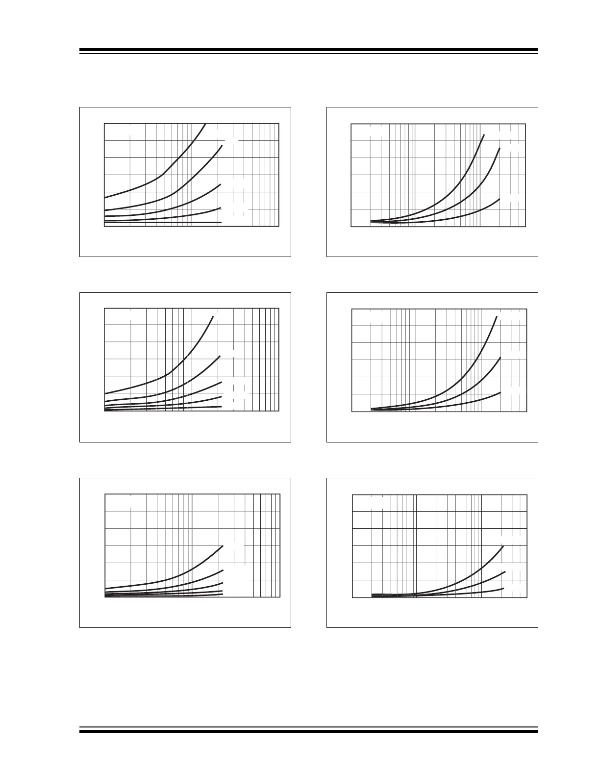
(Load on single output only).
FIGURE 2-13:
Supply Current vs.
Capacitive Load.
FIGURE 2-14:
Supply Current vs.
Capacitive Load.
FIGURE 2-15:
Supply Current vs.
Capacitive Load.
FIGURE 2-16:
Supply Current vs.
Frequency.
FIGURE 2-17:
Supply Current vs.
Frequency.
FIGURE 2-18:
Supply Current vs.
Frequency.
60
0
100
1000
10,000
50
40
30
20
10
2 MH
Hz
1 MHz
1 MHz
1 MH
50
00 kHz
200 kHz
20 kHz
I
SU
PPL
Y
(mA
)
C
LOAD
(pF)
V
DD
= 18 V
60
0
100
1000
10,000
50
40
30
20
10
2 MHz
2 MHz
1 MHz
500 kHz
200 kHz
20 kHz
C
LOAD
(pF)
I
SU
PPLY
(mA
)
V
DD
V
= 12 V
60
50
40
30
20
10
0
100
1000
10,000
1 MHz
500 kHz
200 kHz
20 kHz
2 MHz
I
SU
PPLY
(mA
)
C
LOAD
(pF)
V
V
DD
V
= 6 V
60
0
100
1000
FREQUENCY (kHz)
50
40
30
20
10
2200 pF
1
1000 pF
p
100 pF
10
10,000
V
DD
= 18 V
I
SU
PPLY
(mA
)
60
0
10
100
FREQUENCY (kHz)
50
40
30
20
10
1000
2200 pF
p
p
1000 pF
100 pF
10,000
I
SU
PPLY
(mA
)
V
DD
V
= 12 V
60
0
10
1000
100
FREQUENCY (kHz)
50
40
30
20
10
2200 pF
1000 pF
100 pF
10,000
I
SU
PPLY
(mA
)
V
V
DD
= 6 V
TC4467/TC4468/TC4469
DS21425C-page 8
2001-2012 Microchip Technology Inc.
3.0
PIN DESCRIPTIONS
The descriptions of the pins are listed in Table 3-1.
TABLE 3-1:
PIN FUNCTION TABLE
14-Pin PDIP,
CERDIP
16-Pin SOIC
(Wide)
Description
Symbol
Symbol
1A
1A
Input A for Driver 1, TTL/CMOS Compatible Input
1B
1B
Input B for Driver 1, TTL/CMOS Compatible Input
2A
2A
Input A for Driver 2, TTL/CMOS Compatible Input
2B
2B
Input B for Driver 2, TTL/CMOS Compatible Input
3A
3A
Input A for Driver 3, TTL/CMOS Compatible Input
3B
3B
Input B for Driver 3, TTL/CMOS Compatible Input
GND
GND
Ground
—
GND
Ground
4A
4A
Input A for Driver 4, TTL/CMOS Compatible Input
4B
4B
Input B for Driver 4, TTL/CMOS Compatible Input
4Y
4Y
Output for Driver 4, CMOS Push-Pull Output
3Y
3Y
Output for Driver 3, CMOS Push-Pull Output
2Y
2Y
Output for Driver 2, CMOS Push-Pull Output
1Y
1Y
Output for Driver 1, CMOS Push-Pull Output
V
DD
V
DD
Supply Input, 4.5 V to 18 V
—
V
DD
Supply Input, 4.5 V to 18 V

2001-2012 Microchip Technology Inc.
DS21425C-page 9
TC4467/TC4468/TC4469
4.0
DETAILED DESCRIPTION
4.1
Supply Bypassing
Large currents are required to charge and discharge
large capacitive loads quickly. For example, charging a
1000 pF load to 18 V in 25 nsec requires 0.72 A from
the device's power supply.
To ensure low supply impedance over a wide frequency
range, a 1 µF film capacitor in parallel with one or two
low-inductance, 0.1 µF ceramic disk capacitors with
short lead lengths (<0.5 in.) normally provide adequate
bypassing.
4.2
Grounding
The TC4467 and TC4469 contain inverting drivers.
Potential drops developed in common ground
impedances from input to output will appear as
negative feedback and degrade switching speed
characteristics. Instead, individual ground returns for
input and output circuits, or a ground plane, should be
used.
4.3
Input Stage
The input voltage level changes the no-load or
quiescent supply current. The N-channel MOSFET
input stage transistor drives a 2.5 mA current source
load. With logic “0” outputs, maximum quiescent supply
current is 4 mA. Logic “1” output level signals reduce
quiescent current to 1.4 mA, maximum. Unused driver
inputs must be connected to V
DD
or V
SS
. Minimum
power dissipation occurs for logic “1” outputs.
The drivers are designed with 50 mV of hysteresis,
which provides clean transitions and minimizes output
stage current spiking when changing states. Input volt-
age thresholds are approximately 1.5 V, making any
voltage greater than 1.5 V, up to V
DD
,
a logic “1” input.
Input current is less than 1 µA over this range.
4.4
Power Dissipation
The supply current versus frequency and supply
current versus capacitive load characteristic curves will
aid in determining power dissipation calculations.
Microchip Technology's CMOS drivers have greatly
reduced quiescent DC power consumption.
Input signal duty cycle, power supply voltage and load
type influence package power dissipation. Given power
dissipation and package thermal resistance, the maxi-
mum ambient operating temperature is easily
calculated. The 14-pin plastic package junction-to-
ambient thermal resistance is 83.3°C/W. At +70°C, the
package is rated at 800 mW maximum dissipation.
Maximum allowable chip temperature is +150°C.
Three components make up total package power
dissipation:
1.
Load-caused dissipation (P
L
).
2.
Quiescent power (P
Q
).
3.
Transition power (P
T
).
A capacitive-load-caused dissipation (driving MOSFET
gates), is a direct function of frequency, capacitive load
and supply voltage. The power dissipation is:
EQUATION
A resistive-load-caused dissipation for ground-
referenced loads is a function of duty cycle, load
current and load voltage. The power dissipation is:
EQUATION
P
L
fCV
S
2
=
V
S
Supply Voltage
=
C
Capacitive Load
=
f
Switching Frequency
=
P
L
D V
S
V
L
–
I
L
=
I
L
Load Current
=
D
Duty Cycle
=
V
S
Supply Voltage
=
V
L
Load Voltage
=
TC4467/TC4468/TC4469
DS21425C-page 10
2001-2012 Microchip Technology Inc.
A resistive-load-caused dissipation for supply-
referenced loads is a function of duty cycle, load
current and output voltage. The power dissipation is
EQUATION
Quiescent power dissipation depends on input signal
duty cycle. Logic HIGH outputs result in a lower power
dissipation mode, with only 0.6 mA total current drain
(all devices driven). Logic LOW outputs raise the
current to 4 mA maximum. The quiescent power
dissipation is:
EQUATION
Transition power dissipation arises in the complimen-
tary configuration (TC446X) because the output stage
N-channel and P-channel MOS transistors are ON
simultaneously for a very short period when the output
changes. The transition power dissipation is
approximately:
EQUATION
Package power dissipation is the sum of load,
quiescent and transition power dissipations. An
example shows the relative magnitude for each term:
Maximum operating temperature is:
EQUATION
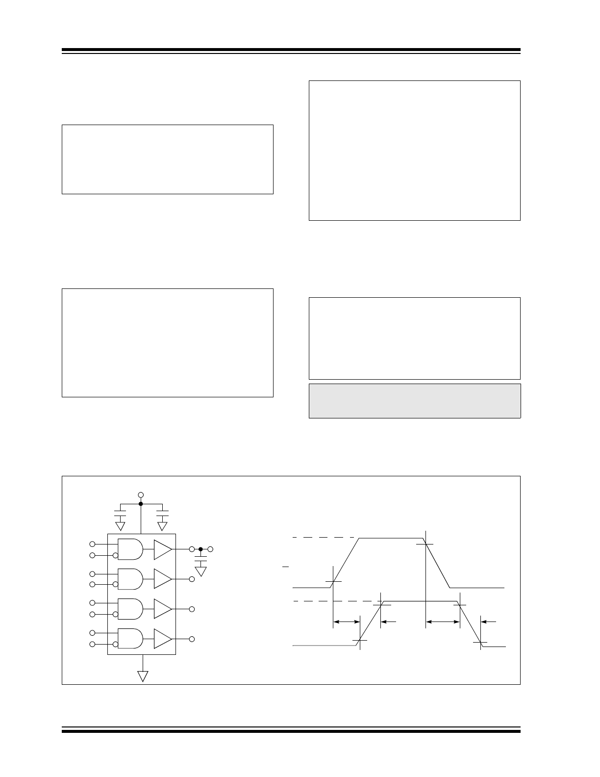
FIGURE 4-1:
Switching Time Test Circuit.
P
L
DV
O
I
L
=
I
L
Load Current
=
V
O
Device Output Voltage
=
D
Duty Cycle
=
P
Q
V
S
D I
H
1
D
–
I
L
+
=
I
L
Quiescent Current with all outputs HIGH
=
I
H
Quiescent Current with all outputs LOW
=
D
Duty Cycle
=
V
S
Supply Voltage
=
(4 mA max.)
(0.6 mA max.)
Note:
Ambient operating temperature should not
exceed +85°C for "EJD" device or +125°C
for "MJD" device.
P
T
fV
s
10
10
9
–
=
V
S
15 V
=
C
1000 pF Capacitive Load
=
D
50%
=
f
200 kHz
=
P
D
Package Power Dissipation
=
P
L
P
Q
P
T
+
+
=
45mW
35mW
30mW
+
+
=
110mW
=
T
J
J A
P
D
–
141
C
=
JA
Junction-to-ambient thernal resistance
=
T
J
Maximum allowable junction temperature
=
(+150
C
(83.3
C/W) 14-pin plastic package
V
OUT
470 pF
1B
1A
2B
2A
3B
3A
4B
4A
1 µF Film
0.1 µF Ceramic
90%
10%
10%
10%
90%
+5 V
Input
(A, B)
V
DD
Output
0 V
0V
90%
1
2
3
4
5
6
8
9
7
10
11
12
13
14
V
DD
t
R
t
D1
t
F
t
D2
Input: 100 kHz,
square wave,
t
RISE
= t
FALL
10 nsec