
2002-2012 Microchip Technology Inc.
DS21416D-page 1
TC429
Features
• High Peak Output Current: 6A
• Wide Input Supply Voltage Operating Range:
- 7V to 18V
• High-Impedance CMOS Logic Input
• Logic Input Threshold Independent of Supply
Voltage
• Low Supply Current:
- With Logic ‘1’ Input – 5 mA max.
- With Logic ‘0’ Input – 0.5 mA max.
• Output Voltage Swing Within 25 mV of Ground
or V
DD
• Short Delay Time: 75 nsec max
• Available in the Space-Saving 8-Pin SOIC
Package.
• High Capacitive Load Drive Capability:
- t
RISE
, t
FALL
= 35 nsec max with
C
LOAD
= 2500 pF
Applications
• Switch-Mode Power Supplies
• CCD Drivers
• Pulse Transformer Drive
• Class D Switching Amplifiers
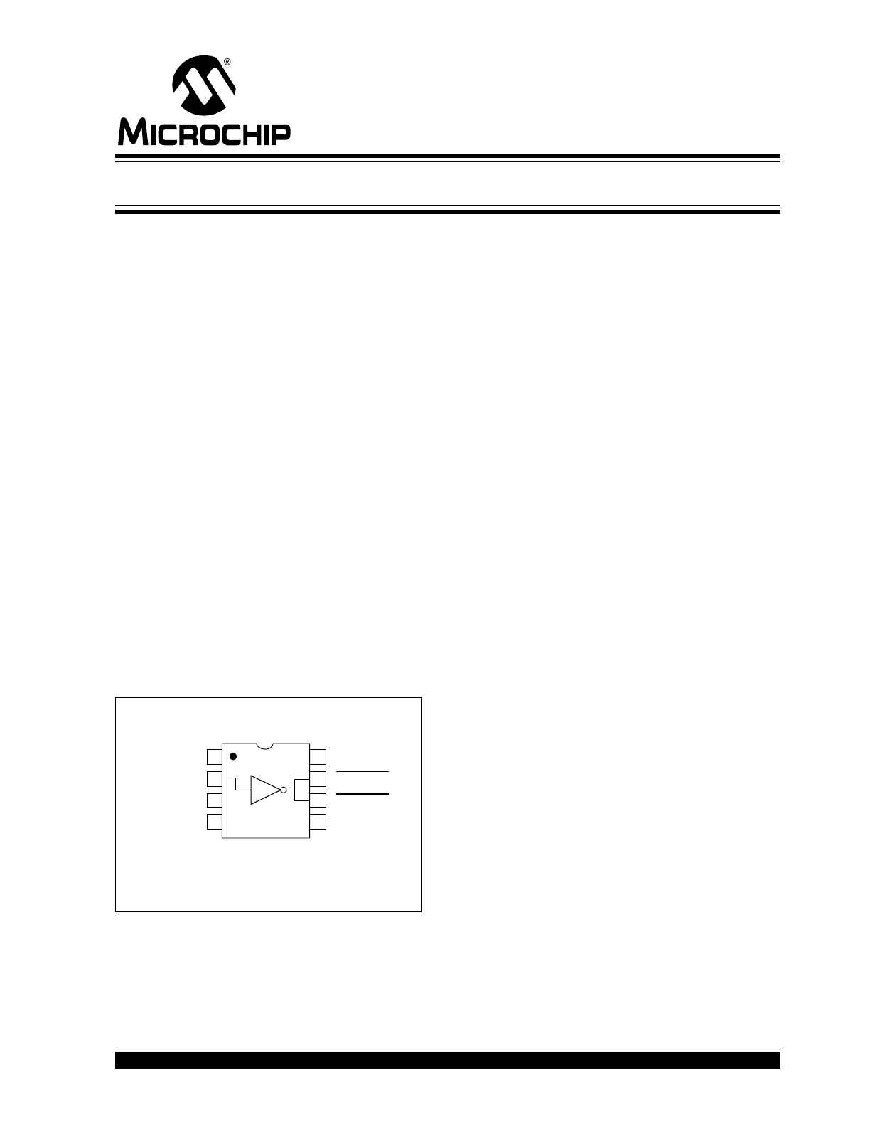
Package Types
General Description
The TC429 is a high-speed, single output, CMOS-level
translator and driver. Designed specifically to drive
highly capacitive power MOSFET gates, the TC429
features a 2.5
output impedance and 6A peak output
current drive.
A 2500 pF capacitive load will be driven to 18V in
25
nsec. The rapid switching times with large
capacitive loads minimize MOSFET switching power
losses.
A TTL/CMOS input logic level is translated into an
output voltage swing that equals the supply voltage and
will swing to within 25 mV of ground or V
DD
. Input volt-
age swing may equal the supply voltage. Logic input
current is under 10 µA, making direct interface to
CMOS/bipolar switch-mode power supply controllers
easy. Input “speed-up” capacitors are not required.
The CMOS design minimizes quiescent power supply
current. With a logic ‘1’ input, power supply current is
5 mA maximum and decreases to 0.5 mA for logic ‘0’
inputs.
For dual output MOSFET drivers, see the TC426/
TC427/TC428 (DS21415), TC4426/TC4427/TC4428
(DS21422) and TC4426A/TC4427A/TC4428A
(DS21423) data sheets.
For non-inverting applications, or applications requiring
latch-up protection, see the TC4420/TC4429
(DS21419) data sheet.
CERDIP/PDIP/SOIC
1
2
3
4
V
DD
5
6
7
8
OUTPUT
GND
V
DD
INPUT
NC
GND
OUTPUT
TC429
NC = No Internal Connection
Note: Duplicate pins must both be connected for
proper operation.
6A Single High-Speed, CMOS Power MOSFET Driver
TC429
DS21416D-page 2
2002-2012 Microchip Technology Inc.
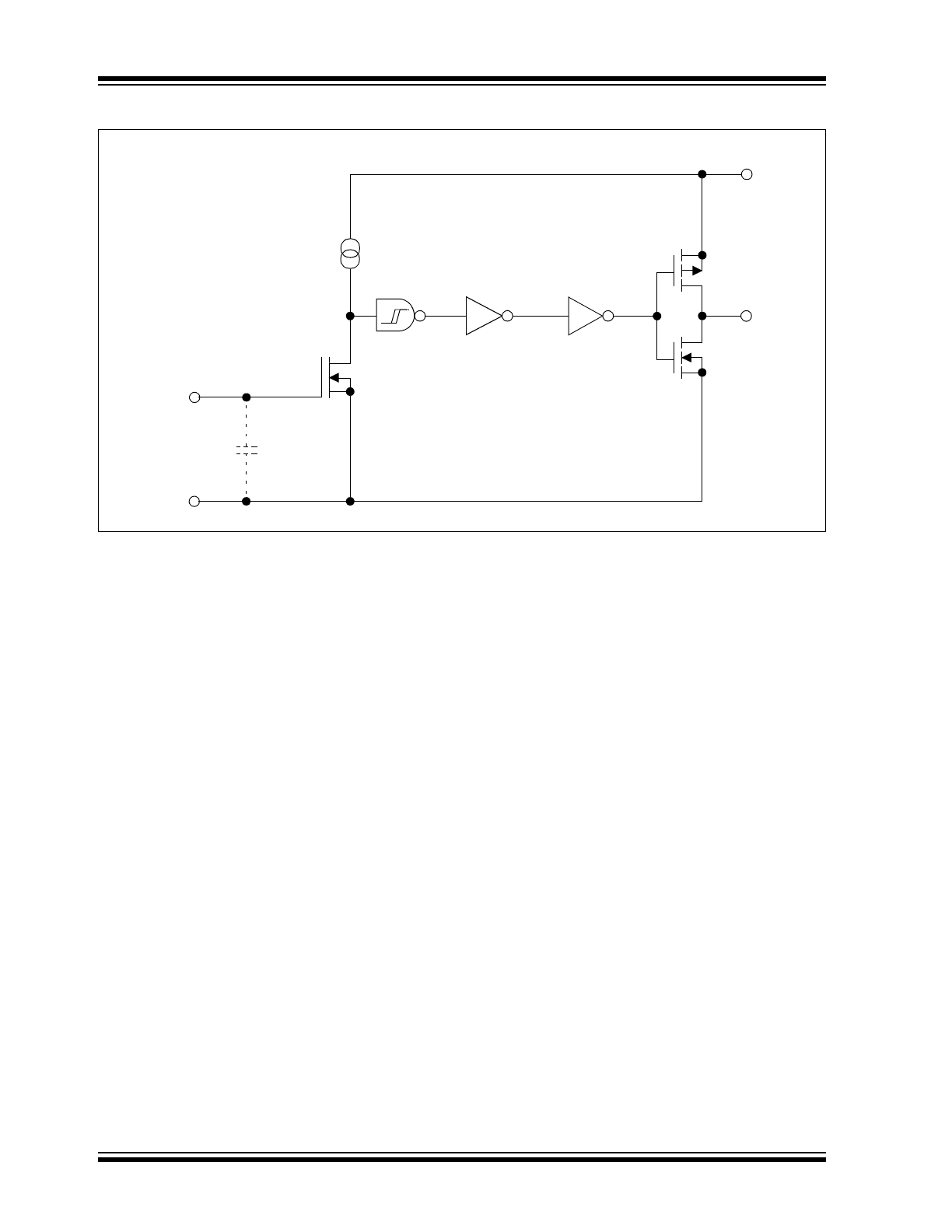
Functional Block Diagram
Effective
Input C = 38 pF
TC429
Output
Input
GND
V
DD
300 mV
1,8
6,7
2
4,5
2002-2012 Microchip Technology Inc.
DS21416D-page 3
TC429
1.0
ELECTRICAL
CHARACTERISTICS
Absolute Maximum Ratings †
Supply Voltage ..................................................... +20V
Input Voltage, Any Terminal
................................... V
DD
+ 0.3V to GND – 0.3V
Power Dissipation (T
A
70°C)
PDIP ............................................................ 730
mW
CERDIP ....................................................... 800
mW
SOIC............................................................ 470
mW
Storage Temperature Range.............. -65°C to +150°C
Maximum Junction Temperature, T
J
............... +150°C
† Stresses above those listed under "Absolute Maximum
Ratings" may cause permanent damage to the device. These
are stress ratings only and functional operation of the device
at these or any other conditions above those indicated in the
operation sections of the specifications is not implied.
Exposure to Absolute Maximum Rating conditions for
extended periods may affect device reliability.
PIN FUNCTION TABLE
DC ELECTRICAL CHARACTERISTICS
Symbol
Description
V
DD
Supply input, 7V to 18V
INPUT
Control input. TTL/CMOS compatible
logic input
NC
No connection
GND
Ground
GND
Ground
OUTPUT
CMOS push-pull, common to pin 7
OUTPUT
CMOS push-pull, common to pin 6
V
DD
Supply input, 7V to 18V
Electrical Specifications: Unless otherwise noted, T
A
= +25°C with 7V
V
DD
18V.
Parameters
Sym
Min
Typ
Max
Units
Conditions
Input
Logic ‘1’, High Input Voltage
V
IH
2.4
1.8
—
V
Logic ‘0’, Low Input Voltage
V
IL
—
1.3
0.8
V
Input Current
I
IN
-10
—
10
µA
0V
V
IN
V
DD
Output
High Output Voltage
V
OH
V
DD
– 0.025
—
—
V
Low Output Voltage
V
OL
—
—
0.025
V
Output Resistance
R
O
—
1.8
2.5
V
IN
= 0.8V,
V
OUT
= 10 mA, V
DD
= 18V
—
1.5
2.5
V
IN
= 2.4V,
V
OUT
= 10 mA, V
DD
= 18V
Peak Output Current
I
PK
—
6.0
—
A
V
DD
= 18V, Figure 4-4
Latch-Up Protection
Withstand Reverse Current
I
REV
—
0.5
—
A
Duty cycle
2%, t 300 µsec,
V
DD
= 16V
Switching Time (Note 1)
Rise Time
t
R
—
23
35
nsec
C
L
= 2500 pF, Figure 4-1
Fall Time
t
F
—
25
35
nsec
C
L
= 2500 pF, Figure 4-1
Delay Time
t
D1
—
53
75
nsec
Figure 4-1
Delay Time
t
D2
—
60
75
nsec
Figure 4-1
Power Supply
Power Supply Current
I
S
—
3.5
5.0
mA
V
IN
= 3V
—
0.3
0.5
V
IN
= 0V
Note 1: Switching times ensured by design.
TC429
DS21416D-page 4
2002-2012 Microchip Technology Inc.
DC ELECTRICAL CHARACTERISTICS (CONTINUED)
TEMPERATURE CHARACTERISTICS
Electrical Specifications: Unless otherwise noted, over operating temperature range with 7V
V
DD
18V.
Parameters
Sym
Min
Typ
Max
Units
Conditions
Input
Logic ‘1’, High Input Voltage
V
IH
2.4
—
—
V
Logic ‘0’, Low Input Voltage
V
IL
—
—
0.8
V
Input Current
I
IN
-10
—
10
µA
0V
V
IN
V
DD
Output
High Output Voltage
V
OH
V
DD
– 0.025
—
—
V
Low Output Voltage
V
OL
—
—
0.025
V
Output Resistance
R
O
—
—
5.0
V
IN
= 0.8V,
V
OUT
= 10 mA, V
DD
= 18V
—
—
5.0
V
IN
= 2.4V,
V
OUT
= 10 mA, V
DD
= 18V
Switching Time (Note 1)
Rise Time
t
R
—
—
70
nsec
C
L
= 2500 pF, Figure 4-1
Fall Time
t
F
—
—
70
nsec
C
L
= 2500 pF, Figure 4-1
Delay Time
t
D1
—
—
100
nsec
Figure 4-1
Delay Time
t
D2
—
—
120
nsec
Figure 4-1
Power Supply
Power Supply Current
I
S
—
—
12
mA
V
IN
= 3V
—
—
1.0
V
IN
= 0V
Note 1: Switching times ensured by design.
Electrical Specifications: Unless otherwise noted, T
A
= +25°C with 7V
V
DD
18V.
Parameters
Sym
Min
Typ
Max
Units
Conditions
Temperature Ranges
Specified Temperature Range (C)
T
A
0
—
+70
ºC
Specified Temperature Range (E)
T
A
-40
—
+85
ºC
Specified Temperature Range (M)
T
A
-55
—
+125
ºC
Maximum Junction Temperature
T
J
—
—
+150
ºC
Storage Temperature Range
T
A
-65
—
+150
ºC
Package Thermal Resistances
Thermal Resistance, 8L-CERDIP
JA
—
150
—
ºC/W
Thermal Resistance, 8L-PDIP
JA
—
125
—
ºC/W
Thermal Resistance, 8L-SOIC
JA
—
155
—
ºC/W
2002-2012 Microchip Technology Inc.
DS21416D-page 5
TC429
2.0
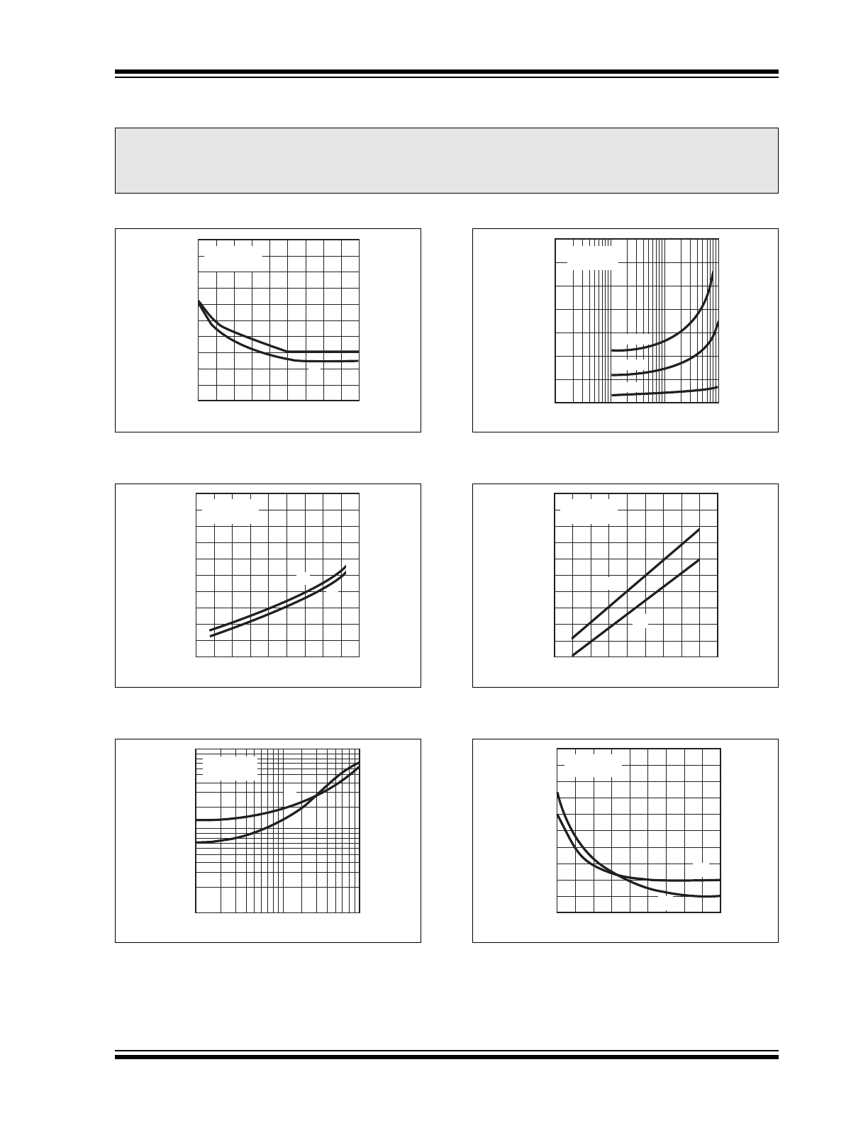
TYPICAL PERFORMANCE CURVES
Note: Unless otherwise indicated, T
A
= +25°C with 7V
V
DD
18V.
FIGURE 2-1:
Rise/Fall Times vs. Supply
Voltage.
FIGURE 2-2:
Rise/Fall Times vs.
Temperature.
FIGURE 2-3:
Rise/Fall Times vs.
Capacitive Load.
FIGURE 2-4:
Supply Current vs.
Capacitive Load.
FIGURE 2-5:
Delay Times vs.
Temperature.
FIGURE 2-6:
Delay Times vs. Supply
Voltage.
Note:
The graphs and tables provided following this note are a statistical summary based on a limited number of
samples and are provided for informational purposes only. The performance characteristics listed herein
are not tested or guaranteed. In some graphs or tables, the data presented may be outside the specified
operating range (e.g., outside specified power supply range) and therefore outside the warranted range.
60
50
40
30
20
10
5
10
15
20
SUPPLY VOLTAGE (V)
TIME (nsec)
T
A
= +25
°C
C
L
= 2500 pF
t
R
t
F
60
50
40
30
20
10
0
75
TEMPERATURE (
°C)
TIME (nsec)
C
L
= 2500 pF
V
DD
= +15V
-50 -25
25 50
100 125 150
t
R
t
F
100
10
1
100
1K
10K
CAPACITIVE LOAD (pF)
TIME (nsec)
t
R
t
F
T
A
= +25
°C
V
DD
= +15V
70
60
50
40
30
20
10
0
SUPPLY CURRENT (mA)
10
100
1K
10K
CAPACITIVE LOAD (pF)
200 kHz
20 kHz
T
A
= +25
°C
V
DD
= +15V
400 kHz
90
80
70
60
50
40
0
75
TEMPERATURE (
°C)
DELAY TIME (nsec)
-50 -25
25 50
100 125
t
D2
t
D1
C
L
= 2500 pF
V
DD
= +15V
150
140
120
100
80
60
40
5
DELAY TIME (nsec)
10
15
20
SUPPLY VOLTAGE (V)
t
D1
t
D2
T
A
= +25
°C
C
L
= 2500 pF
TC429
DS21416D-page 6
2002-2012 Microchip Technology Inc.
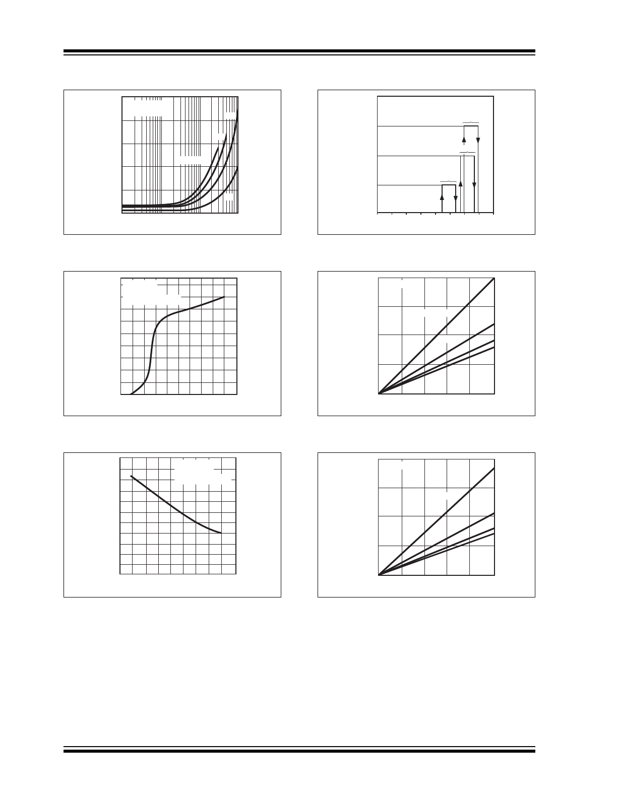
Note: Unless otherwise indicated, T
A
= +25°C with 7V
V
DD
18V.
FIGURE 2-7:
Supply Current vs.
Frequency.
FIGURE 2-8:
Supply Current vs. Supply
Voltage.
FIGURE 2-9:
Supply Current vs.
Temperature.
.
FIGURE 2-10:
Voltage Transfer
Characterstics.
FIGURE 2-11:
High Output Voltage
(V
DD
-V
OH
) vs. Output Source Current.
FIGURE 2-12:
Low Output Voltage vs.
Output Sink Current.
50
40
30
20
10
0
1
10
100
1K
15V
10V
V
DD
= 18V
5V
T
A
= +25
°C
C
L
= 2500 pF
SUPPLY CURRENT (mA)
FREQUENCY (kHz)
4
2
0
4
8
12
16
20
SUPPLY CURRENT (mA)
SUPPLY VOLTAGE (V)
T
A
= +25
°C
R
L
=
∞
INPUT LOGIC "1"
4
3
2
-75
-25
50
100
150
SUPPLY CURRENT (mA)
TEMPERATURE (
°C)
-50
0
25
75
125
V
DD
= +18
°C
R
L
=
∞
INPUT LOGIC "1"
HYSTERESIS
≈310 mV
200 mV
300 mV
20
15
10
5
0
1.25
0.25 0.50 0.75
1
1.50 1.75
2
T
A
= +25
°C
OUTPUT VOLTAGE (V)
INPUT VOLTAGE (V)
OUTPUT VOLTAGE (mV)
400
300
200
100
SOURCE CURRENT (mA)
0
20
40
60
80
100
V
DD
= 5V
10V
15V
18V
T
A
= +25
°C
OUTPUT VOLTAGE (mV)
400
300
200
100
SINK CURRENT (mA)
0
20
40
60
80
100
V
DD
= 5V
10V
15V
18V
T
A
= +25
°C
2002-2012 Microchip Technology Inc.
DS21416D-page 7
TC429
3.0
PIN DESCRIPTIONS
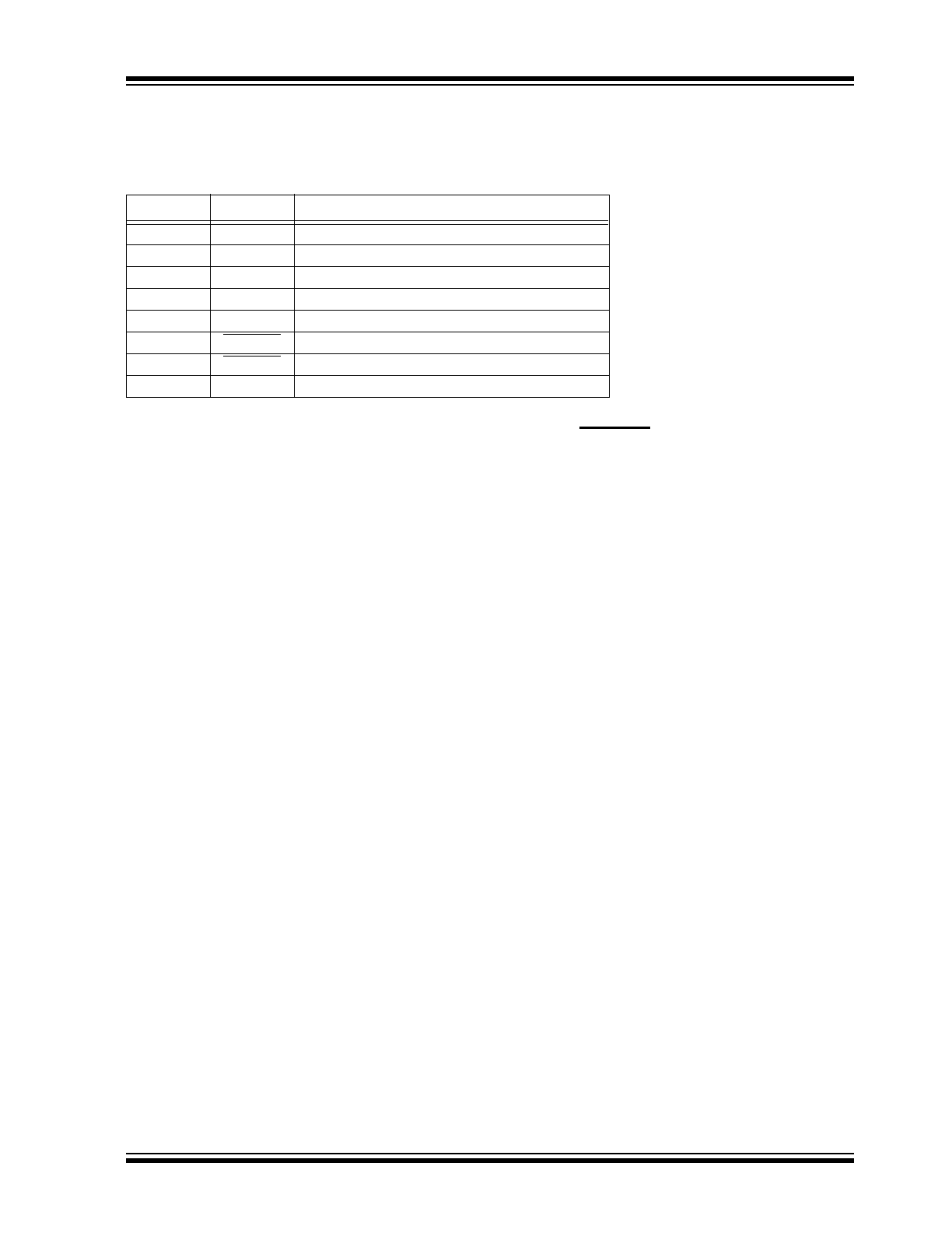
The descriptions of the pins are listed in Table 3-1.
TABLE 3-1:
PIN FUNCTION TABLE
3.1
Supply Input (V
DD
)
The V
DD
input is the bias supply for the MOSFET driver
and is rated for 7.0V to 18V with respect to the ground
pin. The V
DD
input should be bypassed to ground with
a local ceramic capacitor. The value of the capacitor
should be chosen based on the capacitive load that is
being driven. A value of 1.0 µF is suggested.
3.2
Control Input (INPUT)
The MOSFET driver input is a high-impedance,
TTL/CMOS compatible input. The input also has
300 mV of hysteresis between the high and low thresh-
olds that prevents output glitching even when the rise
and fall time of the input signal is very slow.
3.3
CMOS Push-Pull Output
(OUTPUT)
The MOSFET driver output is a low-impedance, CMOS
push-pull style output, capable of driving a capacitive
load with 6.0A peak currents.
3.4
Ground (GND)
The ground pins are the return path for the bias current
and for the high peak currents that discharge the load
capacitor. The ground pins should be tied into a ground
plane or have very short traces to the bias supply
source return.
3.5
No Connect (NC)
No connection.
Pin No.
Symbol
Description
1
V
DD
Supply input, 7V to 18V
2
INPUT
Control input. TTL/CMOS compatible logic input
3
NC
No connection
4
GND
Ground
5
GND
Ground
6
OUTPUT
CMOS push-pull output, common to pin 7
7
OUTPUT
CMOS push-pull output, common to pin 6
8
V
DD
Supply input, 7V to 18V
TC429
DS21416D-page 8
2002-2012 Microchip Technology Inc.
4.0
APPLICATIONS INFORMATION
4.1
Supply Bypassing
Charging and discharging large capacitive loads
quickly requires large currents. For example, charging
a 2500 pF load to 18V in 25 nsec requires a 1.8A
current from the device's power supply.
To ensure low supply impedance over a wide frequency
range, a parallel capacitor combination is recom-
mended for supply bypassing. Low-inductance ceramic
disk capacitors with short lead lengths (< 0.5 in.) should
be used. A 1 µF film capacitor in parallel with one or two
0.1
µF ceramic disk capacitors normally provides
adequate bypassing.
4.2
Grounding
The high-current capability of the TC429 demands
careful PC board layout for best performance. Since
the TC429 is an inverting driver, any ground lead
impedance will appear as negative feedback that can
degrade switching speed. The feedback is especially
noticeable with slow rise-time inputs, such as those
produced by an open-collector output with resistor pull-
up. The TC429 input structure includes about 300 mV
of hysteresis to ensure clean transitions and freedom
from oscillation, but attention to layout is still
recommended.
Figure 4-3 shows the feedback effect in detail. As the
TC429 input begins to go positive, the output goes
negative and several amperes of current flow in the
ground lead. A PC trace resistance of as little as 0.05
can produce hundreds of millivolts at the TC429 ground
pins. If the driving logic is referenced to power ground,
the effective logic input level is reduced and oscillations
may result.
To ensure optimum device performance, separate
ground traces should be provided for the logic and
power connections. Connecting logic ground directly to
the TC429 GND pins ensures full logic drive to the input
and fast output switching. Both GND pins should be
connected to power ground.
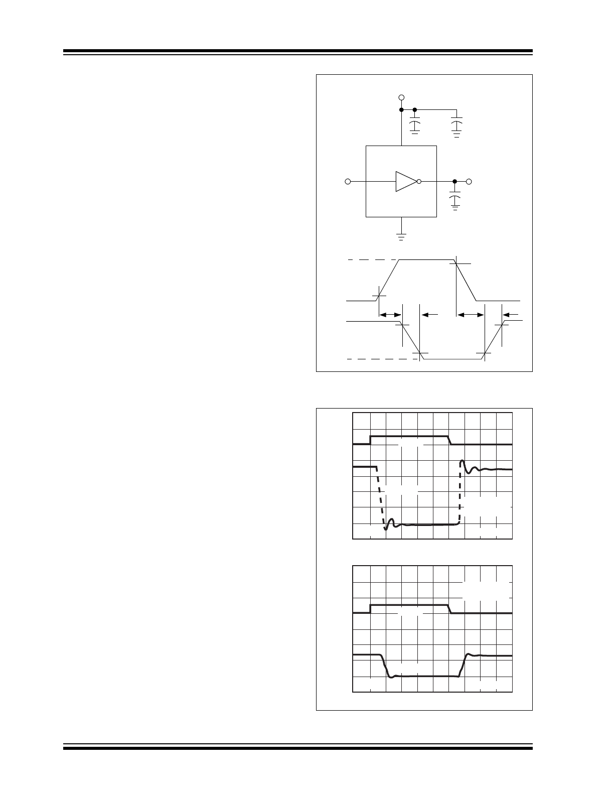
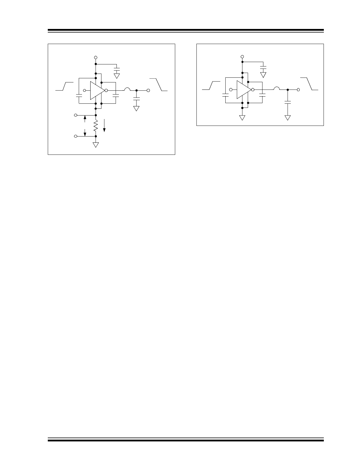
FIGURE 4-1:
Inverting Driver Switching
Time Test Circuit.
FIGURE 4-2:
Switching Speed.
C
L
= 2500 pF
0.1 µF
1 µF
Input
V
DD
= 18V
Output
Input: 100 kHz,
square wave,
t
RISE
= t
FALL
10 nsec
4, 5
2
6, 7
1, 8
TC429
t
R
Output
Input
t
D1
t
F
t
D2
+5V
10%
90%
10%
90%
10%
90%
18V
0V
0V
TIME (100ns/DIV)
V
O
L
T
A
GE (5V/DIV)
CL = 2500pF
V
S
= 18V
5V
INPUT
OUTPUT
100ns
TIME (100ns/DIV)
V
O
L
T
A
GE (5V/DIV)
CL = 2500pF
V
S
= 7V
5V
INPUT
OUTPUT
100ns
2002-2012 Microchip Technology Inc.
DS21416D-page 9
TC429
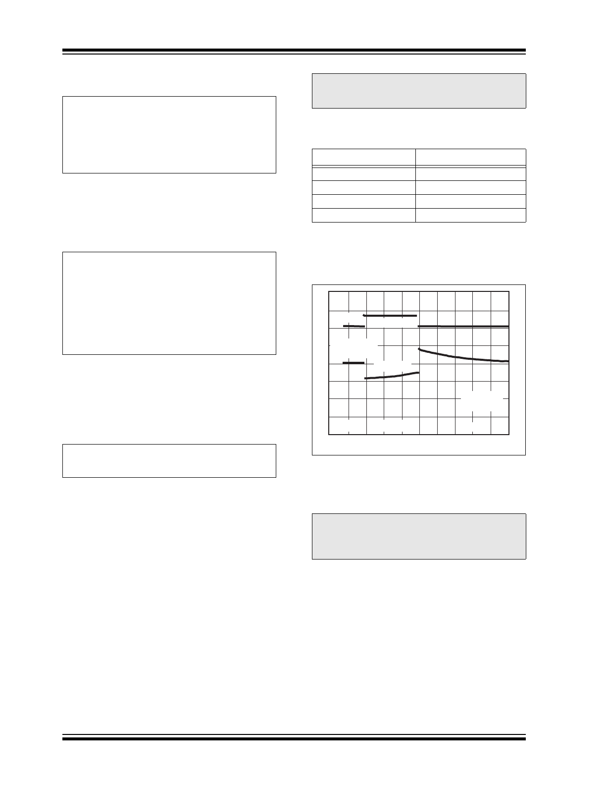
FIGURE 4-3:
Switching Time Degradation
Due To Negative Feedback.
4.3
Input Stage
The input voltage level changes the no-load or
quiescent supply current. The N-channel MOSFET
input stage transistor drives a 3 mA current source
load. With a logic ‘1’ input, the maximum quiescent
supply current is 5 mA. Logic ‘0’ input level signals
reduce quiescent current to 500 µA maximum.
The TC429 input is designed to provide 300 mV of
hysteresis, providing clean transitions and minimizing
output stage current spiking when changing states.
Input voltage levels are approximately 1.5V, making the
device TTL-compatible over the 7V to 18V operating
supply range. Input pin current draw is less than 10 µA
over this range.
The TC429 can be directly driven by TL494, SG1526/
1527, SG1524, SE5560 or similar switch-mode
power supply integrated circuits. By off-loading the
power-driving duties to the TC429, the power supply
controller can operate at lower dissipation, improving
performance and reliability.
FIGURE 4-4:
Peak Output Current Test
Circuit.
4.4
Power Dissipation
CMOS circuits usually permit the user to ignore power
dissipation. Logic families such as the 4000 and 74C
have outputs that can only supply a few milliamperes of
current, and even shorting outputs to ground will not
force enough current to destroy the device. The TC429,
however, can source or sink several amperes and drive
large capacitive loads at high frequency. Since the
package power dissipation limit can easily be
exceeded, some attention should be given to power
dissipation when driving low-impedance loads and/or
operating at high frequency.
The supply current versus frequency and supply
current versus capacitive load characteristic curves will
aid in determining power dissipation calculations.
Table 4-1 lists the maximum operating frequency for
several power supply voltages when driving a 2500 pF
load. More accurate power dissipation figures can be
obtained by summing the three components that make
up the total device power dissipation.
Input signal duty cycle, power supply voltage and
capacitive load influence package power dissipation.
Given power dissipation and package thermal resis-
tance, the maximum ambient operation temperature
is easily calculated. The 8-pin CERDIP junction-to-
ambient thermal resistance is 150
C/W. At +25C, the
package is rated at 800 mW maximum dissipation.
Maximum allowable junction temperature is +150
C.
Three components make up total package power
dissipation:
• Capacitive load dissipation (P
C
)
• Quiescent power (P
Q
)
• Transition power (P
T
)
The capacitive load-caused dissipation is a direct
function of frequency, capacitive load and supply
voltage.
TC429
1 µF
0.1 µF
0.1 µF
0V
18V
2.4V
0V
Logic
Ground
Power
Ground
300 mV
6A
PC Trace Resistance = 0.05
2500 pF
1
8 6,7
5
4
2
+18V
TEK Current
Probe 6302
TC429
1 µF
0.1 µF
0.1 µF
0V
18V
2.4V
0V
2500 pF
1
8
6,7
5
4
2
TEK Current
Probe 6302
+18V
TC429
DS21416D-page 10
2002-2012 Microchip Technology Inc.
The device capacitive load dissipation is:
EQUATION
Quiescent power dissipation depends on input signal
duty cycle. A logic low input results in a low-power
dissipation mode with only 0.5 mA total current drain.
Logic-high signals raise the current to 5 mA maximum.
The quiescent power dissipation is:
EQUATION
Transition power dissipation arises because the output
stage N- and P-channel MOS transistors are ON
simultaneously for a very short period when the output
changes.
The device transition power dissipation is approxi-
mately:
EQUATION
An example shows the relative magnitude for each
item.
TABLE 4-1:
MAXIMUM OPERATING
FREQUENCIES
FIGURE 4-5:
Peak Output Current
Capability.
4.5
POWER-ON OSCILLATION
Power-on oscillations are due to trace size, layout and
component placement. A ‘quick fix’ for most applica-
tions that exhibit power-on oscillation problems is to
place approximately 10 k
in series with the input of
the MOSFET driver.
C
= 2500 pF
V
S
= 15V
D
= 50%
f
= 200 kHz
P
D
= Package power dissipation:
= P
C
+ P
T
+ P
Q
= 113 mW + 10 mW + 41 mW
= 164 mW
Maximum ambient operating temperature:
= T
J
–
JA
(P
D
)
= 150ºC - (150ºC/W)(0.164W)
= 125
C
Where:
T
J
= Maximum allowable junction temperature
(+150
C)
JA
= Junction-to-ambient thermal resistance
(150
C/W, CERDIP)
P
C
fCV
S
2
=
Where:
f = Switching frequency
C = Capacitive load
V
S
= Supply voltage
P
Q
V
S
D I
H
1
D
–
I
L
+
=
Where:
I
H
= Quiescent current with input high
I
L
= Quiescent current with input low
D = Duty cycle
(5 mA max)
(0.5 mA max)
P
T
fV
S
3.3
10
9
–
A
Sec
=
Note:
Ambient operating temperature should not
exceed +85ºC for EPA or EOA devices or
+125ºC for MJA devices.
V
S
f
MAX
18V
500 kHz
15V
700 kHz
10V
1.3 MHz
5V
>2 MHz
Conditions:
1.
CERDIP Package (
JA
=150
C/W)
2.
T
A
= +25
C
3.
C
L
= 2500 pF
Note:
It is extremely important that all MOSFET
driver applications be evaluated for the
possibility of having high-power oscillations
occur during the power-on cycle.
TIME (5
μs/DIV)
V
S
= 18V
R
L
= 0.1
Ω
5V
INPUT
OUTPUT
5
μs
500mV
5V/DIV
500mV/DIV
(5 AMP/DIV)