
2002-2012 Microchip Technology Inc.
DS21415D-page 1
TC426/TC427/TC428
Features:
• High-Speed Switching (C
L
= 1000 pF): 30 nsec
• High Peak Output Current: 1.5A
• High Output Voltage Swing:
- V
DD
-25 mV
- GND +25 mV
• Low Input Current (Logic ‘0’ or ‘1’): 1
A
• TTL/CMOS Input Compatible
• Available in Inverting and Noninverting
Configurations
• Wide Operating Supply Voltage:
- 4.5V to 18V
• Current Consumption:
- Inputs Low – 0.4 mA
- Inputs High – 8 mA
• Single Supply Operation
• Low Output Impedance: 6
• Pinout Equivalent of DS0026 and MMH0026
• Latch-Up Resistant: Withstands > 500 mA
Reverse Current
• ESD Protected: 2 kV
Applications:
• Switch Mode Power Supplies
• Pulse Transformer Drive
• Clock Line Driver
• Coax Cable Driver
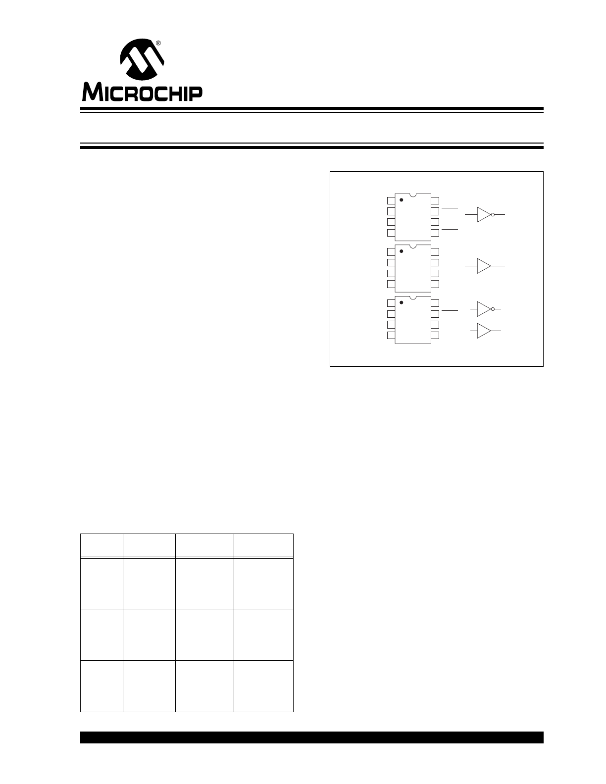
Device Selection Table
Package Type
General Description:
The TC426/TC427/TC428 are dual CMOS high-speed
drivers. A TTL/CMOS input voltage level is translated
into a rail-to-rail output voltage level swing. The CMOS
output is within 25 mV of ground or positive supply.
The low-impedance, high-current driver outputs swing
a 1000 pF load 18V in 30 nsec. The unique current and
voltage drive qualities make the TC426/TC427/TC428
ideal power MOSFET drivers, line drivers, and DC-to-
DC converter building blocks.
Input logic signals may equal the power supply voltage.
Input current is a low 1
A, making direct interface
to CMOS/bipolar switch-mode power supply control
ICs possible, as well as open-collector analog
comparators.
Quiescent power supply current is 8 mA maximum. The
TC426 requires 1/5 the current of the pin-compatible
bipolar DS0026 device. This is important in DC-to-DC
converter applications with power efficiency constraints
and high-frequency switch-mode power supply
applications. Quiescent current is typically 6 mA when
driving a 1000 pF load 18V at 100 kHz.
The inverting TC426 driver is pin-compatible with the
bipolar DS0026 and MMH0026 devices. The TC427 is
noninverting; the TC428 contains an inverting and non-
inverting driver.
Other pin compatible driver families are the TC1426/
TC1427/TC1428, TC4426/TC4427/TC4428 and
TC4426A/TC4427A/TC4428A.
Part
Number
Package
Configuration
Temp.
Range
TC426COA
TC426CPA
TC426EOA
TC426EPA
TC426IJA
TC426MJA
8-Pin SOIC
8-Pin PDIP
8-Pin SOIC
8-Pin PDIP
8-Pin CERDIP
8-Pin CERDIP
Inverting
Inverting
Inverting
Inverting
Inverting
Inverting
0°C to +70°C
0°C to +70°C
-40°C to +85°C
-40°C to +85°C
-25°C to +85°C
-55°C to +125°C
TC427COA
TC427CPA
TC427EOA
TC427EPA
TC427IJA
TC427MJA
8-Pin SOIC
8-Pin PDIP
8-Pin SOIC
8-Pin PDIP
8-Pin CERDIP
8-Pin CERDIP
Noninverting
Noninverting
Noninverting
Noninverting
Noninverting
Noninverting
0°C to +70°C
0°C to +70°C
-40°C to +85°C
-40°C to +85°C
-25°C to +85°C
-55°C to +125°C
TC428COA
TC428CPA
TC428EOA
TC428EPA
TC428IJA
TC428MJA
8-Pin SOIC
8-Pin PDIP
8-Pin SOIC
8-Pin PDIP
8-Pin CERDIP
8-Pin CERDIP
Complementary
Complementary
Complementary
Complementary
Complementary
Complementary
0°C to +70°C
0°C to +70°C
-40°C to +85°C
-40°C to +85°C
-25°C to +85°C
-55°C to +125°C
TC426
1
2
3
4
NC
5
6
7
8
OUT A
OUT B
NC
IN A
GND
IN B
NC = No internal connection
2, 4
7, 5
Inverting
TC427
1
2
3
4
NC
5
6
7
8
OUT A
OUT B
NC
IN A
GND
IN B
2, 4
7, 5
Noninverting
TC428
1
2
3
4
NC
5
6
7
8
OUT A
OUT B
NC
IN A
GND
IN B
2
7
4
5
V
DD
Complementary
V
DD
V
DD
8-Pin PDIP/SOIC/CERDIP
1.5A Dual High-Speed Power MOSFET Drivers
TC426/TC427/TC428
DS21415D-page 2
2002-2012 Microchip Technology Inc.
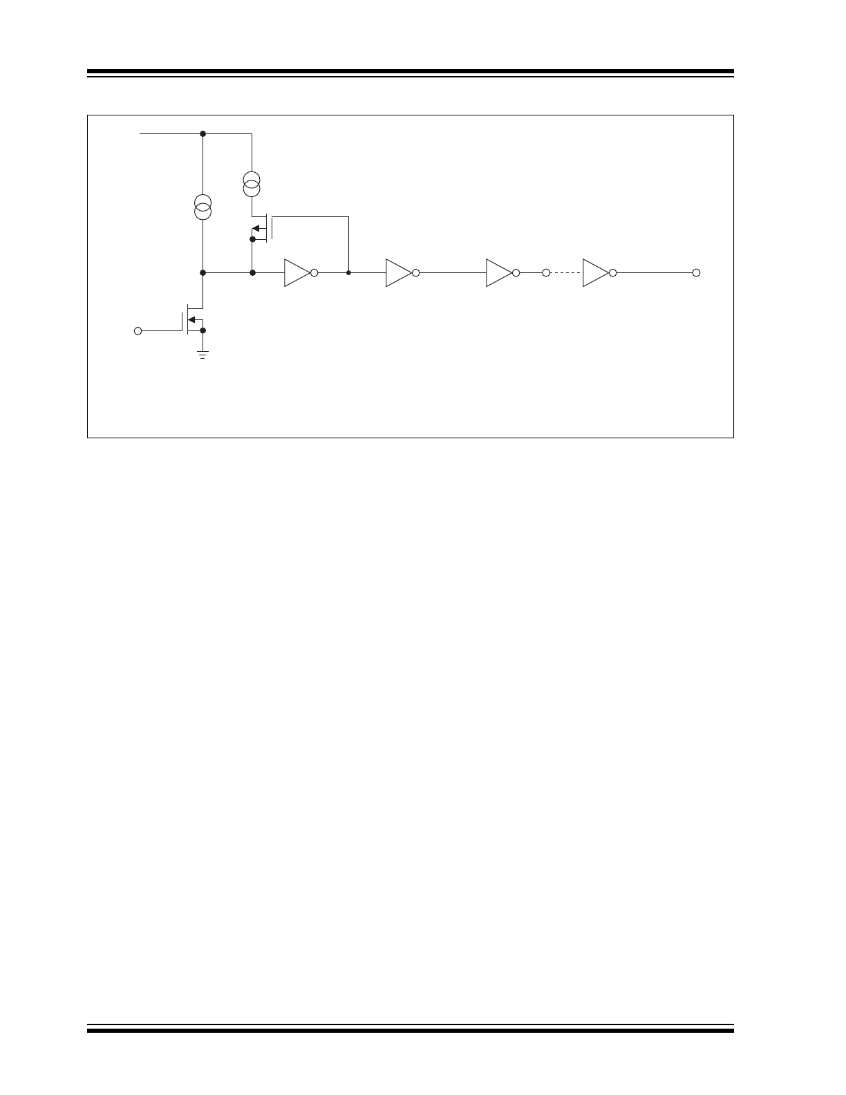
Functional Block Diagram
Input
V+
≈2.5
μ
A
≈500
μ
A
NOTE: TC428 has one inverting and one noninverting driver.
Ground any unused driver input.
Inverting
Output
Noninverting
Output
(TC426)
(TC427)
GND
TC426
TC427
TC428
2002-2012 Microchip Technology Inc.
DS21415D-page 3
TC426/TC427/TC428
1.0
ELECTRICAL
CHARACTERISTICS
Absolute Maximum Ratings*
Supply Voltage ..................................................... +20V
Input Voltage, Any Terminal
................................... V
DD
+ 0.3V to GND – 0.3V
Power Dissipation (T
A
70°C)
PDIP........................................................ 730 mW
CERDIP .................................................. 800 mW
SOIC ....................................................... 470 mW
Derating Factor
PDIP....................................................... 8 mW/°C
CERDIP .............................................. 6.4 mW/°C
SOIC ...................................................... 4 mW/°C
Operating Temperature Range
C Version ........................................ 0°C to +70°C
I Version ....................................... -25°C to +85°C
E Version...................................... -40°C to +85°C
M Version ................................... -55°C to +125°C
Storage Temperature Range .............. -65°C to +150°C
*Stresses above those listed under “Absolute
Maximum Ratings” may cause permanent damage to
the device. These are stress ratings only and functional
operation of the device at these or any other conditions
above those indicated in the operation sections of the
specifications is not implied. Exposure to Absolute
Maximum Rating conditions for extended periods may
affect device reliability.
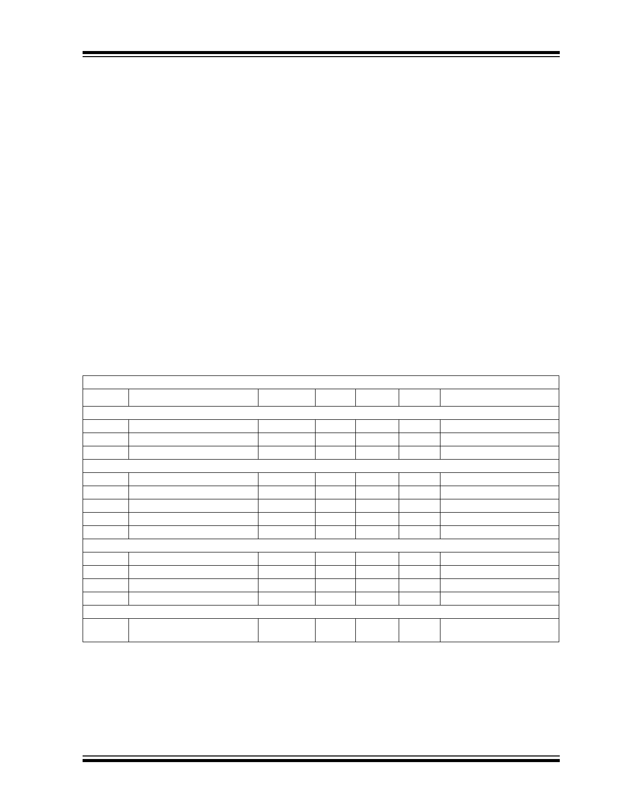
TC426/TC427/TC428 ELECTRICAL SPECIFICATIONS
Electrical Characteristics: T
A
= +25°C with 4.5V
V
DD
18V, unless otherwise noted.
Symbol
Parameter
Min
Typ
Max
Units
Test Conditions
Input
V
IH
Logic 1, High Input Voltage
2.4
—
—
V
V
IL
Logic 0, Low Input Voltage
—
—
0.8
V
I
IN
Input Current
-1
—
1
A
0V
V
IN
V
DD
Output
V
OH
High Output Voltage
V
DD
– 0.025
—
—
V
V
OL
Low Output Voltage
—
—
0.025
V
R
OH
High Output Resistance
—
10
15
I
OUT
= 10 mA, V
DD
= 18V
R
OL
Low Output Resistance
—
6
10
I
OUT
= 10 mA, V
DD
= 18V
I
PK
Peak Output Current
—
1.5
—
A
Switching Time (Note 1)
t
R
Rise Time
—
—
30
nsec
Figure 3-1, Figure 3-2
t
F
Fall Time
—
—
30
nsec
Figure 3-1, Figure 3-2
t
D1
Delay Time
—
—
50
nsec
Figure 3-1, Figure 3-2
t
D2
Delay Time
—
—
75
nsec
Figure 3-1, Figure 3-2
Power Supply
I
S
Power Supply Current
—
—
—
—
8
0.4
mA
V
IN
= 3V (Both Inputs)
V
IN
= 0V (Both Inputs)
Note
1:
Switching times ensured by design.
TC426/TC427/TC428
DS21415D-page 4
2002-2012 Microchip Technology Inc.
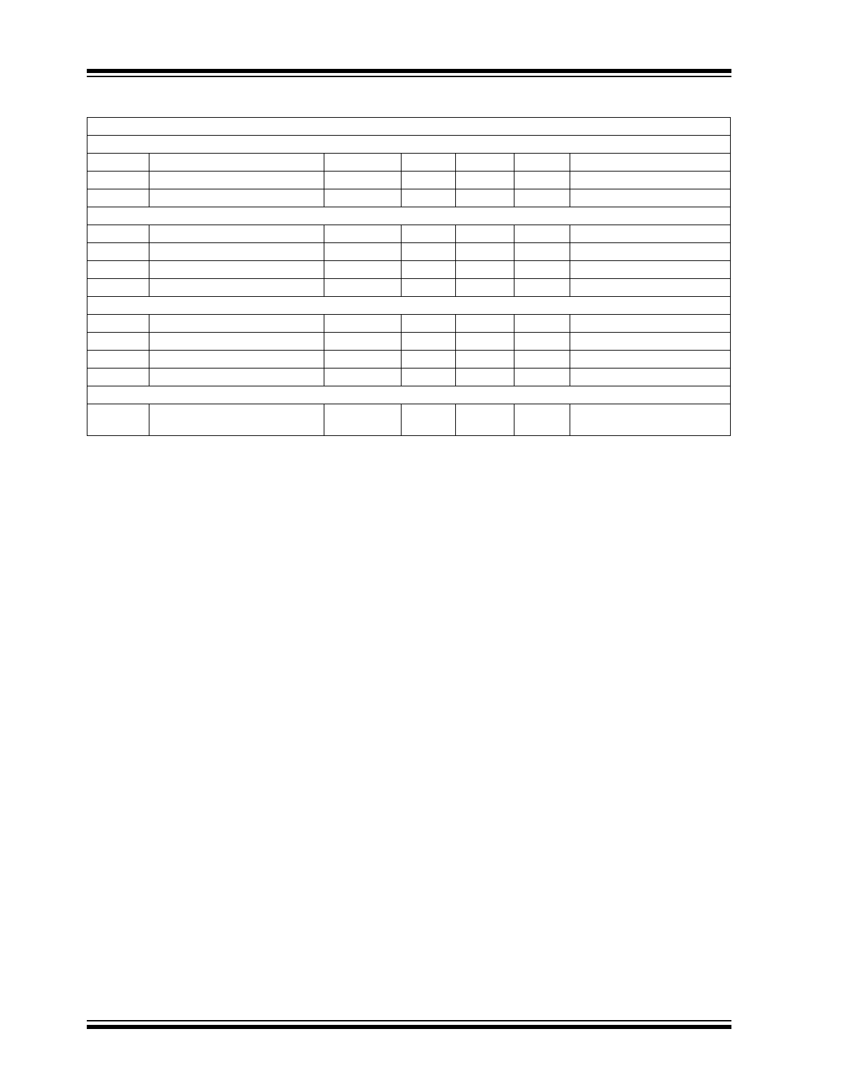
TC426/TC427/TC428 ELECTRICAL SPECIFICATIONS (CONTINUED)
Electrical Characteristics: Over operating temperature range with 4.5V
V
DD
18V, unless otherwise noted.
Input
V
IH
Logic 1, High Input Voltage
2.4
—
—
V
V
IL
Logic 0, Low Input Voltage
—
—
0.8
V
I
IN
Input Current
-10
—
10
A
0V
V
IN
V
DD
Output
V
OH
High Output Voltage
V
DD
– 0.025
—
—
V
V
OL
Low Output Voltage
—
—
0.025
V
R
OH
High Output Resistance
—
13
20
I
OUT
= 10 mA, V
DD
= 18V
R
OL
Low Output Resistance
—
8
15
I
OUT
= 10 mA, V
DD
= 18V
Switching Time (Note 1)
t
R
Rise Time
—
—
60
nsec
Figure 3-1, Figure 3-2
t
F
Fall Time
—
—
60
nsec
Figure 3-1, Figure 3-2
t
D1
Delay Time
—
—
75
nsec
Figure 3-1, Figure 3-2
t
D2
Delay Time
—
—
120
nsec
Figure 3-1, Figure 3-2
Power Supply
I
S
Power Supply Current
—
—
—
—
12
0.6
mA
V
IN
= 3V (Both Inputs)
V
IN
= 0V (Both Inputs)
Note
1:
Switching times ensured by design.
2002-2012 Microchip Technology Inc.
DS21415D-page 5
TC426/TC427/TC428
2.0
PIN DESCRIPTIONS
The descriptions of the pins are listed in Table 2-1.
TABLE 2-1:
PIN FUNCTION TABLE
Pin No.
(8-Pin PDIP,
SOIC, CERDIP)
Symbol
Description
1
NC
No Internal Connection.
2
IN A
Control Input A, TTL/CMOS compatible logic input.
3
GND
Ground.
4
IN B
Control Input B, TTL/CMOS compatible logic input.
5
OUT B
CMOS totem-pole output.
6
V
DD
Supply input, 4.5V to 18V.
7
OUT A
CMOS totem-pole output.
8
NC
No internal Connection.

TC426/TC427/TC428
DS21415D-page 6
2002-2012 Microchip Technology Inc.
3.0
APPLICATIONS INFORMATION
3.1
Supply Bypassing
Charging and discharging large capacitive loads
quickly requires large currents. For example, charging
a 1000 pF load to 18V in 25 nsec requires an 0.72A
current from the device power supply.
To ensure low supply impedance over a wide frequency
range, a parallel capacitor combination is recom-
mended for supply bypassing. Low-inductance ceramic
disk capacitors with short lead lengths (< 0.5 in.) should
be used. A 1
F film capacitor in parallel with one or two
0.1
F ceramic disk capacitors normally provides
adequate bypassing.
3.2
Grounding
The TC426 and TC428 contain inverting drivers.
Ground potential drops developed in common ground
impedances from input to output will appear as
negative feedback and degrade switching speed
characteristics.
Individual ground returns for the input and output
circuits or a ground plane should be used.
3.3
Input Stage
The input voltage level changes the no-load or
quiescent supply current. The N-channel MOSFET
input stage transistor drives a 2.5 mA current source
load. With a logic ‘1’ input, the maximum quiescent
supply current is 8 mA. Logic ‘0’ input level signals
reduce quiescent current to 0.4 mA maximum.
Minimum power dissipation occurs for logic ‘0’ inputs
for the TC426/TC427/TC428. Unused driver inputs
must be connected to V
DD
or GND.
The drivers are designed with 100 mV of hysteresis.
This provides clean transitions and minimizes output
stage current spiking when changing states. Input
voltage thresholds are approximately 1.5V, making the
device TTL compatible over the 4.5V to 18V supply
operating range. Input current is less than 1
A over
this range.
The TC426/TC427/TC428 may be directly driven by
the TL494, SG1526/1527, SG1524, SE5560, and
similar switch-mode power supply integrated circuits.
3.4
Power Dissipation
The supply current vs frequency and supply current
vs capacitive load characteristic curves will aid in
determining power dissipation calculations.
The TC426/TC427/TC428 CMOS drivers have greatly
reduced quiescent DC power consumption. Maximum
quiescent current is 8 mA compared to the DS0026 40
mA specification. For a 15V supply, power dissipation
is typically 40 mW.
Two other power dissipation components are:
• Output stage AC and DC load power.
• Transition state power.
Output stage power is:
Po = P
DC
+ PAC
= Vo (I
DC
) + f C
L
V
S
2
Where:
Vo = DC output voltage
I
DC
= DC output load current
f
= Switching frequency
Vs = Supply voltage
In power MOSFET drive applications the P
DC
term is
negligible. MOSFET power transistors are high-imped-
ance, capacitive input devices. In applications where
resistive loads or relays are driven, the P
DC
component
will normally dominate.
The magnitude of P
AC
is readily estimated for several
cases:
A.
B.
1. f
= 200 kHZ
1. f
= 200 kHz
2. C
L
=1000 pf
2. C
L
=1000 pf
3. Vs
= 18V
3. Vs
= 15V
4. P
AC
= 65 mW
4. P
AC
= 45 mW
During output level state changes, a current surge will
flow through the series connected N and P channel
output MOSFETS as one device is turning “ON” while
the other is turning “OFF”. The current spike flows only
during output transitions. The input levels should not be
maintained between the logic ‘0’ and logic ‘1’ levels.
Unused driver inputs must be tied to ground and
not be allowed to float. Average power dissipation will
be reduced by minimizing input rise times. As shown in
the characteristic curves, average supply current is
frequency dependent.
2002-2012 Microchip Technology Inc.
DS21415D-page 7
TC426/TC427/TC428
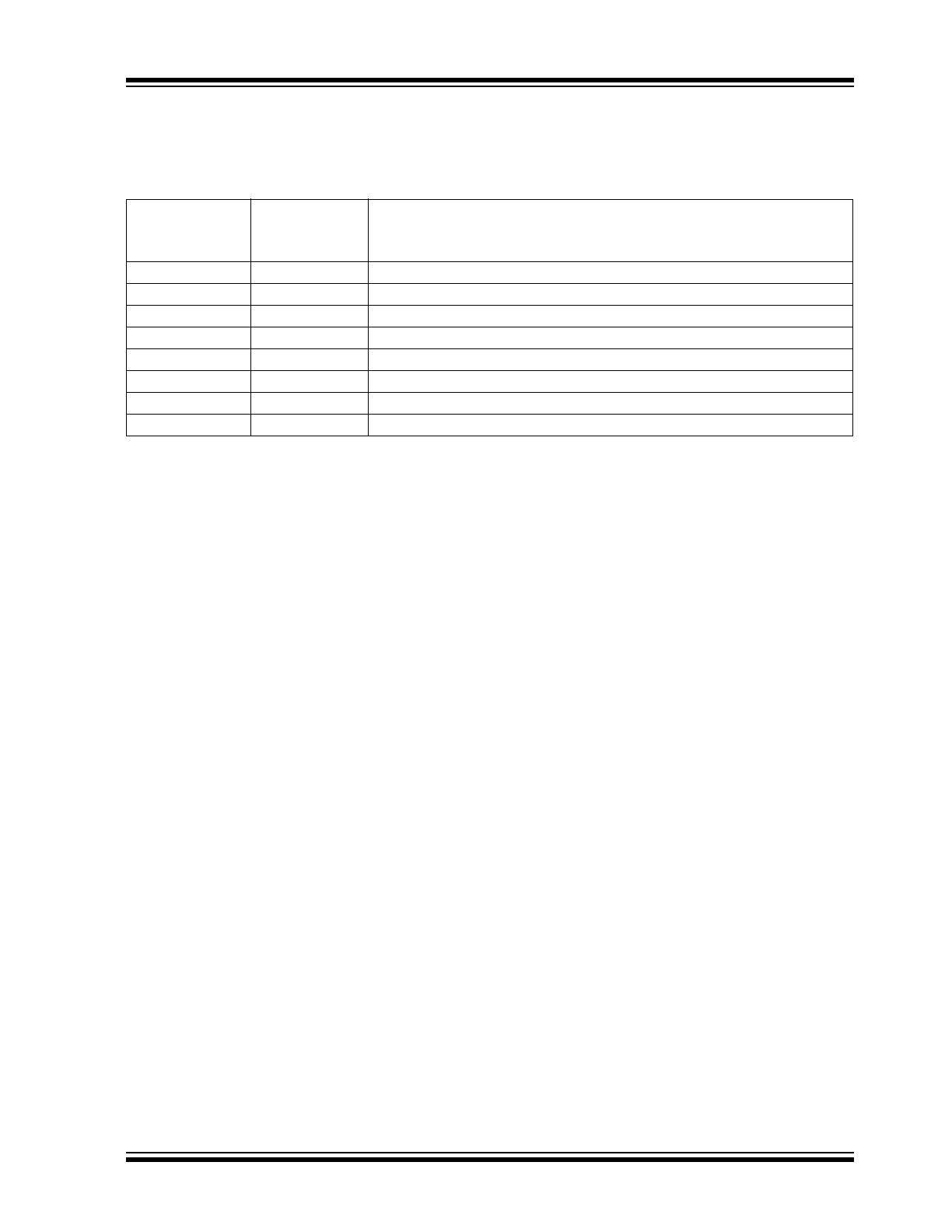
FIGURE 3-1:
Inverting Driver Switching
Time Test Circuit
FIGURE 3-2:
Noninverting Driver
Switching Time Test Circuit
FIGURE 3-3:
Voltage Doubler
FIGURE 3-4:
Voltage Inverter
Output
Input
0.1
μ
F
V
DD
= 18V
+5V
Input
10%
90%
10%
90%
10%
90%
18V
Output
t
D1
t
F
t
R
t
D2
C
L
= 1000 pF
1
μ
F
0V
0V
TC426
(1/2 TC428)
1
2
Input: 100 kHz,
square wave,
t
RISE
= t
FALL
≤ 10 nsec
Output
Input
90%
10%
10%
10%
90%
TC427
(1/2 TC428)
+5V
Input
18V
Output
0V
0V
90%
1
2
0.1
μ
F
1
μ
F
t
D1
t
F
t
R
t
D2
V
DD
= 18V
C
L
= 1000 pF
Input: 100 kHz,
square wave,
t
RISE
= t
FALL
≤ 10 nsec
+15V
0.1
μ
F
4.7
μ
F
10
μ
F
47
μ
F
+
–
+
–
+
–
1N4001
1N4001
V
OUT
f
IN
= 10 kHz
2
6
3
7
29.
27.
25.
23.
0
10
20 30 40 50 60 70 80 90
I
OUT
(mA)
28.
26.
24.
22.
30.
100
V
OUT
(V)
1/2
TC426
+15V
0.1
μ
F 4.7
μ
F
10
μ
F
47
μ
F
+
–
+
–
1N4001
1N4001
2
6
3
7
1/2
TC426
+
–
-6
-8
-10
-12
0
10 20 30 40 50 60 70 80 90
-7
-9
-11
-13
-5
-14
100
I
OUT
(mA)
V
OUT
(V)
V
OUT
f
IN
= 10 kHz
TC426/TC427/TC428
DS21415D-page 8
2002-2012 Microchip Technology Inc.
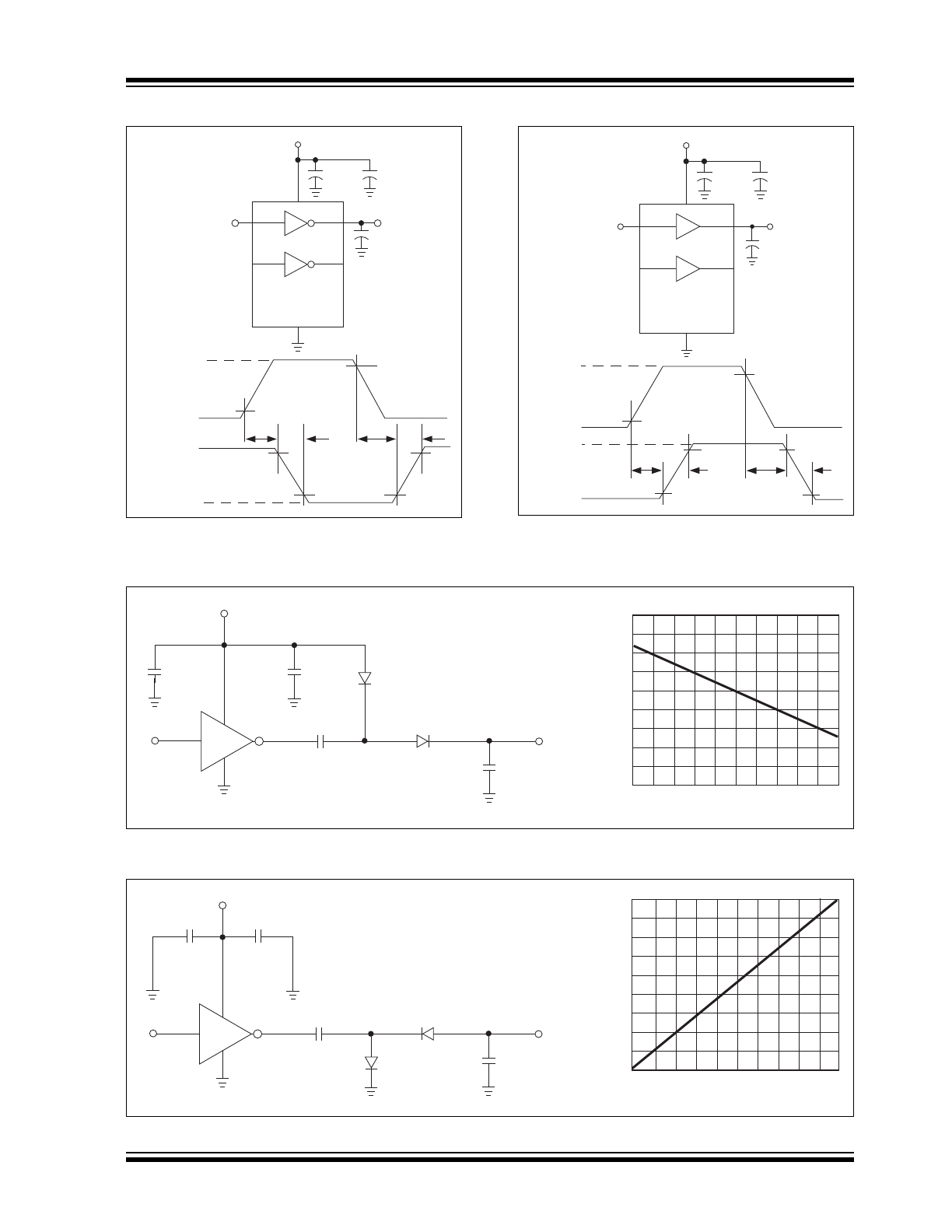
4.0
TYPICAL CHARACTERISTICS
Note:
The graphs and tables provided following this note are a statistical summary based on a limited number of
samples and are provided for informational purposes only. The performance characteristics listed herein
are not tested or guaranteed. In some graphs or tables, the data presented may be outside the specified
operating range (e.g., outside specified power supply range) and therefore outside the warranted range.
30
20
10
0
-25
0
25
150
TIME (ns)
Rise and Fall Times vs.
Temperature
40
50
75
100
125
TEMPERATURE (°C)
35
25
15
80
70
60
50
30
0
DELA
Y
TIME (ns)
Delay Times vs. Supply Voltage
40
90
SUPPLY VOLTAGE (V)
5
10
15
20
t
D2
60
50
40
30
10
0
5
10
15
20
TIME (ns)
SUPPLY VOLTAGE (V)
70
t
R
t
F
C
L
= 1000 pF
T
A
= +25°C
Rise and Fall Times vs.
Supply Voltage
20
C
L
= 1000 pF
T
A
= +25°C
C
L
= 1000 pF
V
DD
= 18V
t
R
t
F
t
D1
100
1
10
1000
10K
TIME (ns)
CAPACITIVE LOAD (pF)
Rise and Fall Times vs.
Capacitive Load
10
1K
100
90
80
70
60
40
30
0
-25
50
100
150
DELA
Y
TIME (ns)
TEMPERATURE (°C)
Delay Times vs. Temperature
50
100
25
75
125
70
60
50
40
20
0
10
SUPPL
Y
CURRENT (mA)
Supply Current vs.
Capacitive Load
30
80
400 kHz
200 kHz
20 kHz
100
1000
10K
CAPACITIVE LOAD (pF)
10
C
L
= 1000 pF
V
DD
= 18V
t
D2
t
D1
T
A
= +25°C
V
DD
= 18V
T
A
= +25°C
V
DD
= 18V
t
R
t
F
0.96
0.72
0.48
0.24
0
10
OUTPUT VOL
T
AGE (V)
Low Output vs. Voltage
1.20
20 30 40 50 60 70 80 90 100
CURRENT SUNK (mA)
10V
15V
1.76
1.32
0.88
0.44
0
10
High Output vs. Voltage
2.20
20 30 40 50 60 70 80 90 100
CURRENT SOURCED (mA)
18V
V
DD
– V
OUT
(V)
⎥⎥
13V
20
10
0
1
SUPPL
Y
CURRENT (mA)
Supply Current vs. Frequency
30
10
100
1000
FREQUENCY (kHz)
10V
5V
T
A
= +25°C
V
DD
= 5V
V
DD
= 8V
V
DD
= 18V
C
L
= 1000 pF
T
A
= +25°C
T
A
= +25°C
2002-2012 Microchip Technology Inc.
DS21415D-page 9
TC426/TC427/TC428
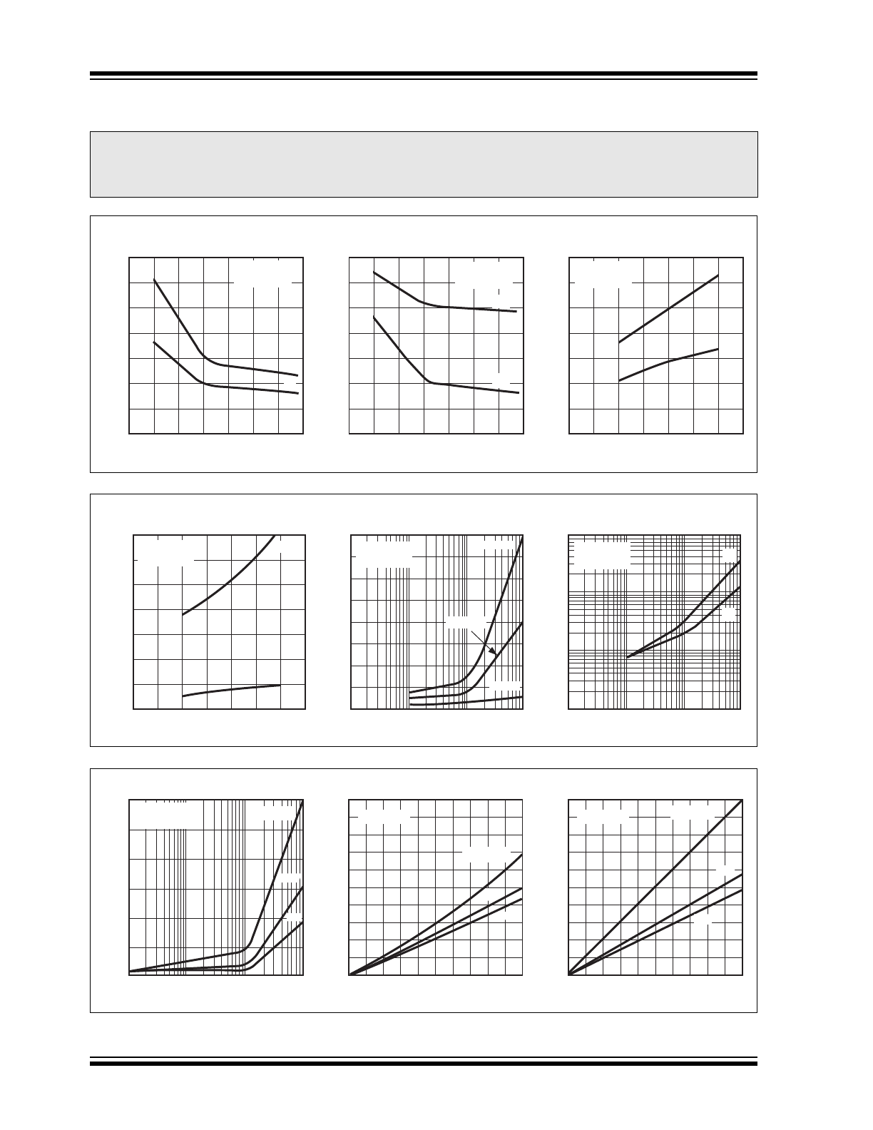
TYPICAL CHARACTERISTICS (CONTINUED)
0
20
15
10
5
0
SUPPL
Y
VOL
T
AGE (V)
50
100
150
200
250
300
SUPPLY CURRENT (mA)
Supply Voltage vs.
Quiescent Supply Current
No Load
Both Inputs Logic ‘0’
T
A
= +25°C
1
2
3
4
5
6
20
15
10
5
0
SUPPL
Y
VOL
T
AGE (V)
SUPPLY CURRENT (mA)
Supply Voltage vs.
Quiescent Supply Current
No Load
Both Inputs Logic ‘1’
T
A
= +25°C
200
0
400
600
800
1000
1200
1400
1600
0
10
20
30
40
50
60
70
80
90
100
110
120
AMBIENT TEMPERATURE (°C)
MAX. POWER (mW)
8-Pin DIP
8-Pin CERDIP
8-Pin SOIC
Thermal Derating Curves
TC426/TC427/TC428
DS21415D-page 10
2002-2012 Microchip Technology Inc.
5.0
PACKAGING INFORMATION
5.1
Package Marking Information
Package marking data not available at this time.
5.2
Taping Form
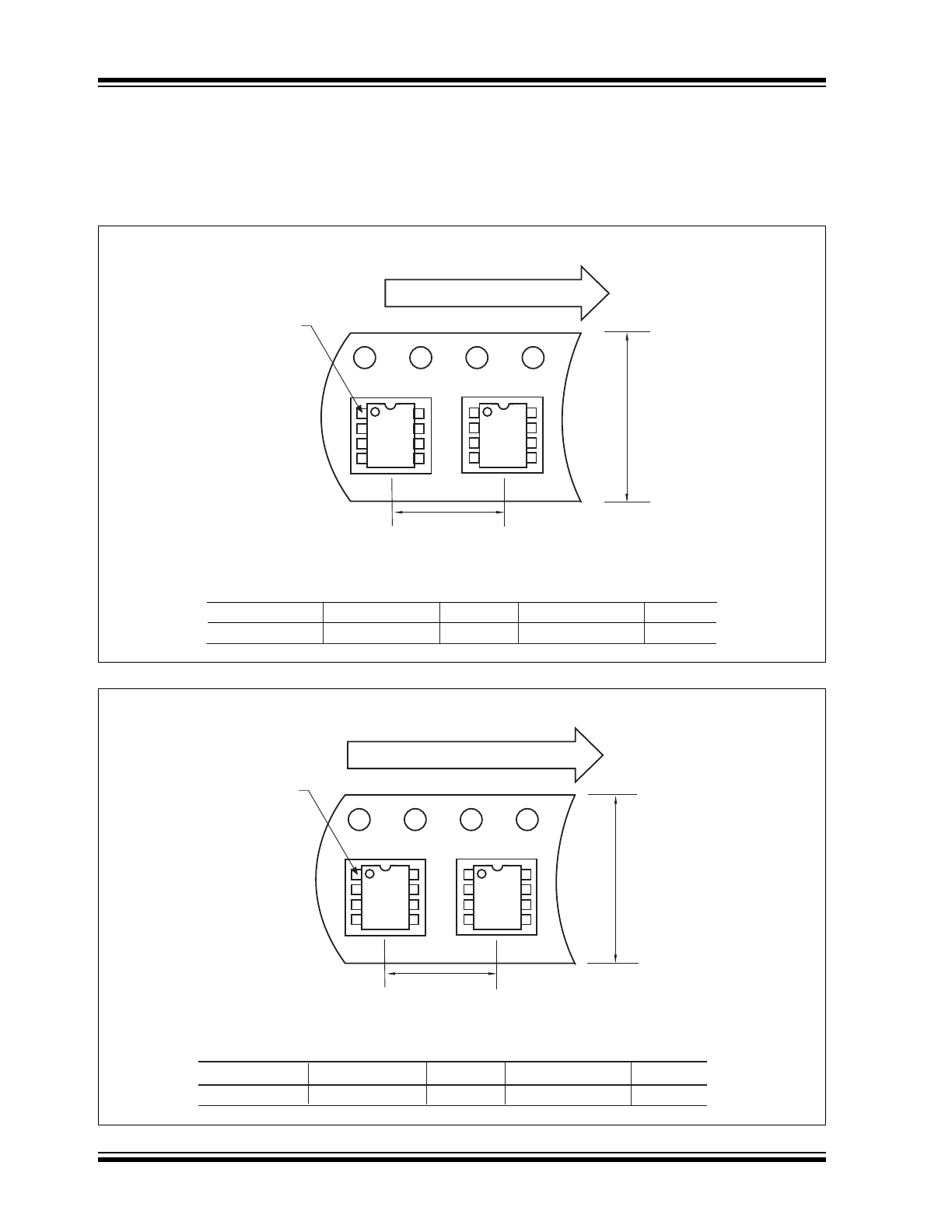
Component Taping Orientation for 8-Pin MSOP Devices
Package
Carrier Width (W)
Pitch (P)
Part Per Full Reel
Reel Size
8-Pin MSOP
12 mm
8 mm
2500
13 in
Carrier Tape, Number of Components Per Reel and Reel Size
Pin 1
User Direction of Feed
Standard Reel Component Orientation
for 713 Suffix Device
W
P
Component Taping Orientation for 8-Pin SOIC (Narrow) Devices
Package
Carrier Width (W)
Pitch (P)
Part Per Full Reel
Reel Size
8-Pin SOIC (N)
12 mm
8 mm
2500
13 in
Carrier Tape, Number of Components Per Reel and Reel Size
Standard Reel Component Orientation
for 713 Suffix Device
Pin 1
User Direction of Feed
P
W