
2001-2012 Microchip Technology Inc.
DS21402D-page 1
TC32M
Features:
• Incorporates the Functionality of the Industry
Standard TC1232 (Processor Monitor, Watchdog
and Manual Override Reset Controller) into a
Small, Lower Cost Package
• Guards Against Unstable Processor Operation
Resulting from Power “Brown-Out”
• Automatically Halts and Restarts an Out-of-
Control Microprocessor
• Output can be Wire-ORed, or Hooked to Manual
Reset Push-button Switch
• Space-Saving 3-Pin TO-92 or SOT-223 Package
Applications:
• All Microprocessor-Based Systems
• Battery Powered Computers and Controllers
• Automotive Systems
• Intelligent Instruments
• Critical Processor Monitoring
• Embedded Controllers
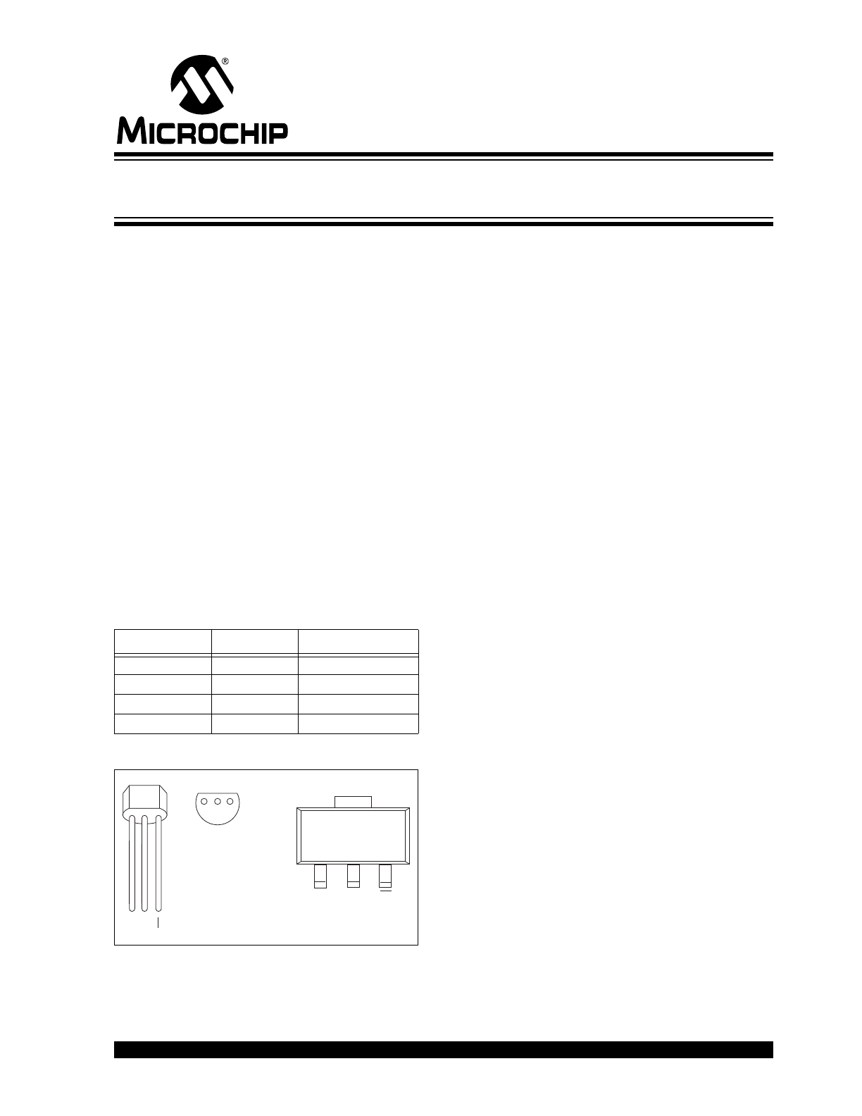
Device Selection Table
Package Type
General Description:
The TC32M is a fully-integrated processor supervisor
in a 3-pin package. It provides three important func-
tions to safeguard processor sanity: precision power
on/off Reset control, Watchdog Timer and external
Reset override.
On power-up, the TC32M holds the processor in the
Reset state for a minimum of 500 msec after V
DD
is
within tolerance to ensure a stable system start-up.
Microprocessor sanity is monitored by the on-board
Watchdog circuit. The microprocessor must provide a
high-to-low level shift (through an external resistor
divider) on the RS pin of the TC32M. Should the
processor fail to supply this signal within the specified
time-out period (typically 700 msec), an out-of-control
processor is indicated and the TC32M issues a
processor Reset as a result.
The output of the TC32M can be wire-ORed with a
push-button switch (or electronic signal) to override the
TC32M and unconditionally reset the processor. When
connected to a push-button switch, the TC32M
provides contact debounce.
The TC32M is packaged in a space-saving TO-92 or
SOT-223 package. It provides all of the functionality of
the industry standard TC1232 in a smaller, lower cost
configuration.
Part Number
Package
Temp. Range
TC32MCDB
SOT-223
0°C to +70°C
TC32MCZB
TO-92
0°C to +70°C
TC32MEDB
SOT-223
-40°C to +85°C
TC32MEZB
TO-92
-40°C to +85°C
1
1
2
4
3
2 3
GND
GND
TC32MCDB
TC32MEDB
TC32MCZB
TC32MEZB
V
DD
V
DD
V
DD
RS
RS
ECONOMONITOR™ – 3-Pin System Supervisor with
Power Supply Monitor and Watchdog
TC32M
DS21402D-page 2
2001-2012 Microchip Technology Inc.
Functional Block Diagram
Typical Operating Circuit
V
DD
V
REF2
V
REF1
TC32M
Watchdog
Timer
RS
GND
DV
Detector
Delay
Timer
5V
R1, 10 k
Ω
R2, 10 k
Ω
RS
TC32M
Microcontroller
Reset
PO.1
Reset
2001-2012 Microchip Technology Inc.
DS21402D-page 3
TC32M
1.0
ELECTRICAL
CHARACTERISTICS
Absolute Maximum Ratings*
Supply Voltage (V
DD
to GND) ............................. +6.0V
Input Voltage Any Pin..... (GND – 0.3V) to (V
DD
+0.3V)
Operating Temperature Range
TC32MC Package........................... 0°C to +70°C
TC32ME Package ........................ -40°C to +85°C
Storage Temperature Range ............. -65°C to +150°C
*Stresses above those listed under “Absolute Maxi-
mum Ratings” may cause permanent damage to the
device. These are stress ratings only and functional
operation of the device at these or any other conditions
above those indicated in the operation sections of the
specifications is not implied. Exposure to Absolute
Maximum Rating conditions for extended periods may
affect device reliability.
TC32M ELECTRICAL SPECIFICATIONS
Recommended DC Operating Conditions: T
A
= -40°C
to
+85
°C unless otherwise noted.
Symbol
Parameter
Min
Typ
Max
Units
Test Conditions
V
DD
Supply Voltage
4.5
—
5.5
V
V
IH
RS Input HIGH Level for PB
2.0
—
—
V
V
IL
RS Input LOW Level for PB
—
—
0.3
V
DC Electrical Characteristics: V
DD
= 4.5V to 5.5V,
T
A
= -40°C
to
+85
°C unless otherwise noted.
Symbol
Parameter
Min
Typ
Max
Units
Test Conditions
I
IL
RS Input Leakage
-1
—
+1
mA
I
OL
RS Output Current
2.0
10
—
mA
V
OL
= 0.4V
I
CC
Operating Current
—
50
200
A
Note 1
V
STH
RS Strobe HIGH Level
(V
DD
– 0.5V)
—
—
V
Figure 3-1
V
STL
RS Strobe LOW Level
2.00
—
(V
DD
– 1.5V)
V
Figure 3-1
V
RST
Reset Threshold
4.25
—
4.50
V
V
DD
Falling (Note 2, Figure 3-3)
Capacitance Electrical Characteristics: T
A
= 25°C
unless otherwise noted.
Symbol
Parameter
Min
Typ
Max
Units
Test Conditions
C
IN
Input Capacitance
—
—
5
pF
C
OUT
Output Capacitance
—
—
7
pF
AC Electrical Characteristics: T
A
= -40°C
to
+85
°C, V
DD
= 5V ±10%,
unless otherwise noted.
Symbol
Parameter
Min
Typ
Max
Units
Test Conditions
t
RST
Reset Active Time
500
700
900
msec Figure
t
ST
RS Strobe Pulse Width
500
—
—
nsec
Figure 3-1
t
TD
Watchdog Time-out Period
500
700
900
msec Figure 3-1
t
RPD
V
DD
Detect to RS LOW
—
—
nsec
Figure 3-1
Note 1:
No output load.
2:
All voltages referenced to ground.
TC32M
DS21402D-page 4
2001-2012 Microchip Technology Inc.
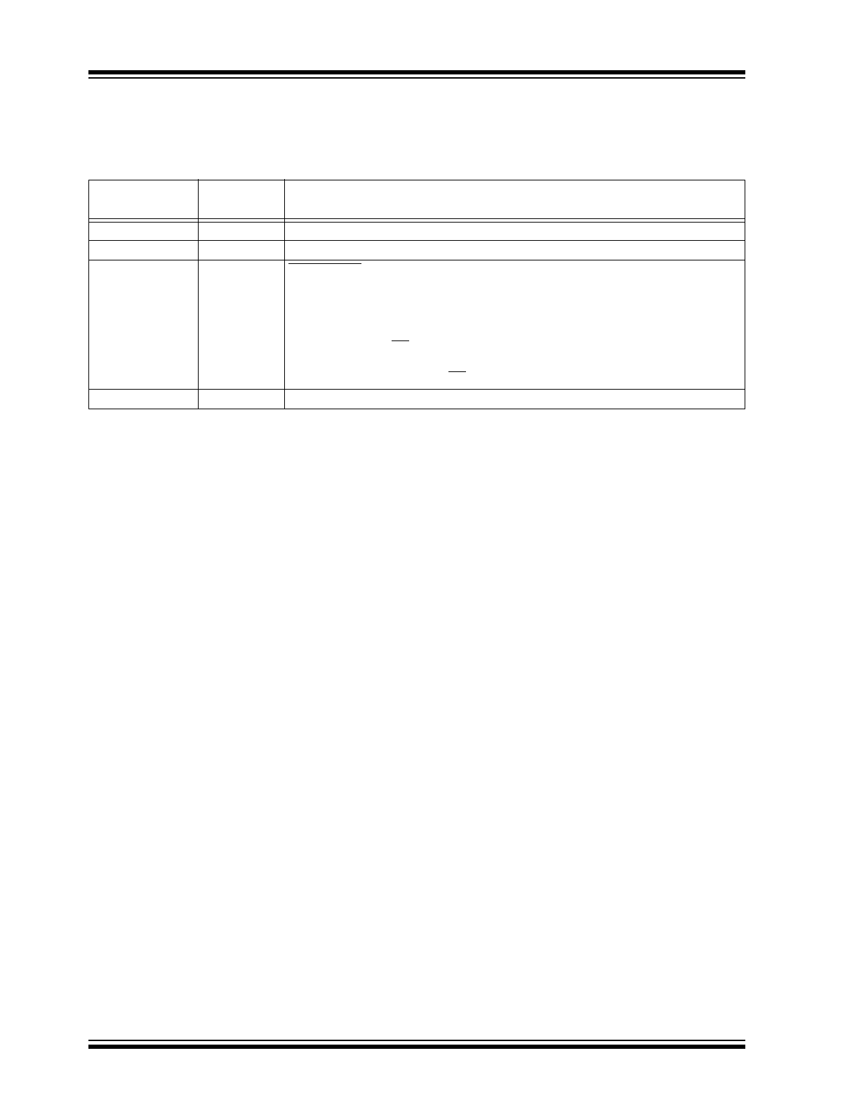
2.0
PIN DESCRIPTIONS
The descriptions of the pins are listed in Table 2-1.
TABLE 2-1:
PIN FUNCTION TABLE
Pin No.
(SOT-223, TO-92)
Symbol
Description
1
GND
Ground.
2
V
DD
The +5V power supply input.
3
RS
Reset/Strobe (Bidirectional). The open drain goes active if:
V
DD
falls below 4.5V nominal.
If pulled low by an external electronic signal or switch closure.
If the Watchdog is not strobed within the minimum Watchdog Time-out period.
During power-up and power-down.
In the Input mode, RS connects to a voltage level shift network (typically a resistor
divider to V
DD
.) The Watchdog Timer is reset when processor causes a voltage
level
V
STL
to be applied to RS.
4
V
DD
The +5V power supply input (SOT-223 only).
2001-2012 Microchip Technology Inc.
DS21402D-page 5
TC32M
3.0
DETAILED DESCRIPTION
The TC32M provides three important functions to
safeguard stable processor operation: precision pro-
cessor monitor, Watchdog sanity timer and external
override Reset control.
3.1
Processor Monitor
The RS pin is immediately driven low any time V
DD
is
below the nominal threshold voltage. As a result, this
pin is LOW when power is initially applied, holding the
processor in its Reset state. RS remains low for a
minimum of 500 msec after V
DD
is within tolerance to
allow the power supply and processor to stabilize.
3.2
Watchdog Timer
The processor drives the RS pin with an input/output
(I/O) line in series with an resistor voltage divider to
V
DD.
Pulling the bottom resistor of this divider low
results in an internal voltage change (strobe) sufficient
to reset the Watchdog Timer, but above the V
IL
input
threshold of the processor Reset pin. The processor
must continuously apply strobes in this manner within
a set period to verify proper software execution. A
momentary Reset (500 msec minimum) is generated
by the TC32M if a hardware or software failure keeps
RS from being strobed within the Watchdog Time-out
period. This action typically initiates the processor’s
power-up routine. If the interruption persists, new
Reset pulses are generated each time-out period until
RS is strobed. This time-out period is typically 700
msec.
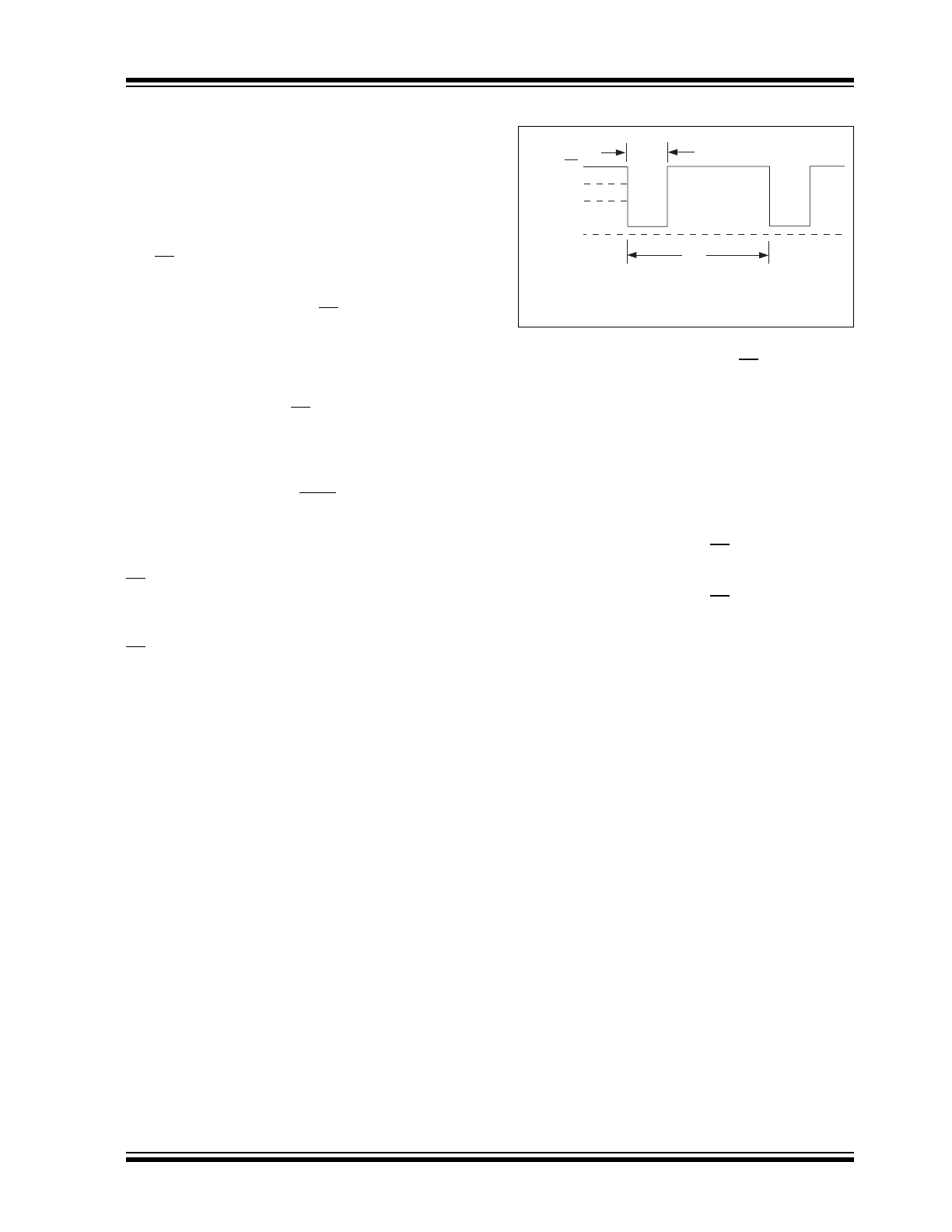
FIGURE 3-1:
Watchdog Strobe
The software routine that drives the RS strobe must be
in a section of the program that executes frequently
enough so the time between toggles is less than one
Watchdog Time-out period. The strobe signal can be
derived from microprocessor address, data and/or
control signals. Typical circuit examples are shown in
Figure .
3.3
Resistor Value Selection
The values of R1 and R2 must be chosen to ensure a
valid low strobe level (V
STL
) on RS when the processor
I/O line is low. The use of 10 k
, ±5% tolerance
resistors are recommended. These values result in a
nominal strobe level of 2.5 on RS (min/max of 2.13V/
3.08V, assuming V
DD
= 5.0V ±10%). Other resistor
values can be used, so long as the additive tolerances
of the power supply and resistor values result in a
strobe that falls within V
STH
and V
STL
under all additive
tolerance conditions.
V
ST
L (Max)
t
ST
t
TD
RS
Note: t
TD
is the maximum elapsed time between strobes which
will keep the watchdog timer from forcing RS LOW.
(A Strobe is defined as a high-to-low transition from V
STH
to V
STL
).
V
STH
(Min)
V
STL
(Min)
TC32M
DS21402D-page 6
2001-2012 Microchip Technology Inc.
3.4
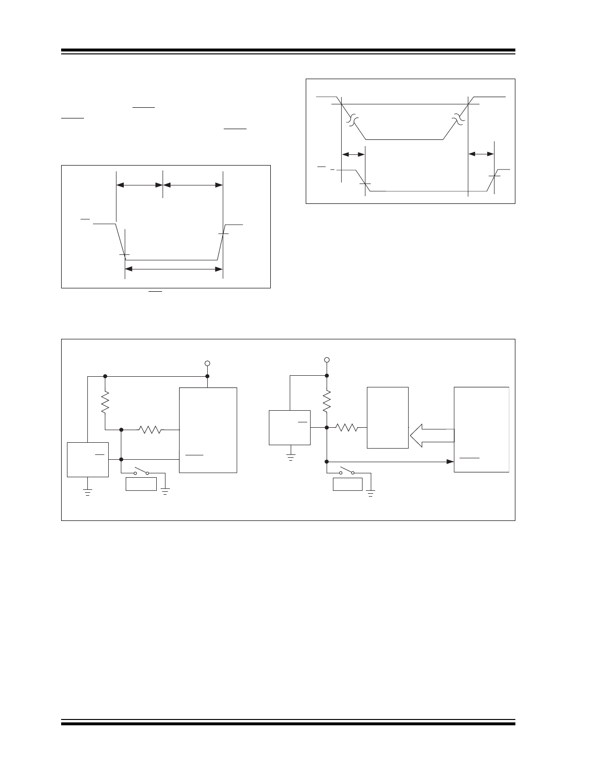
External Override Reset Control
A built-in debounce circuit allows a push-button switch
(PB) or other electronic signal to be wire-ORed to this
pin as an external Reset override control. The external
Reset is required to be an active low signal. Internally,
this input is timed to provide a minimum Reset pulse
width of 500 msec. Reference Figure .
t
FIGURE 3-2:
RS Pulled Low By Push-
Button Reset
FIGURE 3-3:
Power-Up/Down Reset Timing
3.5
Supply Monitor Noise Sensitivity
The TC32M is optimized for fast response to negative-
going changes in V
DD
. Systems with an inordinate
amount of electrical noise on V
DD
(such as systems
using relays), may require a 0.01
F bypass capacitor
to reduce detection sensitivity. This capacitor should be
installed as close to the TC32M as possible to keep the
capacitor lead length short.
FIGURE 3-4:
TC32M Hardware Connections (R1, R2 Chosen To Meet V
STH
, V
STL
)
PB Closed
PB Open
RS
V
IH
t
RST
V
IL
RS
V
IL
V
IH
V
DD
V
RST
t
RST
t
RPD
5V
5V
Reset
PO.1
Reset
Microcontroller
Microprocessor
R2,10 k
Ω
Microcontroller Example
Reset
Decoder
Address
Reset
R1, 10 k
Ω
Microprocessor Example
RS
TC32M
RS
TC32M
R1, 10 k
Ω
R2, 10 k
Ω
2001-2012 Microchip Technology Inc.
DS21402D-page 7
TC32M
4.0
PACKAGING INFORMATION
4.1
Package Marking Information
Package marking data not available at this time.
4.2
Taping Form
Component Taping Orientation for 3-Pin SOT-223 Devices
Package
Carrier Width (W)
Pitch (P)
Part Per Full Reel
Reel Size
3-Pin SOT-223
12 mm
8 mm
4000
13 in
Carrier Tape, Number of Components Per Reel and Reel Size
User Direction of Feed
Device
Marking
Pin 1
Standard Reel Component Orientation
for 713 Suffix Device
(Mark Right Side Up)
W
P
Mark
Face
Component Taping Orientation for 3-Pin TO-92
User Direction of Feed
W
P
Seal
Tape
Back
Tape
M
ARK
F
ACE
M
ARK
F
ACE
M
ARK
F
ACE
TC32M
DS21402D-page 8
2001-2012 Microchip Technology Inc.
4.3
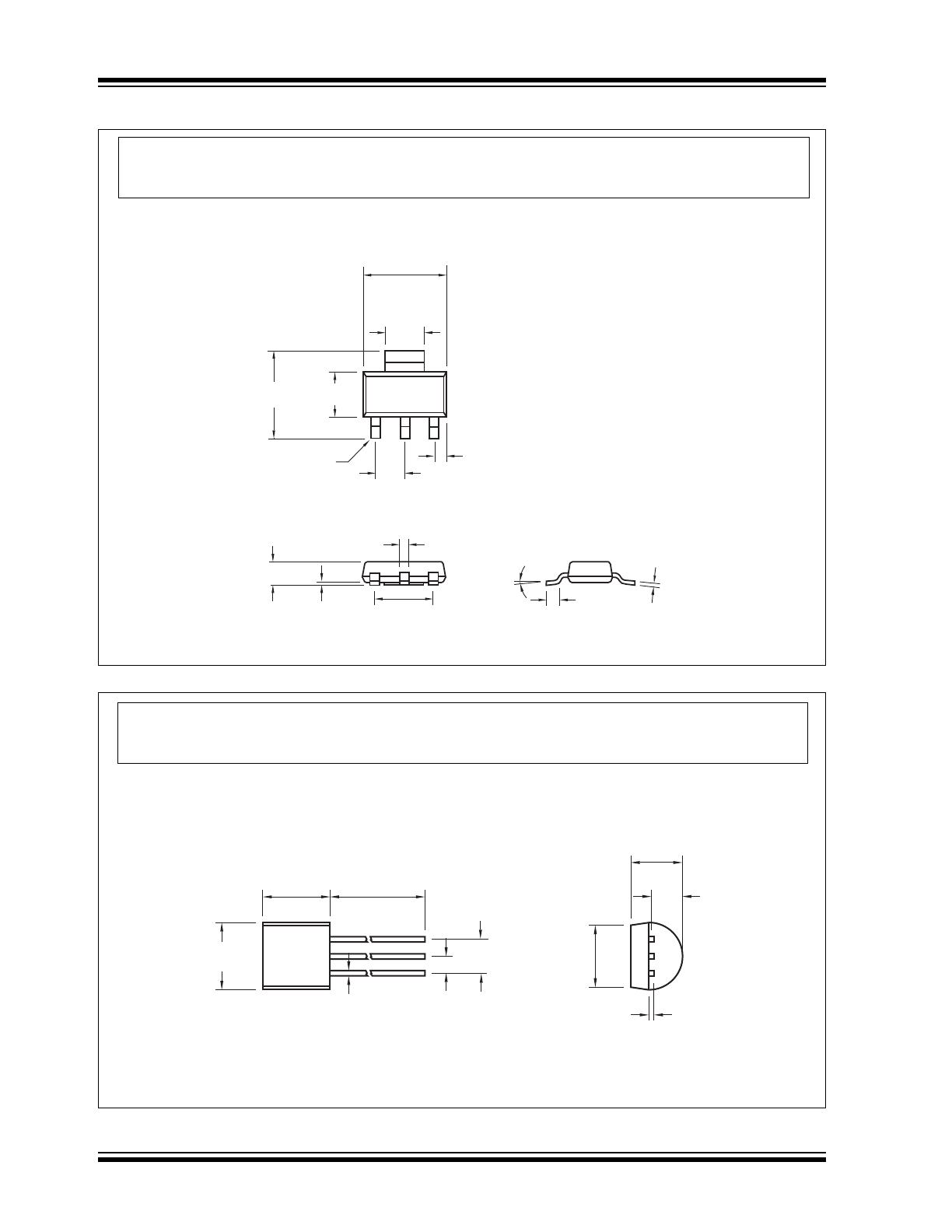
Package Dimensions
.264 (6.70)
.248 (6.30)
.122 (3.10)
.114 (2.90)
.287 (7.30)
.264 (6.70)
.146 (3.70)
.130 (3.30)
.091 (2.30) Typ.
.071
(1.80)
Max.
.181 (4.60) Typ.
.036 (0.91) Min.
.041 (1.04)
.033 (0.84)
Pin 1
.013 (0.33)
.009 (0.24)
.031 (0.80)
.024 (0.60)
.004 (0.10)
.001 (0.02)
10
°
Max.
3-Pin SOT-223
Dimensions: inches (mm)
Note:
For the most current package drawings, please see the Microchip Packaging Specification located
at http://www.microchip.com/packaging
.105 (2.67)
.095 (2.41)
.018 (0.46)
.015 (0.38)
.135
(3.43)
Min.
.500
(12.70)
Min.
.210 (5.33)
.170 (4.32)
.205 (5.21)
.175 (4.45)
.165 (4.19)
.125 (3.18)
.105 (2.67)
.080 (2.03)
.055 (1.40)
.045 (1.14)
.018 (0.46)
.015 (0.38)
TO-92-3
Dimensions: inches (mm)
Note:
For the most current package drawings, please see the Microchip Packaging Specification located
at http://www.microchip.com/packaging

2001-2012 Microchip Technology Inc.
DS21402D-page 9
TC32M
5.0
REVISION HISTORY
Revision D (December 2012)
Added a note to each package outline drawing.

TC32M
DS21402D-page 10
2001-2012 Microchip Technology Inc.
NOTES: