
2001-2012 Microchip Technology Inc.
DS21393D-page 1
TC1426/TC1427/TC1428
Features:
• Low Cost
• Latch-Up Protected: Will Withstand 500 mA
Reverse Output Current
• ESD Protected ±2kV
• High Peak Output Current: 1.2A
• Wide Operating Range:
- 4.5V to 16V
• High Capacitive Load Drive Capability: 1000 pF in
38 nsec
• Low Delay Time: 75 nsec Max
• Logic Input Threshold Independent of Supply
Voltage
• Output Voltage Swing to Within 25 mV of Ground
or V
DD
• Low Output Impedance: 8
Applications:
• Power MOSFET Drivers
• Switched Mode Power Supplies
• Pulse Transformer Drive
• Small Motor Controls
• Print Head Drive
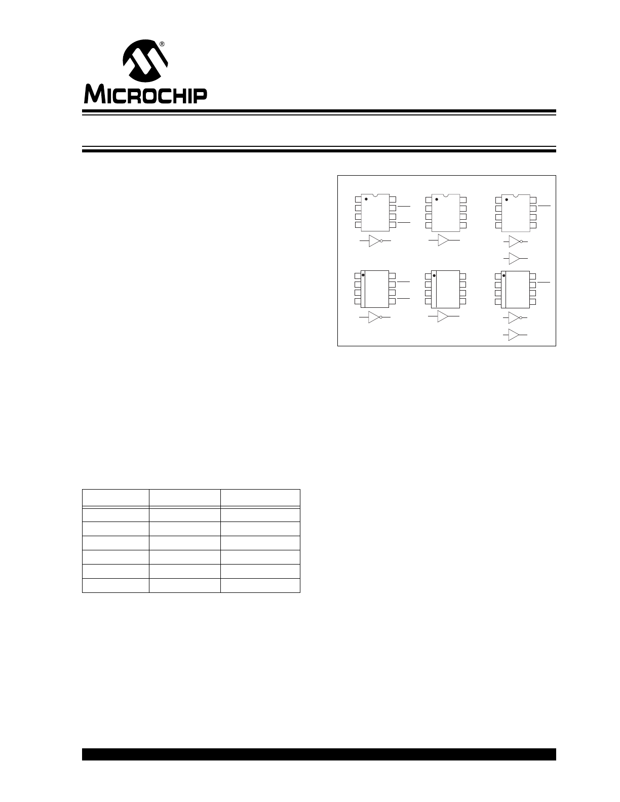
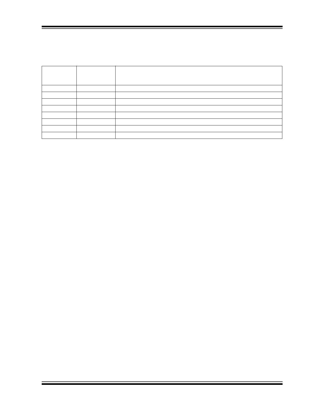
Device Selection Table
Package Type
General Description:
The TC1426/TC1427/TC1428 are a family of 1.2A dual
high-speed drivers. CMOS fabrication is used for low-
power consumption and high efficiency.
These devices are fabricated using an epitaxial layer to
effectively short out the intrinsic parasitic transistor
responsible for CMOS latch-up. They incorporate a
number of other design and process refinements to
increase their long-term reliability.
The TC1426 is compatible with the bipolar DS0026, but
only draws 1/5 of the quiescent current. The TC1426/
TC1427/TC1428 are also compatible with the TC426/
TC427/TC428, but with 1.2A peak output current rather
than the 1.5A of the TC426/TC427/TC428 devices.
Other compatible drivers are the TC4426/TC4427/
TC4428 and the TC4426A/TC4427A/TC4428A. The
TC4426/TC4427/TC4428 have the added feature that
the inputs can withstand negative voltage up to 5V with
diode protection circuits. The TC4426A/TC4427A/
TC4428A have matched input to output leading edge
and falling edge delays, t
D1
and t
D2
, for processing
short duration pulses in the 25 nanoseconds range. All
of the above drivers are pin compatible.
The high-input impedance TC1426/TC1427/TC1428
drivers are CMOS/TTL input-compatible, do not require
the speed-up needed by the bipolar devices, and can
be directly driven by most PWM ICs.
This family of devices is available in inverting and non-
inverting versions. Specifications have been optimized
to achieve low-cost and high-performance devices,
well-suited for the high-volume manufacturer.
Part Number
Package
Temp. Range
TC1426COA
8-Pin SOIC
0°C to +70°C
TC1426CPA
8-Pin PDIP
0°C to +70°C
TC1427COA
8-Pin SOIC
0°C to +70°C
TC1427CPA
8-Pin PDIP
0°C to +70°C
TC1428COA
8-Pin SOIC
0°C to +70°C
TC1428CPA
8-Pin PDIP
0°C to +70°C
TC1426CPA
1
2
3
4
NC
5
6
7
8
OUT A
OUT B
NC
IN A
GND
IN B
V
DD
2, 4
7, 5
Inverting
TC1427CPA
1
2
3
4
NC
5
6
7
8
OUT A
OUT B
NC
IN A
GND
IN B
2, 4
7, 5
Noninverting
TC1428CPA
1
2
3
4
NC
5
6
7
8
OUT A
OUT B
NC
IN A
GND
IN B
2
7
4
5
V
DD
V
DD
TC1426COA
1
2
3
4
NC
5
6
7
8
OUT A
OUT B
NC
IN A
GND
IN B
V
DD
NC = No connection
2, 4
7, 5
Inverting
TC1427COA
1
2
3
4
NC
5
6
7
8
OUT A
OUT B
NC
IN A
GND
IN B
2, 4
7, 5
Noninverting
TC1428COA
1
2
3
4
NC
5
6
7
8
OUT A
OUT B
NC
IN A
GND
IN B
2
7
4
5
V
DD
V
DD
8-Pin PDIP/SOIC
1.2A Dual High-Speed MOSFET Drivers
TC1426/TC1427/TC1428
DS21393D-page 2
2001-2012 Microchip Technology Inc.
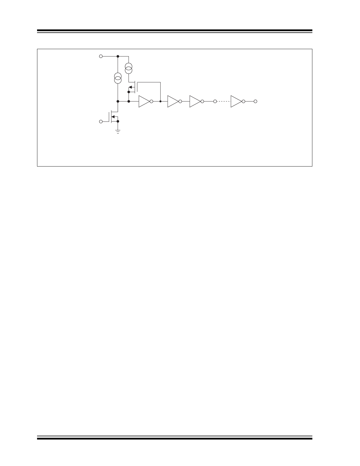
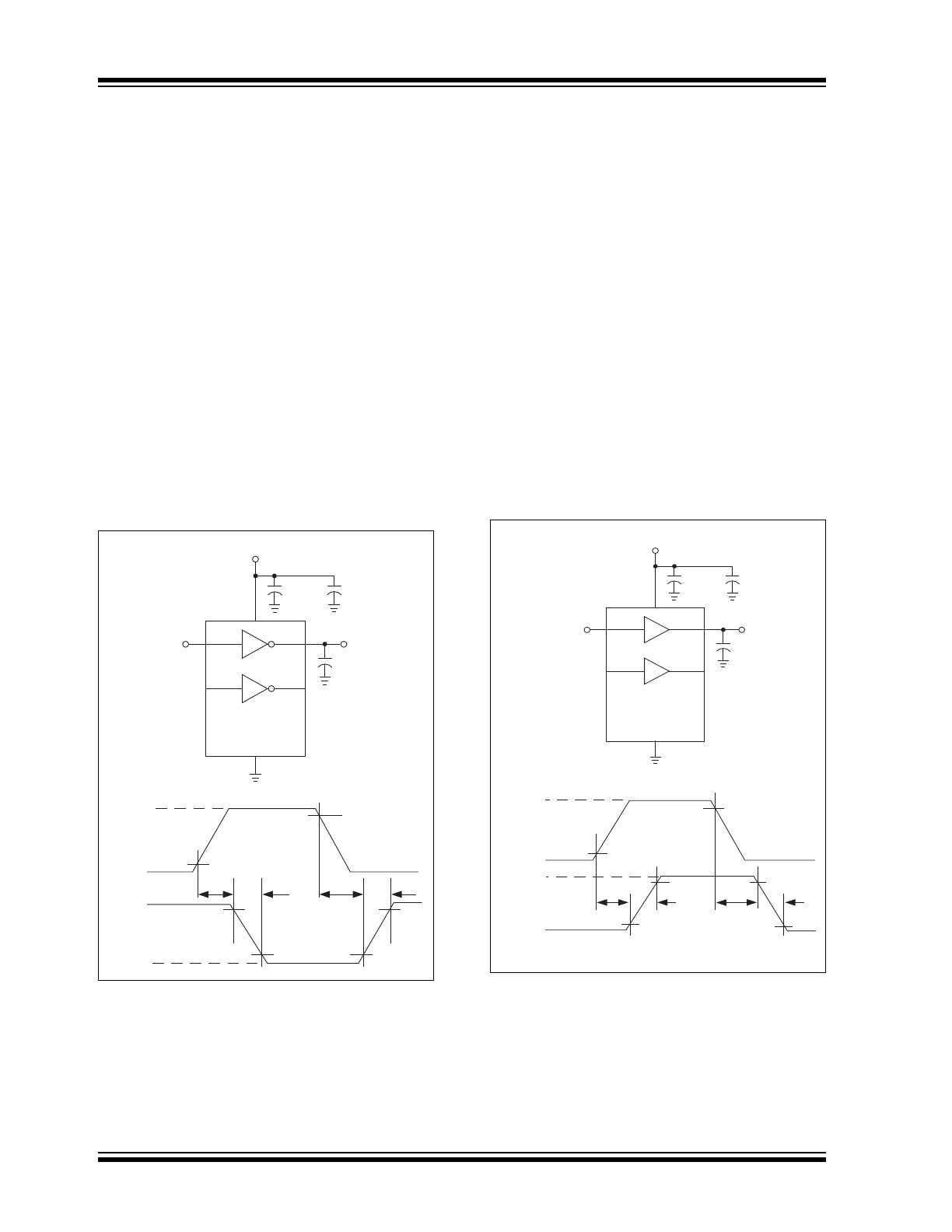
Functional Block Diagram
Input
V+
≈2.5
μA
≈500
μA
NOTE: TC1428 has one inverting and one noninverting driver.
Ground any unused driver input.
Inverting
Output
Noninverting
Output
(TC1426)
(TC1427)
GND
TC1426 Inverting
TC1427 Noninverting
TC1428 Inverting/Noninverting
2001-2012 Microchip Technology Inc.
DS21393D-page 3
TC1426/TC1427/TC1428
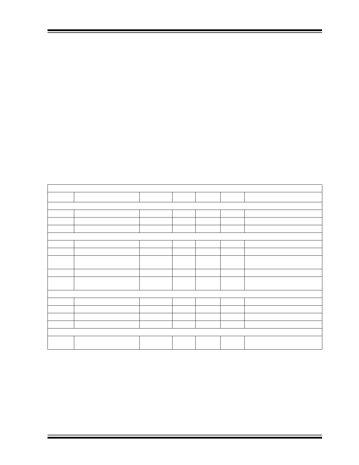
1.0
ELECTRICAL
CHARACTERISTICS
Absolute Maximum Ratings*
Supply Voltage ..................................................... +18V
Input Voltage, Any Terminal
................................... V
DD
+ 0.3V to GND – 0.3V
Power Dissipation (T
A
70°C)
PDIP........................................................ 730 mW
SOIC ....................................................... 470 mW
Derating Factor
PDIP....................................................... 8 mW/
C
SOIC ...................................................... 4 mW/
C
Operating Temperature Range
C Version ........................................ 0°C to +70°C
Storage Temperature Range .............. -65°C to +150°C
*Stresses above those listed under "Absolute
Maximum Ratings" may cause permanent damage to
the device. These are stress ratings only and functional
operation of the device at these or any other conditions
above those indicated in the operation sections of the
specifications is not implied. Exposure to Absolute
Maximum Rating conditions for extended periods may
affect device reliability.
TC1426/TC1427/TC1428 ELECTRICAL SPECIFICATIONS
Electrical Characteristics: T
A
= +25°C, with 4.5V
V
DD
16V, unless otherwise noted.
Symbol
Parameter
Min
Typ
Max
Units
Test Conditions
Input
V
IH
Logic 1, High Input Voltage
3
—
—
V
V
IL
Logic 0, Low Input Voltage
—
—
0.8
V
I
IN
Input Current
-1
—
1
A
0V
V
IN
V
DD
Output
V
OH
High Output Voltage
V
DD
– 0.025
—
—
V
Figure 3-1, Figure 3-2
V
OL
Low Output Voltage
—
—
0.025
V
Figure 3-1, Figure 3-2
R
O
Output Resistance
—
—
12
8
18
12
I
OUT
= 10 mA, V
DD
= 16V
I
PK
Peak Output Current
—
1.2
—
A
I
REV
Latch-Up Current
Withstand Reverse Current
—
>500
—
mA
Switching Time (Note 1)
t
R
Rise Time
—
—
35
nsec
Figure 3-1, Figure 3-2
t
F
Fall Time
—
—
25
nsec
Figure 3-1, Figure 3-2
t
D1
Delay Time
—
—
75
nsec
Figure 3-1, Figure 3-2
t
D2
Delay Time
—
—
75
nsec
Figure 3-1, Figure 3-2
Power Supply
I
S
Power Supply Current
—
—
—
—
9
0.5
mA
V
IN
= 3V (Both Inputs)
V
IN
= 0V (Both Inputs)
Note
1:
Switching times ensured by design.
TC1426/TC1427/TC1428
DS21393D-page 4
2001-2012 Microchip Technology Inc.
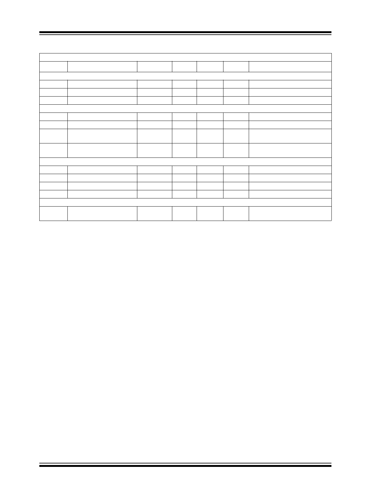
TC1426/TC1427/TC1428 ELECTRICAL SPECIFICATIONS (CONTINUED)
Electrical Characteristics: Over operating temperature range with 4.5V
V
DD
16V, unless otherwise noted.
Symbol
Parameter
Min
Typ
Max
Units
Test Conditions
Input
V
IH
Logic 1, High Input Voltage
3
—
—
V
V
IL
Logic 0, Low Input Voltage
—
—
0.8
V
I
IN
Input Current
-10
—
10
A
0V
V
IN
V
DD
Output
V
OH
High Output Voltage
V
DD
– 0.025
—
—
V
Figure 3-1, Figure 3-2
V
OL
Low Output Voltage
—
—
0.025
V
Figure 3-1, Figure 3-2
R
O
Output Resistance
—
—
15
10
23
18
I
OUT
= 10 mA, V
DD
= 16V
I
REV
Latch-Up Current
Withstand Reverse Current
—
>500
—
mA
Switching Time (Note 1)
t
R
Rise Time
—
—
60
nsec
Figure 3-1, Figure 3-2
t
F
Fall Time
—
—
40
nsec
Figure 3-1, Figure 3-2
t
D1
Delay Time
—
—
125
nsec
Figure 3-1, Figure 3-2
t
D2
Delay Time
—
—
125
nsec
Figure 3-1, Figure 3-2
Power Supply
I
S
Power Supply Current
—
—
—
—
13
0.7
mA
V
IN
= 3V (Both Inputs)
V
IN
= 0V (Both Inputs)
Note
1:
Switching times ensured by design.
2001-2012 Microchip Technology Inc.
DS21393D-page 5
TC1426/TC1427/TC1428
2.0
PIN DESCRIPTIONS
The descriptions of the pins are listed in Table 2-1.
TABLE 2-1:
PIN FUNCTION TABLE
Pin No.
(8-Pin PDIP,
SOIC)
Symbol
Description
1
NC
No connection.
2
IN A
Control input A, TTL/CMOS compatible logic input.
3
GND
Ground.
4
IN B
Control input B, TTL/CMOS compatible logic input.
5
OUT B
Output B, CMOS totem-pole output.
6
V
DD
Supply input, 4.5V to 16V.
7
OUT A
Output A, CMOS totem-pole output.
8
NC
No connection.
TC1426/TC1427/TC1428
DS21393D-page 6
2001-2012 Microchip Technology Inc.
3.0
APPLICATIONS INFORMATION
3.1
SUPPLY BYPASSING
Large currents are required to charge and discharge
capacitive loads quickly. For example, charging a 1000
pF load to 16V in 25 nsec requires a 0.8A current from
the device's power supply.
To ensure low supply impedance over a wide frequency
range, a parallel capacitor combination is recom-
mended for supply bypassing. Low-inductance ceramic
MLC capacitors with short lead lengths (<0.5-in.)
should be used. A 1.0
F film capacitor in parallel with
one or two 0.1
F ceramic MLC capacitors normally
provides adequate bypassing.
3.2
GROUNDING
The TC1426 and TC1428 contain inverting drivers.
Individual ground returns for the input and output
circuits or a ground plane should be used. This will
reduce negative feedback that causes degradation in
switching speed characteristics.
FIGURE 3-1:
Inverting Driver Switching
Time
3.3
INPUT STAGE
The input voltage level changes the no-load or
quiescent supply current. The N-channel MOSFET
input stage transistor drives a 2.5 mA current source
load. With a logic ‘1’ input, the maximum quiescent
supply current is 9 mA. Logic ‘0’ input level signals
reduce quiescent current to 500
A maximum. Unused
driver inputs must be connected to V
DD
or GND.
Minimum power dissipation occurs for logic ‘0’ inputs
for the TC1426/TC1427/TC1428.
The drivers are designed with 100 mV of hysteresis.
This provides clean transitions and minimizes output
stage current spiking when changing states. Input
voltage thresholds are approximately 1.5V, making a
logic ‘1’ input any voltage greater than 1.5V up to V
DD
.
Input current is less than 1
A over this range.
The TC1426/TC1427/TC1428 may be directly driven
by the TL494, SG1526/27, TC38C42, TC170 and
similar switch-mode power supply integrated circuits.
FIGURE 3-2:
Noninverting Driver
Switching Time
+5V
10%
90%
10%
90%
10%
90%
V
DD
1
μF
WIMA
MKS-2
0V
0V
TC1426
(1/2 TC1428)
1
2
Test Circuit
0.1
μF MLC
Input
V
DD
= 16V
Output
t
R
C
L
= 1000 pF
t
D1
t
F
t
D2
Input
Output
V
DD
0.1
μF MLC
Input
V
DD
= 16V
Output
t
R
C
L
= 1000 pF
t
D1
t
F
t
D2
Input
Output
90%
10%
10%
10%
90%
1
μF
WIMA
MKS-2
TC1427
(1/2 TC1428)
+5V
0V
0V
90%
Test Circuit
1
2
2001-2012 Microchip Technology Inc.
DS21393D-page 7
TC1426/TC1427/TC1428
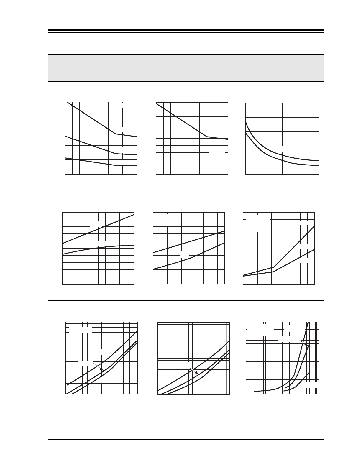
4.0
TYPICAL CHARACTERISTICS
Note:
The graphs and tables provided following this note are a statistical summary based on a limited number of
samples and are provided for informational purposes only. The performance characteristics listed herein
are not tested or guaranteed. In some graphs or tables, the data presented may be outside the specified
operating range (e.g., outside specified power supply range) and therefore outside the warranted range.
550
440
330
220
110
0
5
7
9
11
13
15
TIME (nsec)
V
DD
(V)
10,000 pF
4700 pF
2200 pF
Rise Time vs. Supply Voltage
330
264
198
132
66
0
TIME (nsec)
10,000 pF
2200 pF
4700 pF
5
7
9
11
13
15
Fall Time vs. Supply Voltage
t
D1
TIME (nsec)
5
7
9
11
13
15
80
70
60
50
40
30
Delay Time vs. Supply Voltage
T
A
= +25°C
T
A
= +25°C
C
L
= 1000 pF
T
A
= +25°C
V
DD
(V)
V
DD
(V)
t
D2
40
32
24
16
8
0
25
45
65
85
105
125
TEMPERATURE (
°C)
TIME (nsec)
Rise and Fall Times vs. Temperature
60
54
48
42
36
0
25
45
65
85
105
125
TEMPERATURE (
°C)
TIME (nsec)
Delay Time vs. Temperature
30
24
18
12
6
0
100
520
940
1360
1780
2200
SUPPL
Y
CURRENT (mA)
CAPACITIVE LOAD (pF)
500 kHz
200 kHz
20 kHz
Supply Current vs. Capacitive Load
C
L
= 1000 pF
V
DD
= +15V
T
A
= +25°C
C
L
= 1000 pF
V
DD
= +15V
C
L
= 1000 pF
V
DD
= +15V
t
D1
t
D2
t
FALL
t
RISE
CAPACITIVE LOAD (pF)
100
1000
10,000
1000
100
10
10 V
DD
TIME (nsec)
5 V
DD
15 V
DD
Rise Time vs. Capacitive Load
1000
100
10
100
1000
10,000
CAPACITIVE LOAD (pF)
TIME (nsec)
5 V
DD
10 V
DD
Fall Time vs. Capacitive Load
15V
DD
100
80
60
40
20
0
10
100
1000
10,000
V
DD
= 15V
V
DD
= 10V
V = 5V
DD
FREQUENCY (kHz)
SUPPL
Y
CURRENT (mA)
Supply Current vs. Frequency
C
L
= 1000 pF
T
A
= +25°C
T
A
= +25°C
T
A
= +25°C
TC1426/TC1427/TC1428
DS21393D-page 8
2001-2012 Microchip Technology Inc.
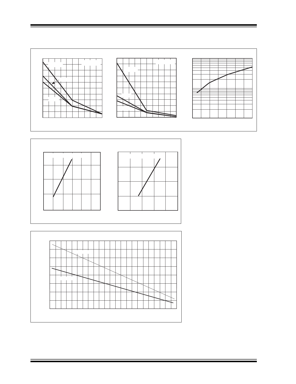
TYPICAL CHARACTERISTICS (CONTINUED)
100 mA
50 mA
10 mA
15
13
11
9
7
5
5
7
9
11
13
15
OUT
(Ω)
R
Low-State Output Resistance
50
42
34
26
18
10
5
7
9
11
13
15
100 mA
50 mA
10 mA
High-State Output Resistance
R
OUT
(Ω
)
10
-8
A
(sec)
10
-9
10
-10
4
6
8
10
12
14
16
18
Crossover Energy Loss
T
A
= +25°C
T
A
= +25°C
V
DD
(V)
V
DD
(V)
V
DD
(V)
20
15
10
5
0
0
50
100
150
200
300
400
S
UPPL
Y
VOL
T
AGE (V)
SUPPLY CURRENT (
μA)
Quiescent Power Supply
Current vs. Supply Voltage
BOTH INPUTS LOGIC ‘
0’
20
15
10
5
0
1
2
3
4
5
6
SUPPL
Y
VOL
T
AGE (V)
SUPPLY CURRENT (mA)
BOTH INPUTS LOGIC ‘
1’
Quiescent Power Supply
Current vs. Supply Voltage
200
0
400
600
800
1000
1200
1400
1600
0
10
20
30
40
50
60
70
80
90
100
110
120
AMBIENT TEMPERATURE (°C)
MAX. POWER (mW)
8 Pin DIP
Thermal Derating Curves
8 Pin SOIC
2001-2012 Microchip Technology Inc.
DS21393D-page 9
TC1426/TC1427/TC1428
5.0
PACKAGING INFORMATION
5.1
Package Marking Information
Package marking data not available at this time.
5.2
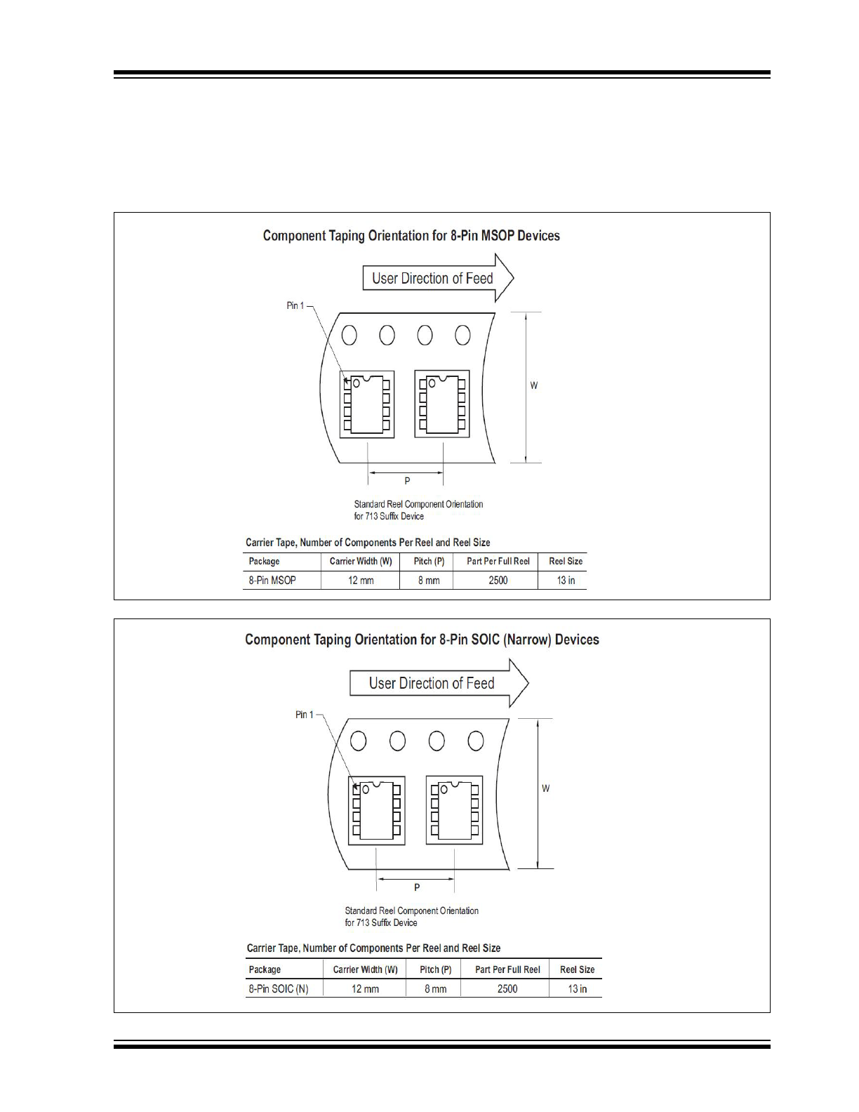
Taping Form
TC1426/TC1427/TC1428
DS21393D-page 10
2001-2012 Microchip Technology Inc.
5.3
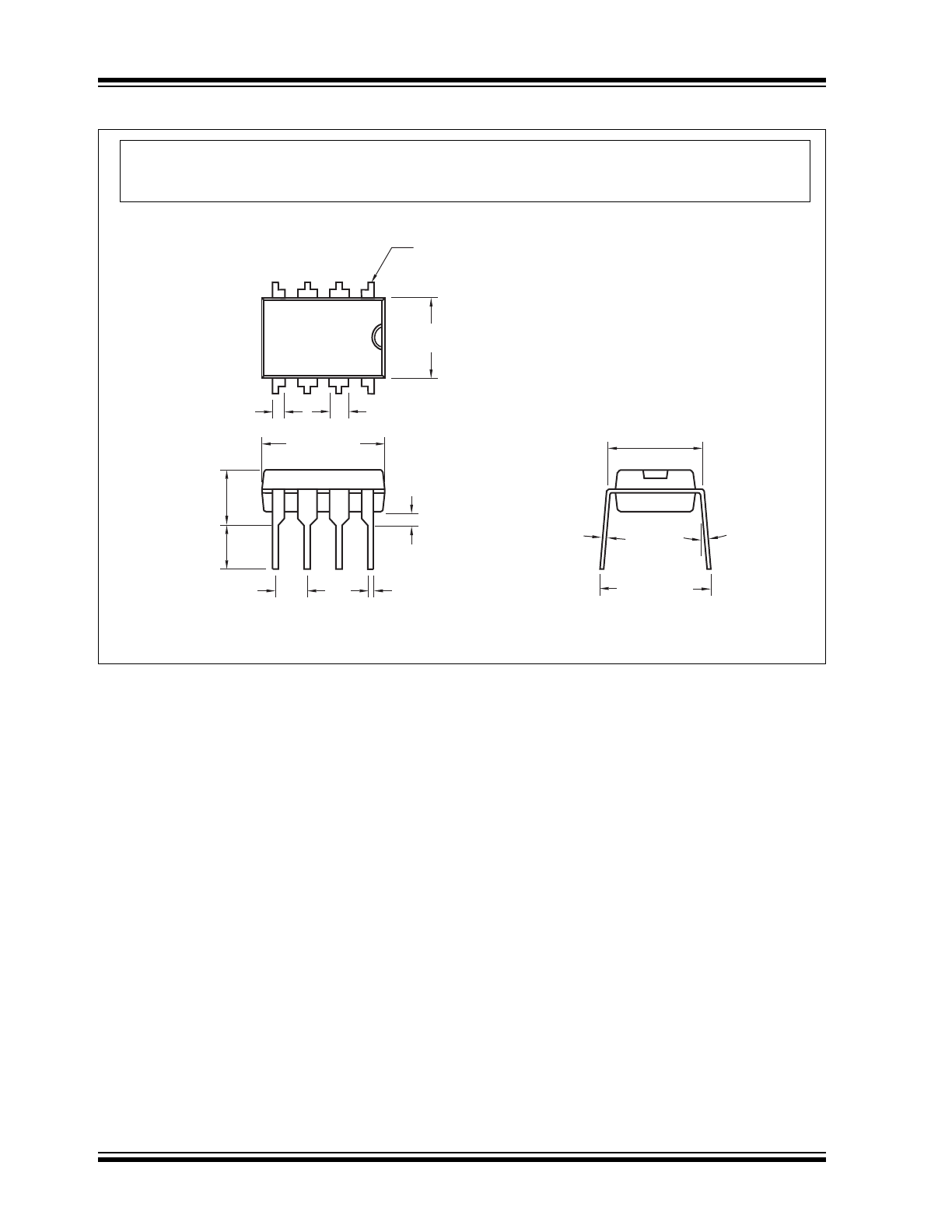
Package Dimensions
3° Min.
Pin 1
.260 (6.60)
.240 (6.10)
.045 (1.14)
.030 (0.76)
.070 (1.78)
.040 (1.02)
.400 (10.16)
.348 (8.84)
.200 (5.08)
.140 (3.56)
.150 (3.81)
.115 (2.92)
.110 (2.79)
.090 (2.29)
.022 (0.56)
.015 (0.38)
.040 (1.02)
.020 (0.51)
.015 (0.38)
.008 (0.20)
.310 (7.87)
.290 (7.37)
.400 (10.16)
.310 (7.87)
8-Pin Plastic DIP
Dimensions: inches (mm)
Note:
For the most current package drawings, please see the Microchip Packaging Specification located
at http://www.microchip.com/packaging