
2002-2012 Microchip Technology Inc.
DS21386C-page 1
TC1320
Features
• 8-bit Digital-to-Analog Converter
• ±2 LSB INL
• ±0.8 LSB DNL
• 2.7-5.5V Single Supply Operation
• Simple SMBus/I
2
C
TM
Serial Interface
• Low Power: 350
A Operation, 0.5A Shutdown
• 8-Pin SOIC and 8-Pin MSOP Packages
Applications
• Programmable Voltage Sources
• Digital Controlled Amplifiers/Attenuators
• Process Monitoring and Control
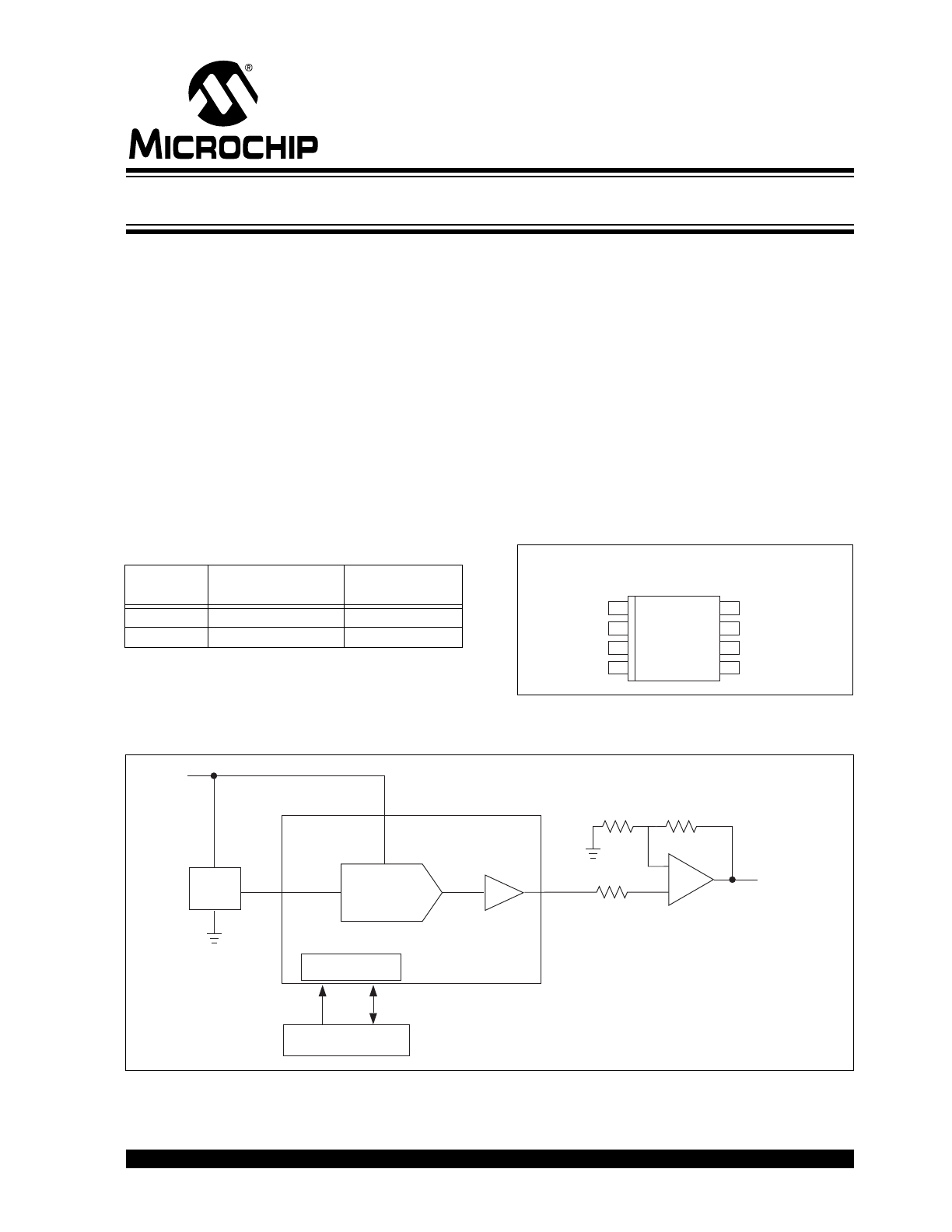
Device Selection Table
General Description
The TC1320 is a serially accessible 8-bit voltage output
digital-to-analog converter (DAC). The DAC produces
an output voltage that ranges from ground to an exter-
nally supplied reference voltage. It operates from a sin-
gle power supply that can range from 2.7V to 5.5V,
making it ideal for a wide range of applications. Built
into the part is a Power-on Reset function that ensures
that the device starts at a known condition.
Communication with the TC1320 is accomplished via a
simple 2-wire SMBus/I
2
C™ compatible serial port with
the TC1320 acting as a slave only device. The host can
enable the SHDN bit in the CONFIG register to activate
the Low Power Standby mode.
Package Type
Typical Application
Part
Number
Package
Temperature
Range
TC1320EOA
8-Pin SOIC (Narrow)
-40°C to +85°C
TC1320EUA
8-Pin MSOP
-40°C to +85°C
GND
SDA
V
REF
SCL
NC
V
OUT
V
DD
DAC-OUT
1
8
2
7
3
6
4
5
TC1320
8-Pin MSOP and
8-Pin SOIC (Narrow)
Microcontroller
Serial Port
SDAT
SCLK
V
IN
VADJUST
V
DD
(1)
(8)
(3)
(2)
DAC
V
REF
(5)
V
OUT
TC1320
+
–
(2)
8-Bit Digital-to-Analog Converter with Two-Wire Interface
TC1320
DS21386C-page 2
2002-2012 Microchip Technology Inc.
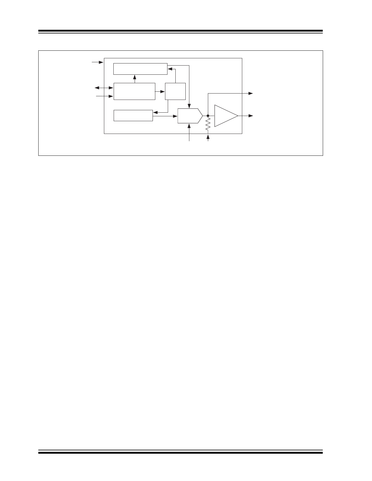
Functional Block Diagram
Serial Port
Interface
SDA
V
DD
DAC-OUT
V
OUT
Configuration Register
Data Register
Control
V
REF
GND
SCL
DAC
TC1320
2002-2012 Microchip Technology Inc.
DS21386C-page 3
TC1320
1.0
ELECTRICAL
CHARACTERISTICS
Absolute Maximum Ratings*
Supply Voltage (V
DD
) ............................................. +6V
Voltage on any Pin .. (GND – 0.3V) to (V
DD
+ 0.3V)
Current on any Pin ............................................ ±50mA
Package Thermal Resistance (
JA
)............ 330°C C/W
Operating Temperature (T
A
)........................ See Below
Storage Temperature (T
STG
) .............. -65°C to +150°C
*Stresses above those listed under "Absolute Maximum
Ratings" may cause permanent damage to the device. These
are stress ratings only and functional operation of the device
at these or any other conditions above those indicated in the
operation sections of the specifications is not implied.
Exposure to Absolute Maximum Rating conditions for
extended periods may affect device reliability.
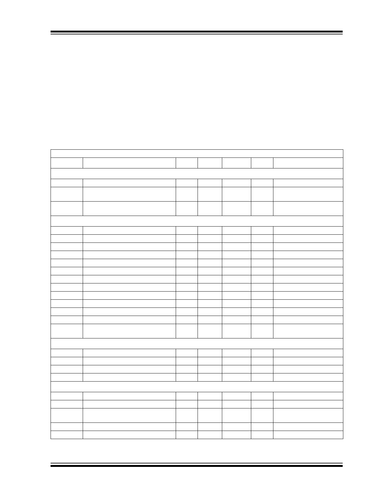
TC1320 ELECTRICAL SPECIFICATIONS
Electrical Characteristics: V
DD
= 2.7V to 5.5V, -40°C
T
A
+85°C, V
REF
= 1.2V unless otherwise noted.
Symbol
Parameter
Min
Typ
Max
Unit
Test Conditions
Power Supply
V
DD
Supply Voltage
2.7
350
500
A
I
DD
Operating Current
—
0.35
0.5
mA
V
DD
= 5.5V, V
REF
= 1.2V
Serial Port Inactive (Note 1)
I
DD-STANDBY
Standby Supply Current
—
0.1
1
A
V
DD
= 3.3V
Serial Port Inactive (Note 1)
Static Performance - Analog Section
Resolution
—
—
8
Bits
INL
Integral Non-Linearity at FS, T
A
= +25°C
—
—
±2
LSB
(Note 2)
FSE
Full Scale Error
—
—
±3
%FS
DNL
Differential Non-Linearity, T
A
= +25°C
—
—
±0.8
LSB
All Codes (Note 2)
V
OS
Offset Error at V
OUT
—
±0.3
±8
mV
(Note 2)
TCV
OS
Offset Error Tempco at V
OUT
—
10
—
v/°C
PSRR
Power Supply Rejection Ratio
—
80
—
dB
V
DD
at DC
V
REF
Voltage Reference Range
0
—
V
DD
– 1.2
V
I
REF
Reference Input Leakage Current
—
—
±1.0
A
V
SW
Voltage Swing
0
—
V
REF
V
V
REF
(V
DD
– 1.2V)
R
OUT
Output Resistance @ V
OUT
—
5
—
R
OUT
(
)
I
OUT
Output Current (Source or Sink)
—
2
—
mA
I
SC
Output Short-Circuit Current
V
DD
= 5.5V
—
—
30
20
50
50
mA
mA
Source
Sink
Dynamic Performance
SR
Voltage Output Slew Rate
—
0.8
—
V/
s
t
SETTLE
Output Voltage Full Scale Settling Time
—
10
—
sec
t
WU
Wake-up Time
—
20
—
s
Digital Feed Through and Crosstalk
—
5
—
nV-s
SDA = V
DD
, SCL = 100kHz
Serial Port Interface
V
IH
Logic Input High
2.4
—
V
DD
V
V
IL
Logic Input Low
—
—
0.6
—
V
OL
SDA Output Low
—
—
—
—
0.4
0.6
V
V
I
OL
= 3mA (Sinking Current)
I
OL
= 6mA
C
IN
Input Capacitance SDA, SCL
—
5
0.4
pF
I
LEAK
I/O Leakage
—
—
±1.0
A
Note
1: SDA and SCL must be connected to V
DD
or GND.
2: Measured at V
OUT
50mV referred to GND to avoid output buffer clipping.
TC1320
DS21386C-page 4
2002-2012 Microchip Technology Inc.
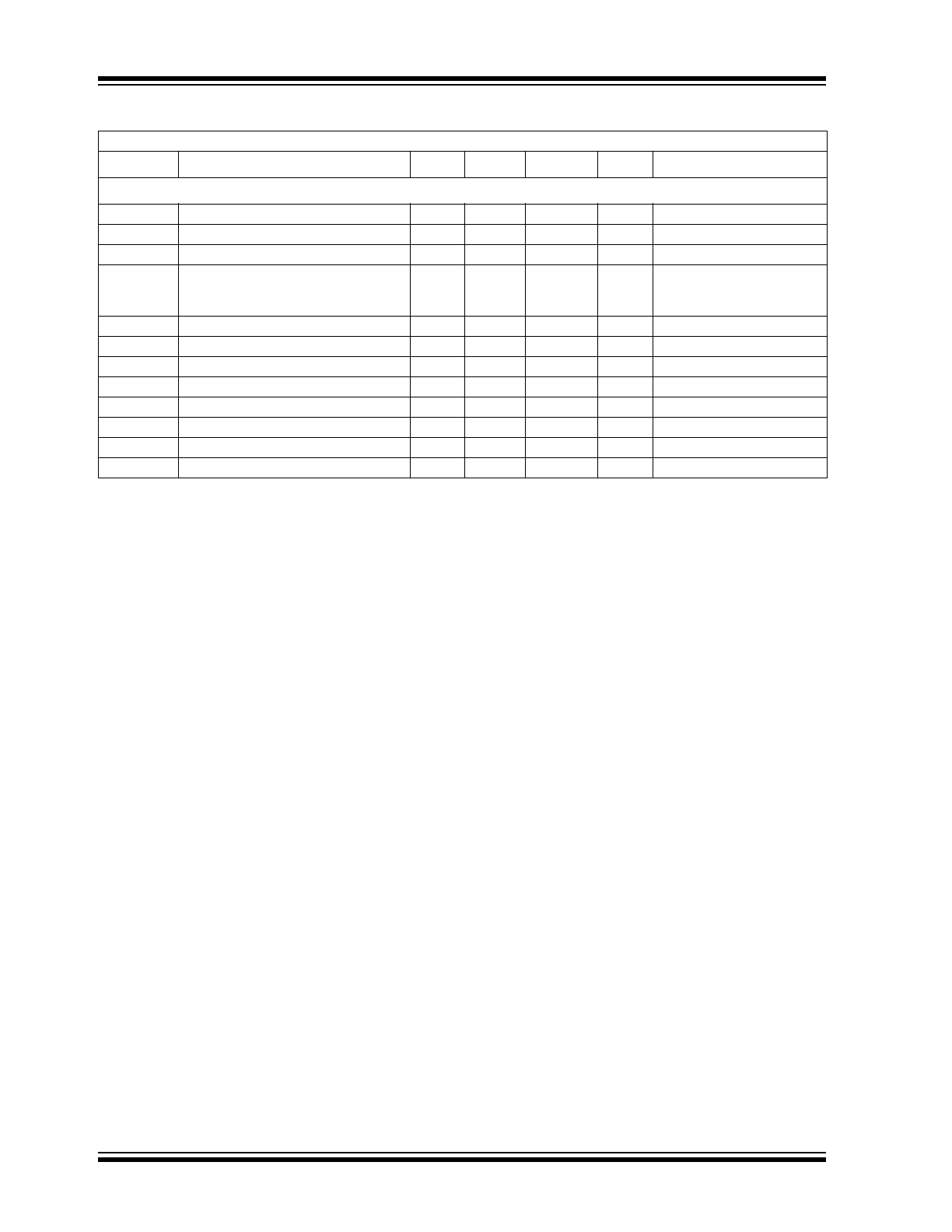
Serial Port AC Timing
f
SMB
SMBus Clock Frequency
10
—
100
kHz
t
IDLE
Bus Free Time Prior to New Transition
4.7
—
—
sec
t
H(START)
START Condition Hold Time
4.0
—
—
sec
t
SU(START)
START Condition Setup Time
4.7
—
—
sec
90% SCL to 10% SDA
(for Repeated START
Condition)
t
SU(STOP)
STOP Condition Setup Time
4.0
—
—
sec
t
H-DATA
Data In Hold Time
100
—
—
nsec
t
SU-DATA
Data In Setup Time
100
—
—
nsec
t
LOW
Low Clock Period
4.7
—
—
sec
10% to 10%
t
HIGH
High Clock Period
4
—
—
sec
90% to 90%
t
F
SMBus Fall Time
—
—
300
nsec
90% to 10%
t
R
SMBus Rise Time
—
—
1000
nsec
10% to 90%
t
POR
Power-on Reset Delay
—
500
—
sec
V
DD
V
POR
(Rising Edge)
TC1320 ELECTRICAL SPECIFICATIONS (CONTINUED)
Electrical Characteristics: V
DD
= 2.7V to 5.5V, -40°C
T
A
+85°C, V
REF
= 1.2V unless otherwise noted.
Symbol
Parameter
Min
Typ
Max
Unit
Test Conditions
Note
1: SDA and SCL must be connected to V
DD
or GND.
2: Measured at V
OUT
50mV referred to GND to avoid output buffer clipping.
2002-2012 Microchip Technology Inc.
DS21386C-page 5
TC1320
2.0
PIN DESCRIPTIONS
The descriptions of the pins are listed in Table 2-1.
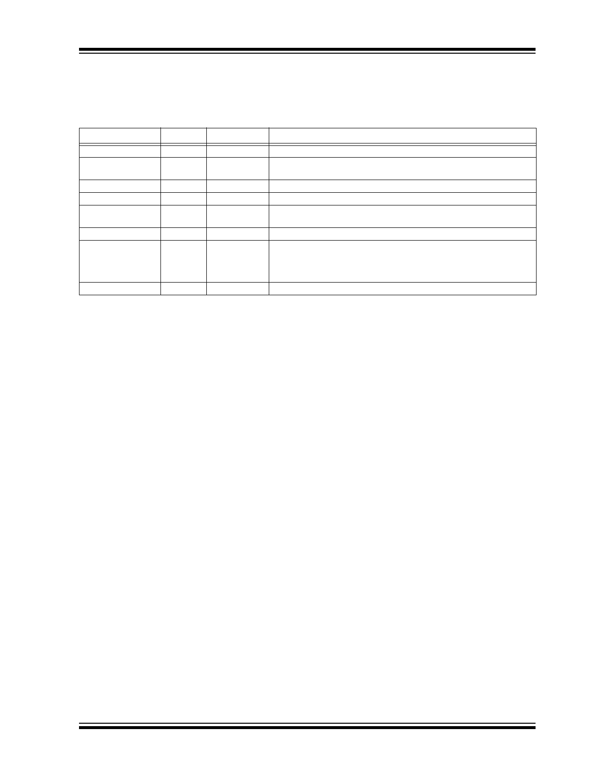
TABLE 2-1:
PIN FUNCTION TABLE
Pin Number
Symbol
Type
Description
1
V
REF
Input
Input. Voltage Reference Input can range from 0V to 1.2V below V
DD
.
2 SDA
Bi-Directional
Bi-directional.
Serial
data
is transferred on the SMBus in both directions
using this pin.
3
SCL
Input
Input. SMBus serial clock. Clocks data into and out of the TC1320.
4
GND
Power
Ground.
5
V
OUT
Output
Output. Buffered DAC output voltage. This voltage is a function of the
reference voltage and the contents of the DATA register.
6
NC
None
No connection.
7
DAC-OUT
Output
Output. Unbuffered DAC output voltage. This voltage is a function of the
reference voltage and the contents of the DATA register. This output is
unbuffered and care must be taken that the pin is connected only to a
high-impedance node.
8
V
DD
Power
Positive power supply input. See electrical specifications.
TC1320
DS21386C-page 6
2002-2012 Microchip Technology Inc.
3.0
DETAILED DESCRIPTION
The TC1320 is a monolithic 8-bit digital-to-analog con-
verter, that is designed to operate from a single supply
that can range from 2.7V to 5.5V. The DAC consists of
a data register (DATA), a configuration register
(CONF), and a current output amplifier. The TC1320
uses an external reference, which also determines the
maximum output voltage.
The TC1320 uses a current steering DAC, based on an
array of matched current sources. This current, along a
precision resistor, converts the contents of the Data
Register and V
REF
into an output voltage, V
OUT
given
by:
V
OUT
= V
REF
(DATA/256)
3.1
Reference Input
The reference pin, V
REF
, is a buffered high-impedance
input and because of this, the load regulation of the ref-
erence source needs only to be able to tolerate leakage
levels of current (less than 1
A). V
REF
accepts a volt-
age range from 0 to (V
DD
– 1.2V). Input capacitance is
typically 10pF.
3.2
Output Amplifier
The TC1320 DAC output is buffered with an internal
unity gain rail-to-rail input/output amplifier, with a typical
slew rate of 0.8V/
sec. Maximum full scale transition
settling time is 10
sec to within ±1/2LSB when loaded
with 1k
in parallel with 100pF.
3.3
Standby Mode
The TC1320 allows the host to put it into a Low Power
(I
DD
= 0.5
A, typical) Standby mode. In this mode, the
D/A conversion is halted. The SMBus port operates
normally. Standby mode is enabled by setting the
SHDN bit in the CONFIG register. The table below
summarizes this operation.
TABLE 3-1:
STANDBY MODE OPERATION
3.4
SMBus Slave Address
The TC1320 is internally programmed to have a default
SMBus address value of 1001 000b. Seven other
addresses are available by custom order (contact fac-
tory). See Figure 3-1 for locating address bits in SMBus
protocol.
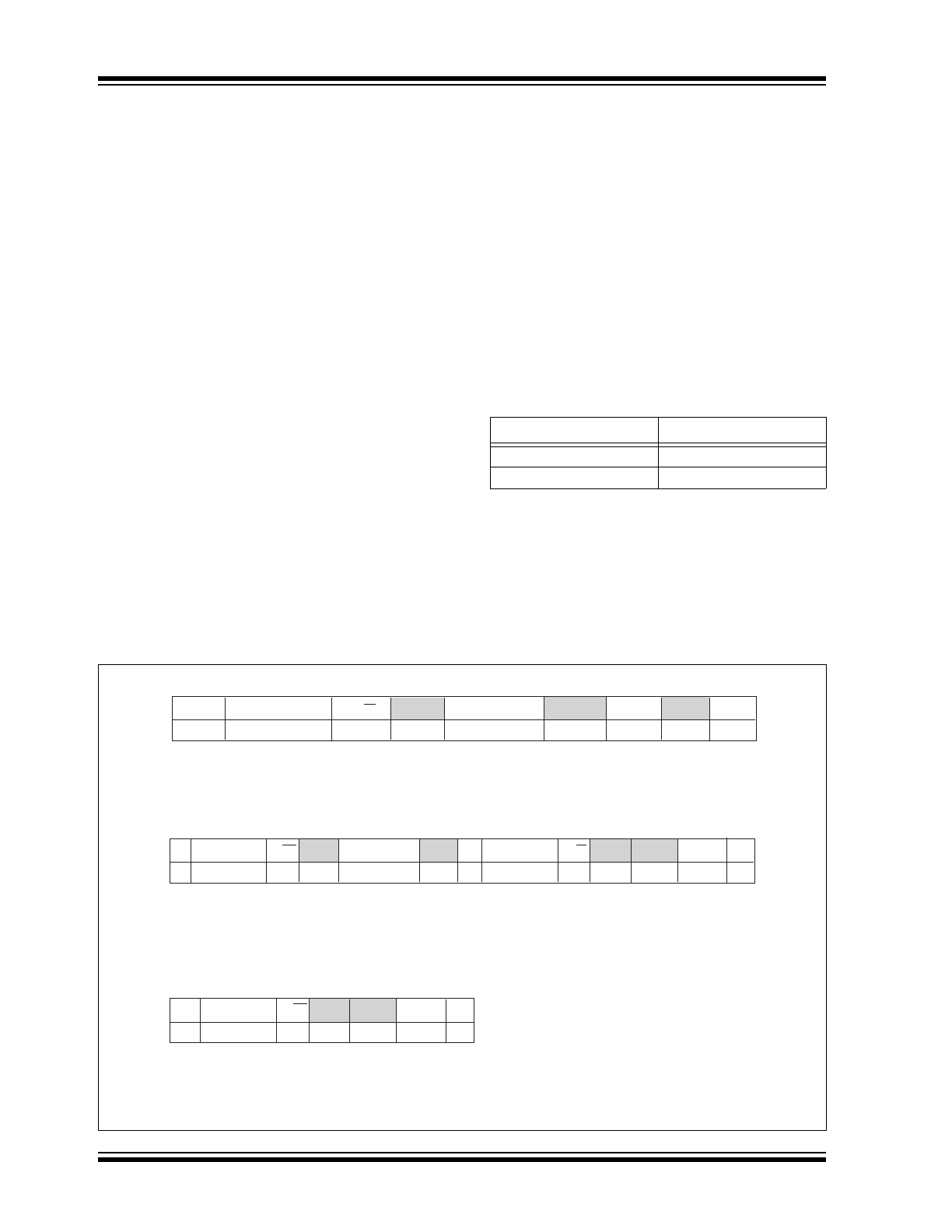
FIGURE 3-1:
SMBus PROTOCOLS
SHDN Bit
Operating Mode
0
Normal
1
Standby
S
Address
R/W
ACK
Command
ACK
Data
ACK
P
8-Bits
7-Bits
8-Bits
Slave Address
Command Byte: selects
which register you are
writing to.
Data Byte: data goes
into the register set
by the command byte.
Write 1-Byte Format
Read 1-Byte Format
S
Address
R/W
ACK
Command
ACK
S
Address
R/W ACK
Data
NACK
P
7-Bits
8-Bits
7-Bits
8-Bits
Slave Address
Command Byte: selects
which register you are
reading from.
Slave Address: repeated
due to change in data
flow direction.
Data Byte: reads from
the register set by the
command byte.
Receive 1-Byte Format
S
Address
R/W ACK
Data
NACK
P
7-Bits
1
1
0
0
8-Bits
Data Byte: reads data from
the register commanded by
the last Read Byte or Write
Byte transmission.
S = START Condition
P = STOP Condition
Shaded = Slave Transmission
2002-2012 Microchip Technology Inc.
DS21386C-page 7
TC1320
4.0
SERIAL PORT OPERATION
The Serial Clock input (SCL) and bi-directional data
port (SDA) form a 2-wire bi-directional serial port for
programming and interrogating the TC1320. The
following conventions are used in this bus architecture:
TABLE 4-1:
TC1320 SERIAL BUS
CONVENTIONS
All transfers take place under control of a host, usually
a CPU or microcontroller, acting as the Master, which
provides the clock signal for all transfers. The TC1320
always operates as a Slave. The serial protocol is illus-
trated in Figure 3-1. All data transfers have two phases;
all bytes are transferred MSB first. Accesses are initi-
ated by a START condition (START), followed by a
device address byte and one or more data bytes. The
device address byte includes a Read/Write selection
bit. Each access must be terminated by a STOP Con-
dition (STOP). A convention called Acknowledge
(ACK) confirms receipt of each byte. Note that SDA can
change only during periods when SCL is LOW (SDA
changes while SCL is HIGH is reserved for START and
STOP Conditions).
4.1
START Condition (START)
The TC1320 continuously monitors the SDA and SCL
lines for a START condition (a HIGH to LOW transition
of SDA while SCL is HIGH), and will not respond until
this condition is met.
4.2
Address Byte
Immediately following the START Condition, the host
must transmit the address byte to the TC1320. The
7-bit SMBus address for the TC1320 is 1001000. The
7-bit address transmitted in the serial bit stream must
match for the TC1320 to respond with an Acknowledge
(indicating the TC1320 is on the bus and ready to
accept data). The eighth bit in the Address Byte is a
Read/Write bit. This bit is a 1 for a read operation, or 0
for a write operation. During the first phase of any
transfer, this bit will be set = 0 to indicate that the
command byte is being written.
4.3
Acknowledge (ACK)
Acknowledge (ACK) provides a positive handshake
between the host and the TC1320. The host releases
SDA after transmitting eight bits, then generates a ninth
clock cycle to allow the TC1320 to pull the SDA line
LOW to Acknowledge that it successfully received the
previous eight bits of data or address.
4.4
Data Byte
After a successful ACK of the address byte, the host
must transmit the data byte to be written, or clock out
the data to be read. (See the appropriate timing dia-
grams.) ACK will be generated after a successful write
of a data byte into the TC1320.
4.5
STOP Condition (STOP)
Communications must be terminated by a STOP con-
dition (a LOW to HIGH transition of SDA while SCL is
HIGH). The STOP Condition must be communicated
by the transmitter to the TC1320. Refer to Figure 4-1,
Timing Diagrams for serial bus timing.
Term
Explanation
Transmitter The device sending data to the bus.
Receiver
The device receiving data from the bus.
Master
The device which controls the bus: initiating
transfers (START), generating the clock, and
terminating transfers (STOP).
Slave
The device addressed by the master.
START
A unique condition signaling the beginning of
a transfer indicated by SDA falling
(High - Low) while SCL is high.
STOP
A unique condition signaling the end of a
transfer indicated by SDA rising (Low - High)
while SCL is high.
ACK
A Receiver Acknowledges the receipt of each
byte with this unique condition. The Receiver
drives SDA low during SCL high of the ACK
clock pulse. The Master provides the clock
pulse for the ACK cycle.
Busy
Communication is not possible because the
bus is in use.
Not Busy
When the bus is IDLE, both SDA and SCL will
remain high.
Data Valid
The state of SDA must remain stable during
the High period of SCL in order for a data bit
to be considered valid. SDA only changes
state while SCL is low during normal data
transfers. (See START and STOP conditions.)
TC1320
DS21386C-page 8
2002-2012 Microchip Technology Inc.
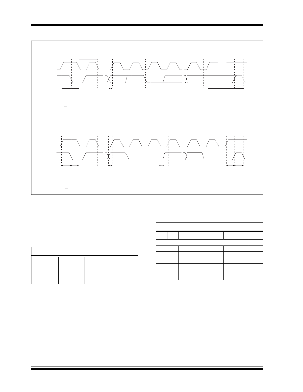
FIGURE 4-1:
TIMING DIAGRAMS
4.6
Register Set and Programmer’s
Model
TABLE 4-2:
TC1320 COMMAND SET
(SMBus READ_BYTE AND
WRITE_BYTE)
TABLE 4-3:
CONFIGURATION REGISTER
(CONFIG), 8-BIT, READ/WRITE
t
SU(START)
t
H(START)
t
SU-DATA
t
SU(STOP)
t
IDLE
A = START Condition
B = MSB of Address Clocked into Slave
C = LSB of Address Clocked into Slave
D = R/W Bit Clocked into Slave
A
SMBus Write Timing Diagram
SMBUS Read Timing Diagram
B
C
D
E
F
G
H
I
J
K
E = Slave Pulls SDA Line Low
F = Acknowledge Bit Clocked into Master
G = MSB of Data Clocked into Master
H = LSB of Data Clocked into Master
I
LOW
I
HIGH
I = Acknowledge Clock Pulse
J = STOP Condition
K = New START Condition
SCL
SDA
t
SU(START)
t
H(START)
t
SU-DATA
t
H-DATA
t
SU(STOP
) t
IDLE
A = START Condition
B = MSB of Address Clocked into Slave
C = LSB of Address Clocked into Slave
D = R/W Bit Clocked into Slave
E = Slave Pulls SDA Line Low
A
B
C
D
E
F
G
H
I
J
K
L
M
F = Acknowledge Bit Clocked into Master
G = MSB of Data Clocked into Slave
H = LSB of Data Clocked into Slave
I = Slave Pulls SDA Line Low
J = Acknowledge Clocked into Master
K = Acknowledge Clock Pulse
L = STOP Condition, Data Executed by Slave
M = New START Condition
ILOW IHIGH
SCL
SDA
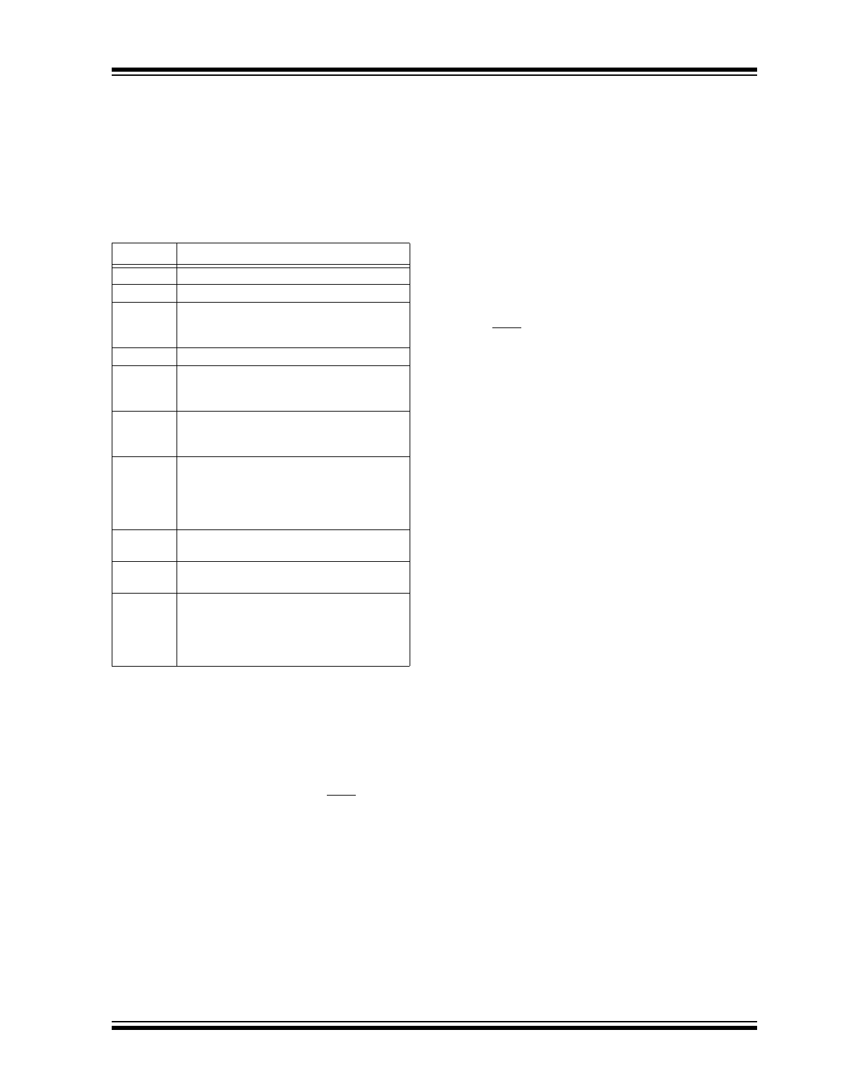
Command Byte Description
Command
Code
Function
RWD
00h
Read/Write Data (DATA)
RWCR
01h
Read/Write Configuration
(CONFIG)
Configuration Register (CONFIG)
D[7] D[6]
D[5]
D[4]
D[3]
D[2]
D[1]
D[0]
Reserved SHDN
Bit
POR
Function
Type
Operation
D[0]
0
Standby Switch
Read/
Write
1 = Standby
0 = Normal
D[7]-D[1]
0
Reserved;
Always returns
Zero when Read
N/A
N/A
2002-2012 Microchip Technology Inc.
DS21386C-page 9
TC1320
TABLE 4-4:
DATA REGISTER (DATA),
8-BIT, READ/WRITE
The DAC output voltage is a function of reference volt-
age and the binary value of the contents of the Data reg-
ister. The transfer function is given by the expression:
EQUATION 4-1:
4.7
Register Set Summary
The TC1320’s register set is summarized in Table 4-5
below. All registers are 8-bits wide.
TABLE 4-5:
TC1320 REGISTER SET
SUMMARY
Data Register (DATA)
D[7]
D[6]
D[5]
D[4]
D[3]
D[2]
D[1]
D[0]
MSB
X
X
X
X
X
X
LSB
V
OUT
V
REF
x
DATA
256
-----------------
=
Name
Description
POR State
Read
Write
Data
Data Register
0000 0000b
X
X
Config
CONFIG Register 0000 0000b
X
X
TC1320
DS21386C-page 10
2002-2012 Microchip Technology Inc.
5.0
PACKAGING INFORMATION
5.1
Package Marking Information
Package marking data not available at this time.
5.2
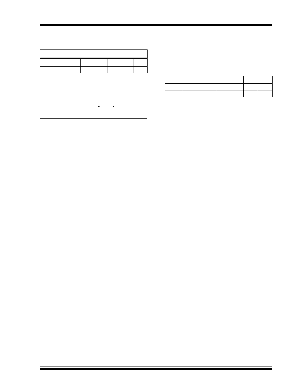
Taping Forms
Component Taping Orientation for 8-Pin MSOP Devices
Package
Carrier Width (W)
Pitch (P)
Part Per Full Reel
Reel Size
8-Pin MSOP
12 mm
8 mm
2500
13 in
Carrier Tape, Number of Components Per Reel and Reel Size
PIN 1
User Direction of Feed
Standard Reel Component Orientation
for TR Suffix Device
W
P
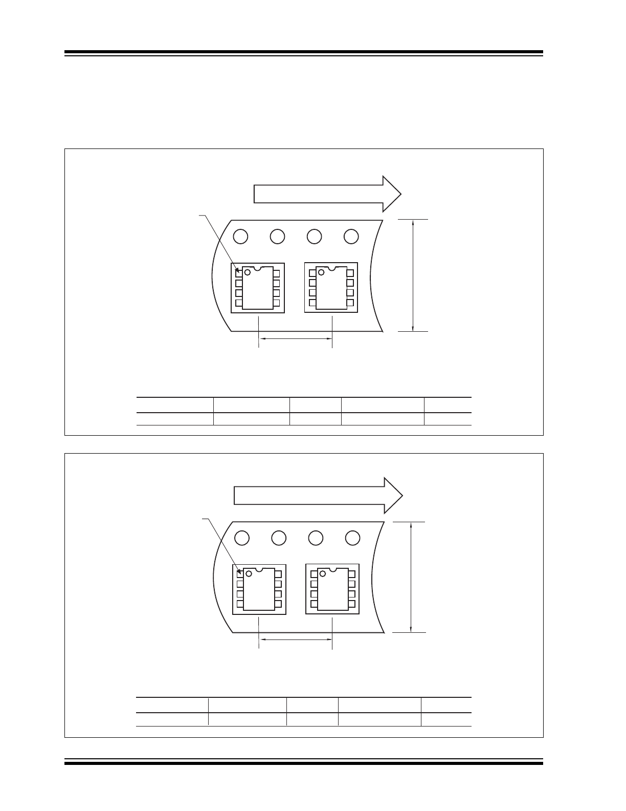
Component Taping Orientation for 8-Pin SOIC (Narrow) Devices
Package
Carrier Width (W)
Pitch (P)
Part Per Full Reel
Reel Size
8-Pin SOIC (N)
12 mm
8 mm
2500
13 in
Carrier Tape, Number of Components Per Reel and Reel Size
Standard Reel Component Orientation
for TR Suffix Device
PIN 1
User Direction of Feed
P
W