
2001-2012 Microchip Technology Inc.
DS21385D-page 1
Features
• LDO with Integrated Microcontroller Reset
Monitor Functionality
• Low Input Supply Current (80 µA, typical)
• Very Low Dropout Voltage
• 10 µsec (typ.) Wake-Up Time from SHDN
• 300 mA Output Current
• Standard or Custom Output and Detected
Voltages
• Power-Saving Shutdown Mode
• Bypass Input for Quiet Operation
• Separate Input for Detected Voltage
• 140 msec Minimum RESET Output Duration
• Space-Saving MSOP Package
• Specified Junction Temperature Range:
-40°C to +125°C
Applications
• Battery-Operated Systems
• Portable Computers
• Medical Instruments
• Pagers
• Cellular / GSM / PHS Phones
Related Literature
• AN765, “Using Microchip’s Micropower LDOs”,
DS00765.
• AN766, “Pin-Compatible CMOS Upgrades to
Bipolar LDOs”, DS00766.
• AN792, “A Method to Determine How Much
Power a SOT23 Can Dissipate in an Application”,
DS00792.
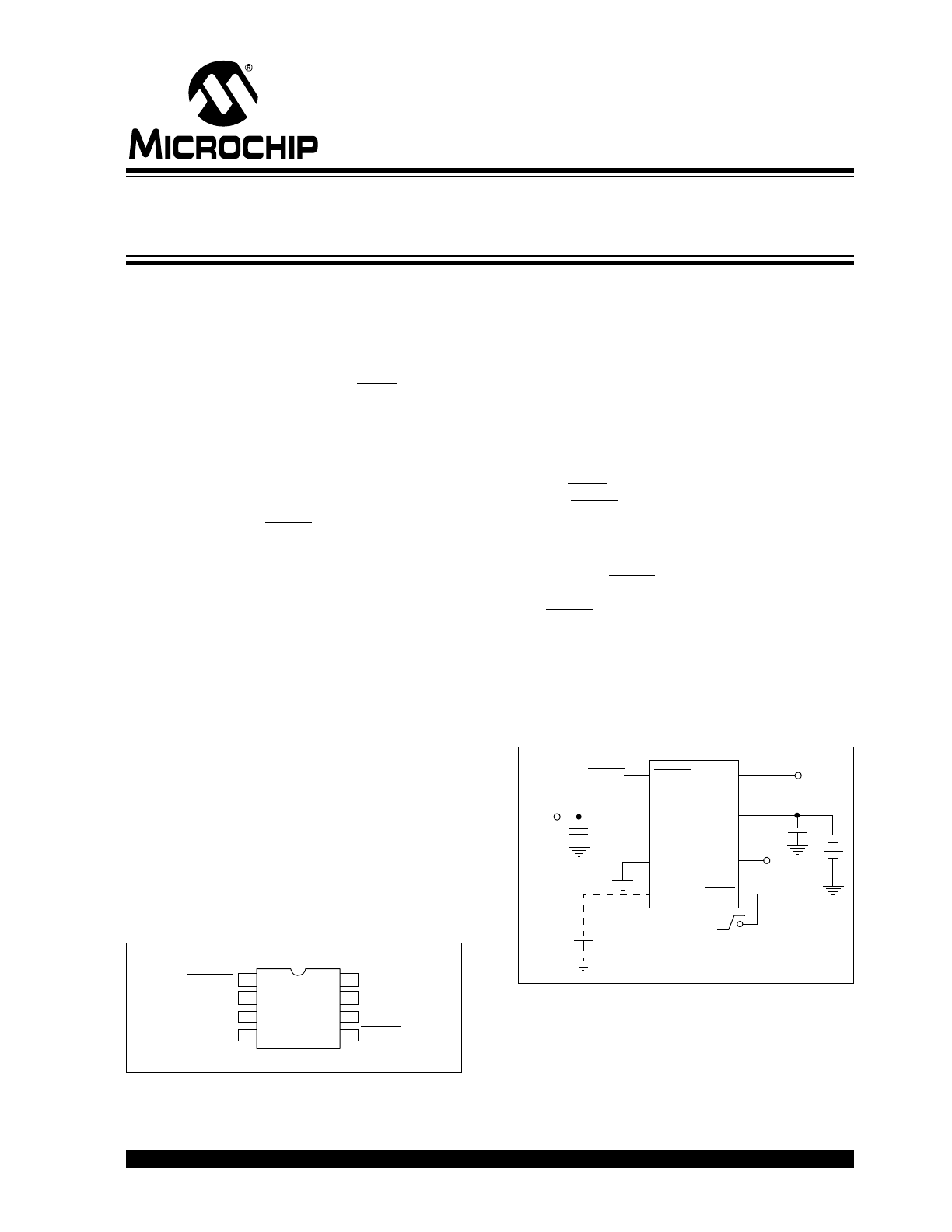
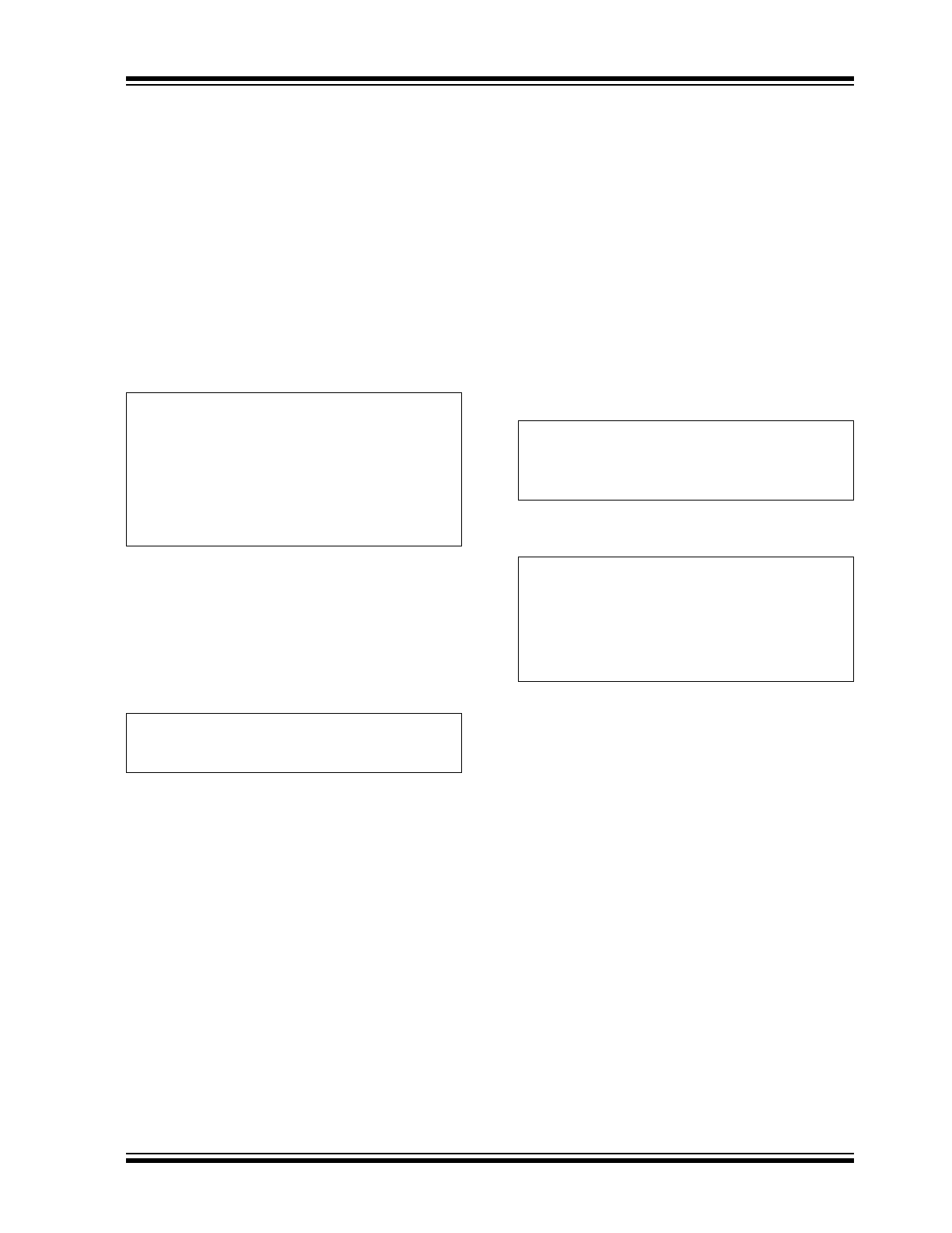
Package Type
General Description
The TC1300 combines a low dropout regulator and a
microcontroller reset monitor in an 8-Pin MSOP pack-
age. Total supply current is 80 µA (typical), 20 to 60
times lower than bipolar regulators.
The TC1300 has a precise output with a typical accu-
racy of ±0.5%. Other key features include low noise
operation, low dropout voltage and internal feed-
forward compensation for fast response to step
changes in load. The TC1300 has both over-tempera-
ture and over-current protection. When the shutdown
control (SHDN) is low, the regulator output voltage falls
to zero, RESET output remains valid and supply cur-
rent is reduced to 30 µA (typical). The TC1300 is rated
for 300 mA of output current and stable with a 1 µF out-
put capacitor.
An active-low RESET is asserted when the detected
voltage (V
DET
) falls below the reset voltage threshold.
The RESET output remains low for 300 msec (typical)
after V
DET
rises above reset threshold. The TC1300
also has a fast wake-up response time (10 µsec.,
typical) when released from shutdown.
Typical Application Circuit
1
2
3
4
V
IN
V
DET
5
6
7
8
NC
V
OUT
GND
Bypass
SHDN
RESET
TC1300VUA
MSOP
TC1300
1
2
3
4
5
6
7
8
V
OUT
C
BYPASS
470 pF
(Optional)
Shutdown Control
(from Power
Control Logic)
GND
Bypass
V
IN
SHDN
V
OUT
C
1
1 µF
RESET
RESET
V
DET
NC
C
2
1 µF
Battery
V
DET
+
TC1300
300 mA CMOS LDO with Shutdown, Bypass and
Independent Delayed Reset Function
TC1300
DS21385D-page 2
2001-2012 Microchip Technology Inc.
1.0
ELECTRICAL
CHARACTERISTICS
Absolute Maximum Ratings*
Input Voltage ....................................................................6.5V
Output Voltage ................................. (V
SS
- 0.3) to (V
IN
+ 0.3)
Power Dissipation ......................... Internally Limited (Note 6)
Operating Junction Temperature, T
J
....... – 40°C < T
J
< 150°C
Maximum Junction Temperature, Tj .............................. 150°C
Storage Temperature................................... – 65°C to +150°C
Maximum Voltage on Any Pin ............. (V
SS
-0.3) to (V
IN
+0.3)
*Notice: Stresses above those listed under “maximum rat-
ings” may cause permanent damage to the device. This is a
stress rating only and functional operation of the device at
those or any other conditions above those indicated in the
operational listings of this specification is not implied. Expo-
sure to maximum rating conditions for extended periods may
affect device reliability.
PIN DESCRIPTIONS
Pin
Description
RESET
RESET output remains low while V
DET
is
below the reset voltage threshold and for
300 msec after V
DET
rises above reset thesh-
old.
V
OUT
Regulated Voltage Output
GND
Ground Terminal
Bypass
Reference Bypass Input. Connecting an
optional 470 pF to this input further reduces
output noise.
SHDN
Shutdown Control Input. The regulator is fully
enabled when a logic high is applied to this
input. The regulator enters shutdown when a
logic low is applied to this input. During shut-
down, regulator output voltage falls to zero,
RESET output remains valid and supply cur-
rent is reduced to 30 µA (typ.).
NC
No connect
V
IN
Power Supply Input
V
DET
Detected Input Voltage. V
DET
and V
IN
can be
connected together.
ELECTRICAL CHARACTERISTICS
V
IN
= V
OUT
+ 1V, I
L
= 0.1 mA, C
L
= 3.3 µF, SHDN > V
IH
, T
A
= 25°C, unless otherwise noted. BOLDFACE type specifications apply
for junction temperature (Note 8) of -40°C to +125°C.
Parameters
Sym
Min
Typ
Max
Units
Conditions
Input Operating Voltage
V
IN
2.7
—
6.0
V
Note 7
Maximum Output Current
I
OUTMAX
300
—
—
mA
Output Voltage
V
OUT
—
V
R
- 2.5%
V
R
± 0.5%
—
—
V
R
+ 2.5%
V
Note 1
V
OUT
Temperature Coefficient
V
OUT
/
T
—
25
—
ppm/°C Note 2
Line Regulation
V
OUT
/
V
IN
—
0.02
0.35
%
(V
R
+ 1V) < V
IN
< 6V
Load Regulation
V
OUT
/V
OUT
—
0.5
2.0
%
I
L
= 0.1 mA to I
OUT
MAX,
Note 3
Note
1: V
R
is the regulator output voltage setting.
2:
3: Regulation is measured at a constant junction temperature using low duty cycle pulse testing. Load regulation is tested
over a load range from 0.1 mA to the maximum specified output current. Changes in output voltage due to heating
effects are covered by the thermal regulation specification.
4: Dropout voltage is defined as the input to output differential at which the output voltage drops 2% below its nominal value
measured at a 1V differential.
5: Thermal Regulation is defined as the change in output voltage at a time t after a change in power dissipation is applied,
excluding load or line regulation effects. Specifications are for a current pulse equal to I
LMAX
at V
IN
= 6V for t = 10 msec.
6: The maximum allowable power dissipation is a function of ambient temperature, the maximum allowable junction tem-
perature and the thermal resistance from junction-to-air (i.e. T
A
, T
J
,
JA
). Exceeding the maximum allowable power dissi-
pation causes the device to initiate thermal shutdown. Please see Section 4.0, “Thermal Considerations”, of this data
sheet for more details.
7: The minimum V
IN
has to meet two conditions: V
IN
2.7V and V
IN
(V
R
+ V
DROPOUT
).
8: The junction temperature of the device is approximated by soaking the device under test at an ambient temperature
equal to the desired junction temperature. The test time is small enough such that the rise in the junction temperature
over the ambient temperature is not significant.
TCV
OUT
V
OUTMAX
V
OUTMIN
–
10
6
V
OUT
T
--------------------------------------------------------------------------------------
=
2001-2012 Microchip Technology Inc.
DS21385D-page 3
TC1300
Dropout Voltage (Note 4)
V
IN –
V
OUT
—
1
70
210
30
130
390
mV
I
L
= 0.1 mA
I
L
= 100 mA
I
L
= 300 mA
Supply Current
I
SS1
—
80
160
µA
SHDN = V
IH
Shutdown Supply Current
I
SS2
—
30
60
µA
SHDN = 0V
Power Supply Rejection Ratio
PSRR
—
60
—
dB
f
1 kHz, C
BYPASS
= 1 nF
Output Short Circuit Current
I
OUTSC
—
800
1200
mA
V
OUT
= 0V
Thermal Regulation
V
OUT
/
P
D
— 0.04
—
%/W
Note 5
Output Noise
eN
—
900
—
nV/Hz
f < 1 kHz, C
OUT
= 1 µF,
R
LOAD
= 50
C
BYPASS
= 1 nF
Wake-Up Time
(from Shutdown Mode)
t
WK
—
10
20
µsec
C
IN
= 1 µF, V
IN
= 5V,
C
OUT
= 4.7 µF, I
L
= 30 mA,
See Figure 3-2
Settling Time
(from Shutdown Mode)
ts
—
50
—
µsec
C
IN
= 1 µF, V
IN
= 5V
C
OUT
= 4.7 µF
I
L
= 30 mA, See Figure 3-2
Thermal Shutdown Die
Temperature
T
SD
—
150
—
°C
Thermal Shutdown Hysteresis
T
HYS
—
10
—
°C
Thermal Resistance Junction to
Case
RthetaJA
—
200
—
°C/Watt EIA/JEDEC JESD51-751-7 4-
Layer Board
SHDN Input High Threshold
V
IH
45
—
—
%V
IN
V
IN
= 2.5V to 6.0V
SHDN Input Low Threshold
V
IL
—
—
15
%V
IN
V
IN
= 2.5V to 6.0V
ELECTRICAL CHARACTERISTICS (CONTINUED)
V
IN
= V
OUT
+ 1V, I
L
= 0.1 mA, C
L
= 3.3 µF, SHDN > V
IH
, T
A
= 25°C, unless otherwise noted. BOLDFACE type specifications apply
for junction temperature (Note 8) of -40°C to +125°C.
Parameters
Sym
Min
Typ
Max
Units
Conditions
Note
1: V
R
is the regulator output voltage setting.
2:
3: Regulation is measured at a constant junction temperature using low duty cycle pulse testing. Load regulation is tested
over a load range from 0.1 mA to the maximum specified output current. Changes in output voltage due to heating
effects are covered by the thermal regulation specification.
4: Dropout voltage is defined as the input to output differential at which the output voltage drops 2% below its nominal value
measured at a 1V differential.
5: Thermal Regulation is defined as the change in output voltage at a time t after a change in power dissipation is applied,
excluding load or line regulation effects. Specifications are for a current pulse equal to I
LMAX
at V
IN
= 6V for t = 10 msec.
6: The maximum allowable power dissipation is a function of ambient temperature, the maximum allowable junction tem-
perature and the thermal resistance from junction-to-air (i.e. T
A
, T
J
,
JA
). Exceeding the maximum allowable power dissi-
pation causes the device to initiate thermal shutdown. Please see Section 4.0, “Thermal Considerations”, of this data
sheet for more details.
7: The minimum V
IN
has to meet two conditions: V
IN
2.7V and V
IN
(V
R
+ V
DROPOUT
).
8: The junction temperature of the device is approximated by soaking the device under test at an ambient temperature
equal to the desired junction temperature. The test time is small enough such that the rise in the junction temperature
over the ambient temperature is not significant.
TCV
OUT
V
OUTMAX
V
OUTMIN
–
10
6
V
OUT
T
--------------------------------------------------------------------------------------
=
TC1300
DS21385D-page 4
2001-2012 Microchip Technology Inc.
RESET Output
Voltage Range
V
DET
1.0
1.2
—
—
6.0
6.0
V
T
A
= 0°C to +70°C
T
A
= – 40°C to +125°C
Reset Threshold
V
TH
2.59
2.63
2.66
V
TC1300R-XX, T
A
= +25°C
2.55
—
2.70
TC1300R-XX,
T
A
= – 40°C to +125°C
2.36
2.40
2.43
TC1300Y-XX, T
A
= +25°C
2.32
—
2.47
TC1300Y-XX,
T
A
= – 40°C to +125°C
Reset Threshold Tempco
V
TH
/
T
—
30
—
ppm/°C
V
DET
to Reset Delay
t
RPD
—
160
—
µsec
V
DET
= V
TH
to (V
TH
– 100 mV)
Reset Active Timeout Period
t
RPU
140
300
560
msec
RESET Output Voltage Low
V
OL
—
—
0.3
V
V
DET
= V
TH
min,
I
SINK
= 1.2 mA
RESET Output Voltage High
V
OH
0.8 V
DET
—
—
V
V
DET
> V
TH
max,
I
SOURCE
= 500 µA
ELECTRICAL CHARACTERISTICS (CONTINUED)
V
IN
= V
OUT
+ 1V, I
L
= 0.1 mA, C
L
= 3.3 µF, SHDN > V
IH
, T
A
= 25°C, unless otherwise noted. BOLDFACE type specifications apply
for junction temperature (Note 8) of -40°C to +125°C.
Parameters
Sym
Min
Typ
Max
Units
Conditions
Note
1: V
R
is the regulator output voltage setting.
2:
3: Regulation is measured at a constant junction temperature using low duty cycle pulse testing. Load regulation is tested
over a load range from 0.1 mA to the maximum specified output current. Changes in output voltage due to heating
effects are covered by the thermal regulation specification.
4: Dropout voltage is defined as the input to output differential at which the output voltage drops 2% below its nominal value
measured at a 1V differential.
5: Thermal Regulation is defined as the change in output voltage at a time t after a change in power dissipation is applied,
excluding load or line regulation effects. Specifications are for a current pulse equal to I
LMAX
at V
IN
= 6V for t = 10 msec.
6: The maximum allowable power dissipation is a function of ambient temperature, the maximum allowable junction tem-
perature and the thermal resistance from junction-to-air (i.e. T
A
, T
J
,
JA
). Exceeding the maximum allowable power dissi-
pation causes the device to initiate thermal shutdown. Please see Section 4.0, “Thermal Considerations”, of this data
sheet for more details.
7: The minimum V
IN
has to meet two conditions: V
IN
2.7V and V
IN
(V
R
+ V
DROPOUT
).
8: The junction temperature of the device is approximated by soaking the device under test at an ambient temperature
equal to the desired junction temperature. The test time is small enough such that the rise in the junction temperature
over the ambient temperature is not significant.
TCV
OUT
V
OUTMAX
V
OUTMIN
–
10
6
V
OUT
T
--------------------------------------------------------------------------------------
=
2001-2012 Microchip Technology Inc.
DS21385D-page 5
TC1300
2.0
TYPICAL CHARACTERISTICS
Junction temperature (T
J
) is approximated by soaking the device under test at an ambient temperature equal to the
desired Junction temperature. The test time is small enough such that the rise in the Junction temperature over the
Ambient temperature is not significant.
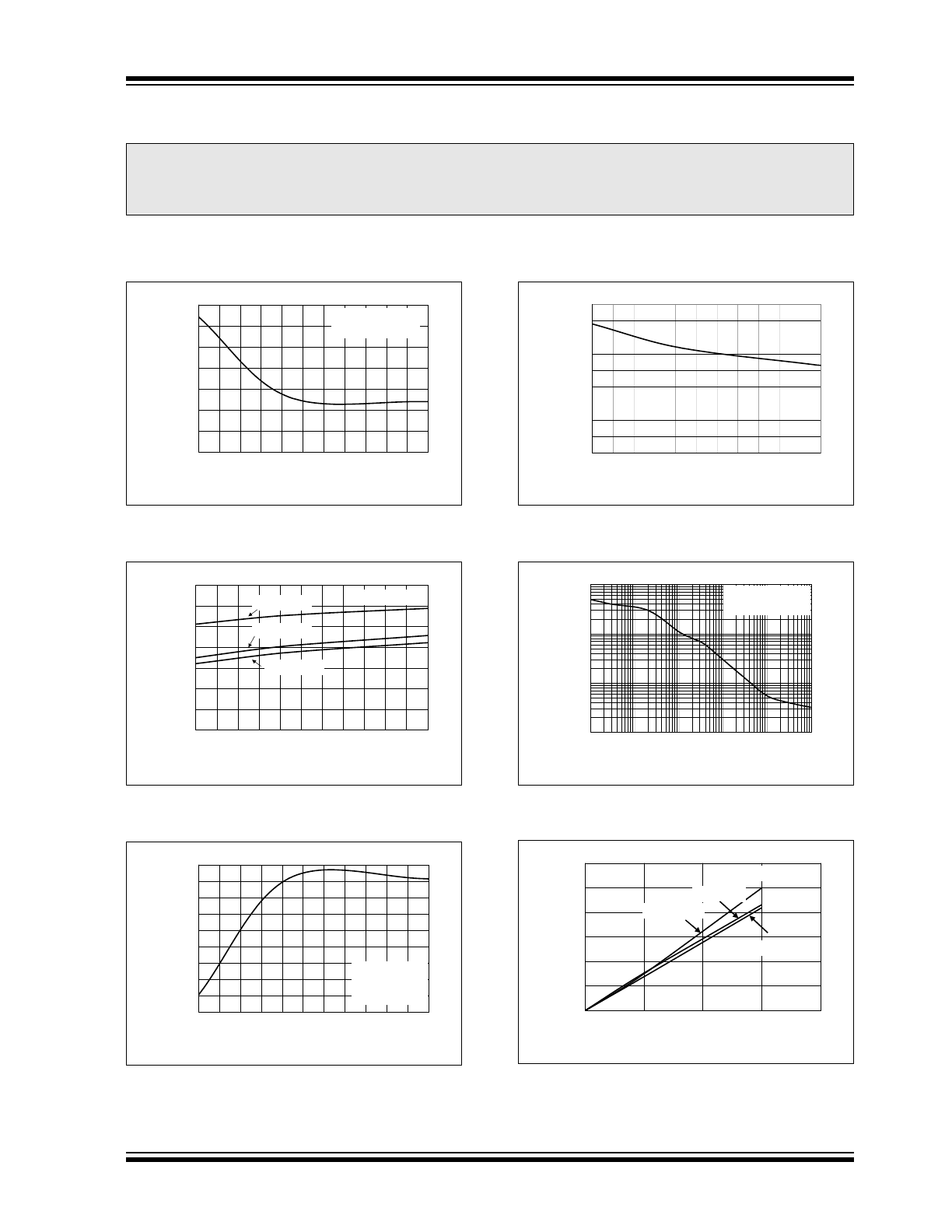
FIGURE 2-1:
Line Regulation vs.
Temperature.
FIGURE 2-2:
Supply Current vs.
Temperature.
FIGURE 2-3:
Normalized V
OUT
vs.
Temperature.
FIGURE 2-4:
Reset Active Time-out
Period vs. Temperature.
FIGURE 2-5:
Output Noise vs. Frequency.
FIGURE 2-6:
Dropout Voltage vs. Load
Current (2.5V).
Note:
The graphs and tables provided following this note are a statistical summary based on a limited number of
samples and are provided for informational purposes only. The performance characteristics listed herein
are not tested or guaranteed. In some graphs or tables, the data presented may be outside the specified
operating range (e.g., outside specified power supply range) and therefore outside the warranted range.
0.000
0.005
0.010
0.015
0.020
0.025
0.030
0.035
-40 -25 -10
5
20
35
50
65
80
95 110 125
Junction Temperature (°C)
Li
ne Regul
at
ion (
%
)
V
OUT
= 3.0V
V
IN
= 3.5V to 6.0V
0.00
0.02
0.04
0.06
0.08
0.10
0.12
0.14
-40 -25 -10
5
20 35 50 65 80 95 110 125
Junction Temperature (°C)
Suppl
y Cur
re
nt
(
m
A)
V
OUT
= 2.5V
V
OUT
= 5.0V
V
OUT
= 3.0V
V
IN
= V
OUT
+ 1V
2.491
2.492
2.493
2.494
2.495
2.496
2.497
2.498
2.499
2.500
-40 -25 -10
5
20
35
50
65
80
95 110 125
Junction Temperature (°C)
O
u
tput
Vol
tage (
V
)
V
IN
= V
OUT
+ 1V
I
OUT
= 100 µA
V
OUT
= 2.5V
0
50
100
150
200
250
300
350
400
450
-40 -25 -10
5
20
35
50
65
80
95 110 125
Junction Temperature (°C)
Reset Active Time-out Period
(ms)
0.01
0.10
1.00
10.00
0.01
0.10
1.00
10.00
100.00
1000.00
Frequency (kHz)
Ou
tp
u
t N
o
is
e
(µ
V
/lH
z
)
R
LOAD
= 50 Ohms
C
OUT
= 1 µF
1
1000
100
10
0.00
0.05
0.10
0.15
0.20
0.25
0.30
0
100
200
300
400
Load Current (mA)
Dr
opout
Vol
tage (
V
)
T
J
= +125°C
T
J
= -40°C
T
J
= +25°C
V
OUT
= 2.5V
TC1300
DS21385D-page 6
2001-2012 Microchip Technology Inc.
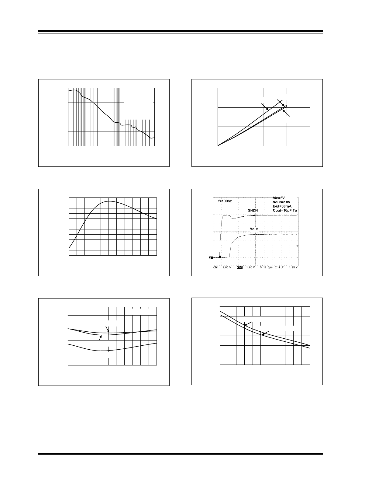
2.0 TYPICAL CHARACTERISTICS
(CON’T)
Junction temperature (T
J
) is approximated by soaking the device under test at an ambient temperature equal to the
desired Junction temperature. The test time is small enough such that the rise in the Junction temperature over the
Ambient temperature is not significant.
FIGURE 2-7:
Power Supply Rejection
Ratio vs. Frequency.
FIGURE 2-8:
Reset Voltage Threshold vs.
Junction Temperature.
FIGURE 2-9:
Load Regulation vs.
Temperature.
FIGURE 2-10:
Dropout Voltage vs. Load
Current (5.0V).
FIGURE 2-11:
Wake-Up Response Time.
FIGURE 2-12:
V
DET
to Reset Delay vs.
Temperature.
0
15
30
45
60
10
100
1000
10000
100000 100000
Frequency (Hz)
Power Supply Ripple Rejection
(dB)
V
IN
= 3.8V
V
OUT
= 2.8V
I
OUT
= 50 mA
C
OUT
= 10 μF
C
OUTesr
= 0.25 :
C
BYPASS
= 0 μF
1k
10k
100k
1M
2.6275
2.6280
2.6285
2.6290
2.6295
2.6300
2.6305
2.6310
2.6315
2.6320
2.6325
2.6330
-40 -25 -10
5
20
35
50
65
80
95 110 125
Junction Temperature (°C)
R
eset
Vol
tage Thr
eshol
d (
V
)
0.20
0.30
0.40
0.50
0.60
0.70
0.80
0.90
-40 -25 -10
5
20
35
50
65
80
95 110 125
Junction Temperature (°C)
Load Regulation (1 mA to 300
mA) %
V
IN
= V
OUT
+ 1V
V
OUT
= 3.0V
V
OUT
= 2.5V
V
OUT
= 5.0V
0
0.05
0.1
0.15
0.2
0.25
0.3
0
100
200
300
400
Load Current (mA)
Dr
opout
Vol
tage (
V
)
T
J
= +125°C
T
J
= -40°C
T
J
= +25°C
V
OUT
= 5.0V
0
50
100
150
200
250
300
-40 -25 -10
5
20
35
50
65
80
95 110 125
Junction Temperature (°C)
V
DET
to RESET Delay Time (µS)
10 mV Overdrive
100 mV Overdrive
2001-2012 Microchip Technology Inc.
DS21385D-page 7
TC1300
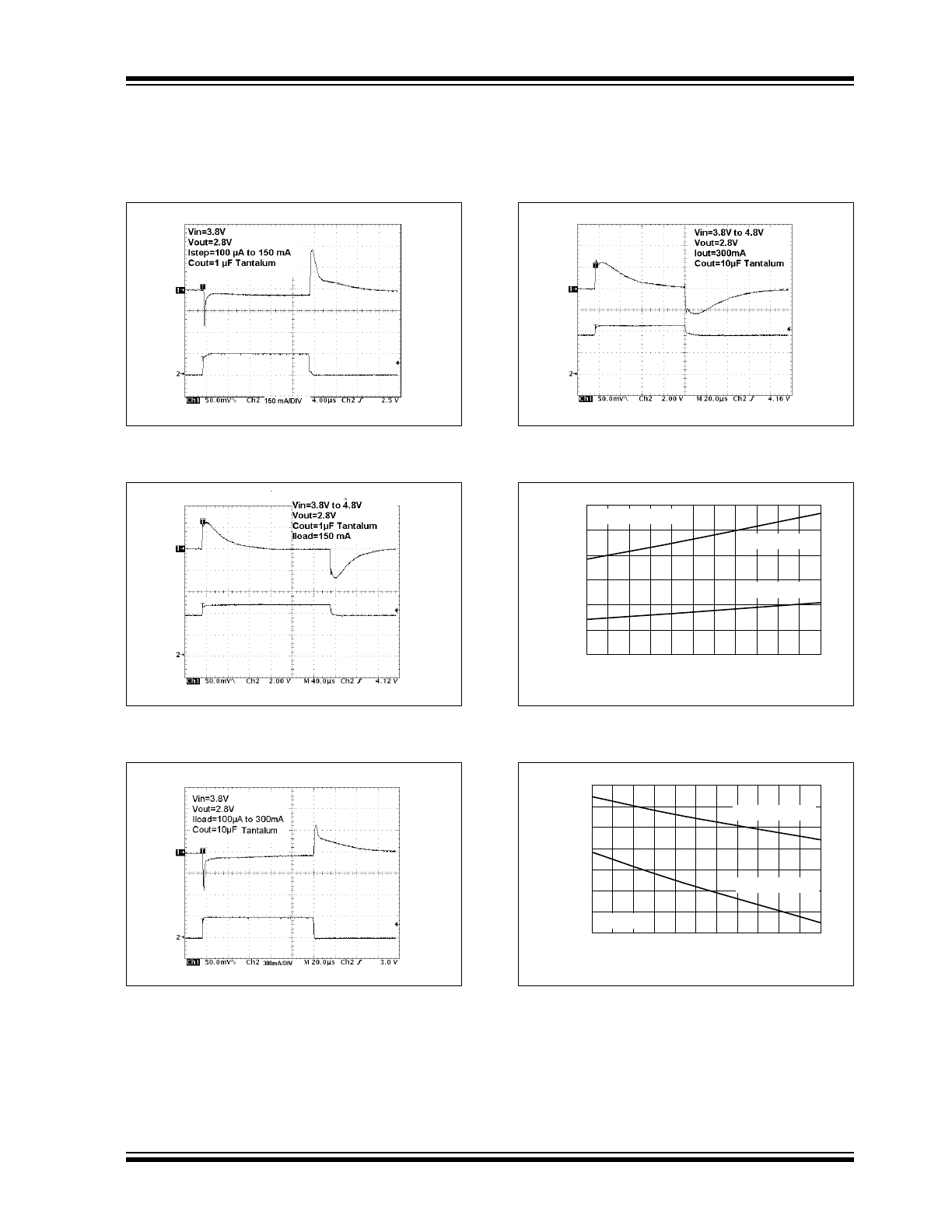
2.0 TYPICAL CHARACTERISTICS
(CON’T)
Junction temperature (T
J
) is approximated by soaking the device under test at an ambient temperature equal to the
desired Junction temperature. The test time is small enough such that the rise in the Junction temperature over the
Ambient temperature is not significant.
FIGURE 2-13:
Load Transient Response
1 µF Output Capacitor.
FIGURE 2-14:
Line Transient Response
1 µF Output Capacitor.
FIGURE 2-15:
Load Transient Response
10 µF Output Capacitor.
FIGURE 2-16:
Line Transient Response
10 µF Output Capacitor.
FIGURE 2-17:
RESET Output Voltage Low
vs. Junction Temperature.
FIGURE 2-18:
RESET Output Voltage High
vs. Junction Temperature.
0.00
0.05
0.10
0.15
0.20
0.25
0.30
-40 -25 -10
5
20
35
50
65
80
95 110 125
Junction Temperature (°C)
RESET V
OL
(V
)
V
DET
= V
TH
- 20 mV
I
SINK
= 1.2 mA
I
SINK
= 3.2 mA
3.890
3.900
3.910
3.920
3.930
3.940
3.950
3.960
-40 -25 -10
5
20
35
50
65
80
95 110 125
Junction Temperature (°C)
RESET VO
H (
V
)
V
DET
= 4.0V
I
SOURCE
= 500 µA
I
SOURCE
= 800 µA
TC1300
DS21385D-page 8
2001-2012 Microchip Technology Inc.
3.0
DETAILED DESCRIPTION
The TC1300 is a combination of a fixed output, low
dropout regulator and a microcontroller
monitor/RESET. Unlike bipolar regulators, the TC1300
supply current does not increase with load current. In
addition, V
OUT
remains stable and within regulation
over the entire specified operating load range (0 mA to
300 mA) and operating input voltage range (2.7V to
6.0V).
Figure 3-1 shows a typical application circuit. The reg-
ulator is enabled any time the shutdown input (SHDN)
is above V
IH
. The regulator is shutdown (disabled)
when SHDN is at or below V
IL
. SHDN may be con-
trolled by a CMOS logic gate or an I/O port of a micro-
controller. If the SHDN input is not required, it should be
connected directly to the input supply. While in shut-
down, supply current decreases to 30 µA (typical),
V
OUT
falls to zero and RESET remains valid.
3.1
RESET
Output
The RESET output is driven active-low within 160 µsec
of V
DET
falling through the reset voltage threshold.
RESET is maintained active for a minimum of
140 msec after V
DET
rises above the reset threshold.
The TC1300 has an active-low RESET output. The out-
put of the TC1300 is valid down to V
DET
= 1V and is
optimized to reject fast transient glitches on the V
DET
line.
FIGURE 3-1:
Typical Application Circuit.
3.2
Output Capacitor
A 1 µF (min) capacitor from V
OUT
to ground is required.
A 1 µF capacitor should also be connected from V
IN
to
GND if there is more than 10 inches of wire between
the regulator and the AC filter capacitor, or if a battery
is used as the power source. As with all low dropout
regulators, a minimum output capacitance is required
to stabilize the output voltage. For the TC1300, a mini-
mum of 1 µF of output capacitance is enough to stabi-
lize the device over the entire operating load and line
range. The selected output capacitor plays an impor-
tant role is compensating the LDO regulator. For the
TC1300, the selected output capacitor equivalent
series resistance (ESR) range is 0.1 ohms to 5 ohms
when using 1 µF of output capacitance, and 0.01 ohms
to 5 ohms when using 10 µF of output capacitance.
Because of the ESR requirement, tantalum and alumi-
num electrolytic capacitors are recommended. Alumi-
num electrolytic capacitors are not recommended for
operation at temperatures below -25°C. When operat-
ing from sources other than batteries, rejection and
transient responses can be improved by increasing the
value of the input and output capacitors and employing
passive filtering techniques.
3.3
Bypass Input (Optional)
An optional 470 pF capacitor connected from the
Bypass input to ground reduces noise present on the
internal reference, which in turn significantly reduces
output noise and improves PSRR performance. This
input may be left unconnected. Larger capacitor values
may be used, but results in a longer time period to rated
output voltage when power is initially applied.
3.4
Turn On Response
The turn-on response is defined as two separate
response categories, Wake-Up Time (t
WK
) and Settling
Time (t
S
).
The TC1300 has a fast Wake-Up Time (10 µsec typi-
cal) when released from shutdown. See Figure 3-2 for
the Wake-Up Time designated as t
WK
. The Wake-Up
Time is defined as the time it takes for the output to rise
to 2% of the V
OUT
value after being released from
shutdown.
The total turn-on response is defined as the Settling
Time (t
S
) (see Figure 3-2). Settling Time (inclusive with
t
WK
) is defined as the condition when the output is
within 2% of its fully enabled value (50 µsec typical)
when released from shutdown. The settling time of the
output voltage is dependent on load conditions and
output capacitance on V
OUT
(RC response).
FIGURE 3-2:
Wake-Up Response Time.
TC1300
1
2
3
4
5
6
7
8
V
OUT
C
BYPASS
470 pF
(Optional)
Shutdown Control
(from Power
Control Logic)
GND
Bypass
V
IN
SHDN
V
OUT
C
1
1 µF
RESET
V
DET
NC
C
2
1 µF
Battery
V
DET
+
RESET
Microcontroller
V
IH
t
S
t
WK
V
OUT
98%
2%
V
IL
SHDN
2001-2012 Microchip Technology Inc.
DS21385D-page 9
TC1300
4.0
THERMAL CONSIDERATIONS
4.1
Thermal Shutdown
Integrated thermal protection circuitry shuts the regula-
tor off when the die temperature exceeds 150°C. The
regulator remains off until the die temperature drops to
approximately 140°C.
4.2
Power Dissipation
The amount of power the regulator dissipates is primar-
ily a function of input and output voltage, and output
current. The following equation is used to calculate
worst case actual power dissipation:
EQUATION
The maximum allowable power dissipation, P
DMAX
, is a
function of the maximum ambient temperature (T
AMAX
),
the maximum recommended die temperature (125°C)
and the thermal resistance from junction-to-air (
JA
).
The MSOP-8 package has a
JA
of approximately
200°C/Watt when mounted on a FR4 dielectric copper
clad PC board.
EQUATION
The worst case actual power dissipation equation can
be used in conjunction with the LDO maximum allow-
able power dissipation equation to ensure regulator
thermal operation is within limits. For example:
Find:
EQUATION:
ACTUAL POWER
DISSIPATION
EQUATION:
MAXIMUM ALLOWABLE
POWER DISSIPATION
In this example, the TC1300 dissipates a maximum of
only 220 mW; below the allowable limit of 350 mW. In a
similar manner, the maximum actual power dissipation
equation and the maximum allowable power dissipa-
tion equation can be used to calculate maximum cur-
rent and/or input voltage limits. For example, the
maximum allowable V
IN
is found by substituting the
maximum allowable power dissipation of 350 mW into
the actual power dissipation equation, from which
V
INMAX
= 4.97V.
4.3
Layout Considerations
The primary path of heat conduction out of the package
is via the package leads. Therefore, layouts having a
ground plane, wide traces at the pads and wide power
supply bus lines combine to lower
JA
and, therefore,
increase the maximum allowable power dissipation
limit.
P
D
V
IN MAX
V
OUTMIN
–
I
LOA DMAX
Where:
P
D
= worst case actual power dissipation
V
INMAX
= maximum voltage on V
IN
V
OUTMIN
= minimum regulator output voltage
I
LOADMAX
= maximum output (load) current
P
DMAX
T
JMAX
T
AMAX
–
JA
--------------------------------------------
=
Given:
V
INMAX
=
4.1V
V
OUTMIN
=
3.0V -2.5%
I
LOADMAX
=
200 mA
T
JMAX
=
125°C
T
AMAX
=
55°C
JA
=
200°C/W
P
D
V
IN MAX
V
OUTMIN
–
I
LOA DMAX
4.1
3.0
.975
–
=
200
10
3
–
220 mW
=
P
DMAX
T
JMAX
T
AMAX
–
JA
--------------------------------------------
=
125
55
–
200
-------------------------
=
350 mW
=
TC1300
DS21385D-page 10
2001-2012 Microchip Technology Inc.
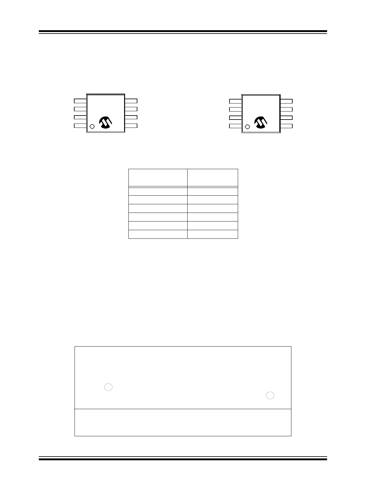
5.0
PACKAGING INFORMATION
5.1
Package Marking Information
Part Number
Marking Code
(XXXXXX)
TC1300R - 2.5VUA
1300RA
TC1300Y - 2.7VUA
1300YF
TC1300R - 2.8VUA
1300RB
TC1300R - 2.85VUA
1300RC
TC1300R - 3.0VUA
1300RD
TC1300R - 3.3VUA
1300RE
8-Lead MSOP
Example:
XXXXXX
YWWNNN
1300RA
YWWNNN
Legend: XX...X
Customer-specific information
Y
Year code (last digit of calendar year)
YY
Year code (last 2 digits of calendar year)
WW
Week code (week of January 1 is week ‘01’)
NNN
Alphanumeric traceability code
Pb-free JEDEC designator for Matte Tin (Sn)
*
This package is Pb-free. The Pb-free JEDEC designator ( )
can be found on the outer packaging for this package.
Note:
In the event the full Microchip part number cannot be marked on one line, it will
be carried over to the next line, thus limiting the number of available
characters for customer-specific information.
3
e
3
e