
2002-2012 Microchip Technology Inc.
DS21380C-page 1
TC1269
Features
• Very Low Ground Current for Longer Battery Life
• Very Low Dropout Voltage
• 300mA Output Circuit
• High Output Voltage Accuracy
• Standard or Custom Output Voltages
• Power Saving Shutdown Mode
• Bypass Input for Ultra Quiet Operation
• Over Current and Over Temperature Protection
• Space-Saving MSOP Package
Applications
• Battery Operated Systems
• Portable Computers
• Medical Instruments
• Instrumentation
• Cellular/GSM/PHS Phones
• Linear Post-Regulator for SMPS
• Pagers
• Digital Cameras
Device Selection Table
*Other output voltages are available. Please contact Microchip
Technology Inc. for details.
Package Type
General Description
The TC1269 is a fixed output, high accuracy (typically
±0.5%) CMOS upgrade for older (bipolar) low dropout
regulators. Total supply current is typically 50
A at full
load (20 to 60 times lower than in bipolar regulators).
TC1269 key features include ultra low noise operation
(plus optional Bypass input); very low dropout voltage
(typically 240mV at full load), and fast response to step
changes in load. Supply current is reduced to 0.05
A
(typical) and V
OUT
falls to zero when the shutdown
input is low.
The TC1269 incorporates both over temperature and
over current protection. The TC1269 is stable with an
output capacitor of only 1
F and has a maximum
output current of 300mA.
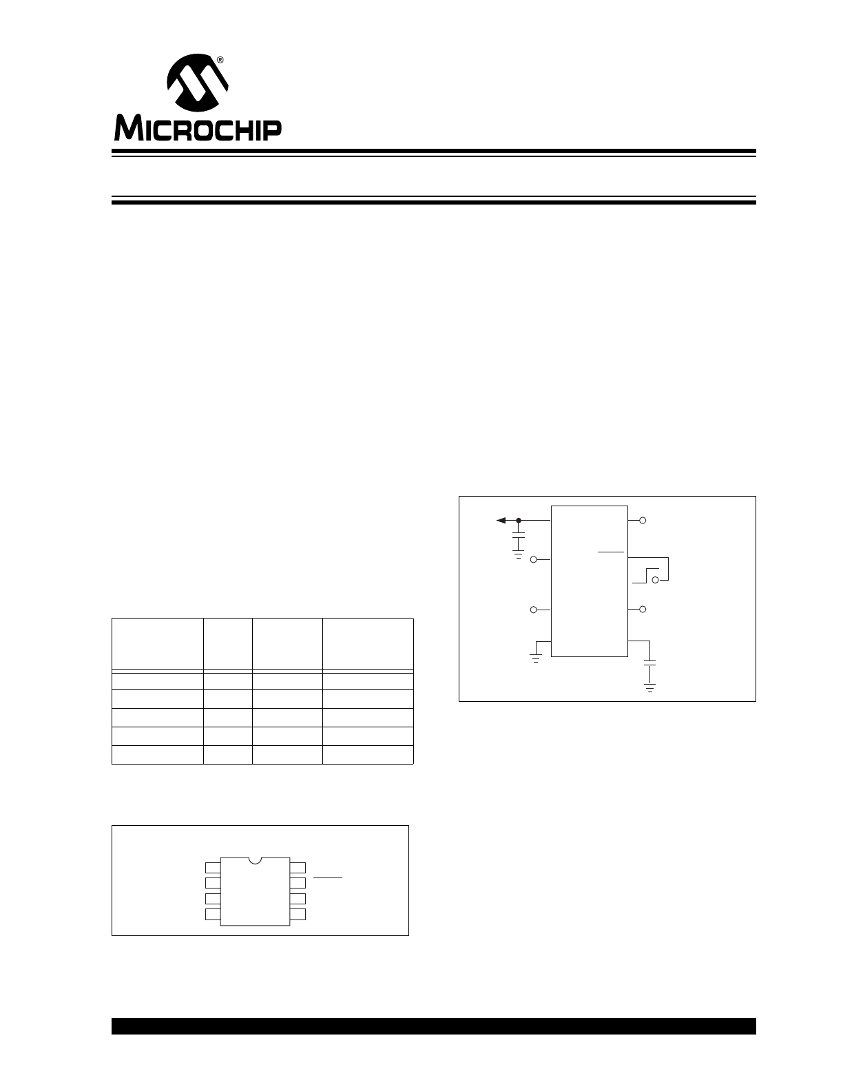
Typical Application
Part Number
Output*
Voltage
(V)
Package
Junction
Temp. Range
TC1269-2.5VUA
2.5
8-Pin MSOP -40°C to +125°C
TC1269-2.8VUA
2.8
8-Pin MSOP -40°C to +125°C
TC1269-3.0VUA
3.0
8-Pin MSOP -40°C to +125°C
TC1269-3.3VUA
3.3
8-Pin MSOP -40°C to +125°C
TC1269-5.0VUA
5.0
8-Pin MSOP -40°C to +125°C
8-Pin MSOP
V
IN
SHDN
Bypass
V
OUT
NC
NC
GND
NC
TC1269
1
2
3
4
5
6
7
8
TC1269
1
2
3
4
6
7
8
V
OUT
V
OUT
C
BYPASS
470pF
(Optional)
Shutdown Control
(from Power
Control Logic)
C1
1
µF
NC
NC
GND
Bypass
V
IN
V
IN
NC
SHDN
+
300mA CMOS LDO with Shutdown and V
REF
Bypass
TC1269
DS21380C-page 2
2002-2012 Microchip Technology Inc.
1.0
ELECTRICAL
CHARACTERISTICS
Absolute Maximum Ratings*
Input Voltage .........................................................6.5V
Output Voltage.................... (V
SS
– 0.3) to (V
IN
+ 0.3V)
Maximum Voltage on Any Pin ........V
IN
+0.3V to -0.3V
Power Dissipation................Internally Limited (Note 6)
Operating Temperature ............... -40°C < T
J
< +125°C
Storage Temperature..........................-65°C to +150°C
*Stresses above those listed under "Absolute Maximum
Ratings" may cause permanent damage to the device. These
are stress ratings only and functional operation of the device
at these or any other conditions above those indicated in the
operation sections of the specifications is not implied.
Exposure to Absolute Maximum Rating conditions for
extended periods may affect device reliability.
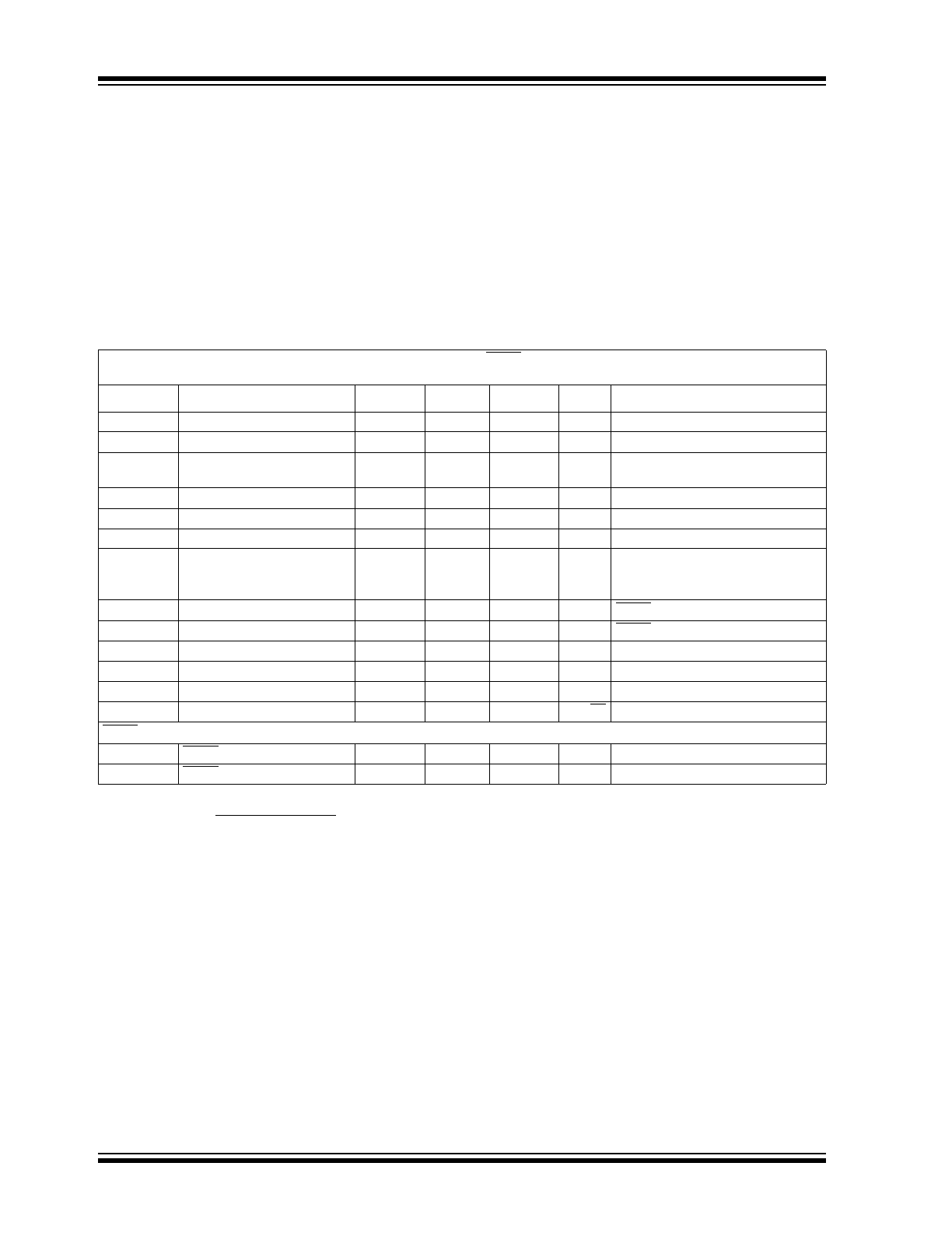
TC1269 ELECTRICAL SPECIFICATIONS
Electrical Characteristics: V
IN
= V
OUT
+ 1V, I
L
= 0.1
A, C
L
= 3.3
F, SHDN > V
IH
, T
A
= 25°C, unless otherwise noted. Boldface
type specifications apply for junction temperatures of -40°C to +125°C.
Symbol
Parameter
Min
Typ
Max
Units
Test Conditions
V
IN
Input Operating Voltage
—
—
6.0
V
I
OUT
MAX
Maximum Output Current
300
—
—
mA
V
OUT
Output Voltage
—
V
R
– 2.5%
V
R
±0.5%
—
—
V
R
+ 2.5%
V
Note 1
V
OUT
/
T
V
OUT
Temperature Coefficient
—
40
—
ppm/°C Note 2
V
OUT
/
V
IN
Line Regulation
—
0.05
0.35
%
(V
R
+ 1V)
V
IN
6V
V
OUT
/V
OUT
Load Regulation
—
0.5
2.0
%
I
L
= 0.1mA to I
OUT
MAX
V
IN
-V
OUT
Dropout Voltage
—
—
—
20
80
240
30
160
480
mV
I
L
= 0.1mA
I
L
= 100mA
I
L
= 300mA (Note 4)
I
SS1
Supply Current
—
50
90
A
SHDN = V
IH
I
SS2
Shutdown Supply Current
—
0.05
0.5
A
SHDN = 0V
PSRR
Power Supply Rejection Ratio
—
50
—
dB
F
RE
120Hz
I
OUTSC
Output Short Circuit Current
—
550
650
mA
V
OUT
= 0V
V
OUT
/
P
D
Thermal Regulation
—
0.04
—
V/W
Note 5
eN
Output Noise
—
260
—
nV/
Hz F = 1kHz, C
OUT
= 1
F, R
LOAD
= 50
SHDN Input
V
IH
SHDN Input High Threshold
45
—
—
%V
IN
V
IL
SHDN Input Low Threshold
—
—
15
%V
IN
Note 1:
V
R
is the regulator output voltage setting.
2:
3:
Regulation is measured at a constant junction temperature using low duty cycle pulse testing. Load regulation is tested over a load range from
0.1mA to the maximum specified output current. Changes in output voltage due to heating effects are covered by the thermal regulation specifica-
tion.
4:
Dropout voltage is defined as the input to output differential at which the output voltage drops 2% below its nominal value measured at a 1V differen-
tial.
5:
Thermal Regulation is defined as the change in output voltage at a time T after a change in power dissipation is applied, excluding load or
line regulation effects. Specifications are for a current pulse equal to I
L
MAX
at V
IN
= 6V for T = 10 msec.
6:
The maximum allowable power dissipation is a function of ambient temperature, the maximum allowable junction temperature and the
thermal resistance from junction-to-air (i.e., T
A
, T
J
,
JA
). Exceeding the maximum allowable power dissipation causes the device to initiate
thermal shutdown. Please see Section 4.0 Thermal Considerations for more details.
T
C
V
OUT
= (V
OUT
MAX
– V
OUT
MIN
) x 10
6
V
OUT
x
T
2002-2012 Microchip Technology Inc.
DS21380C-page 3
TC1269
2.0
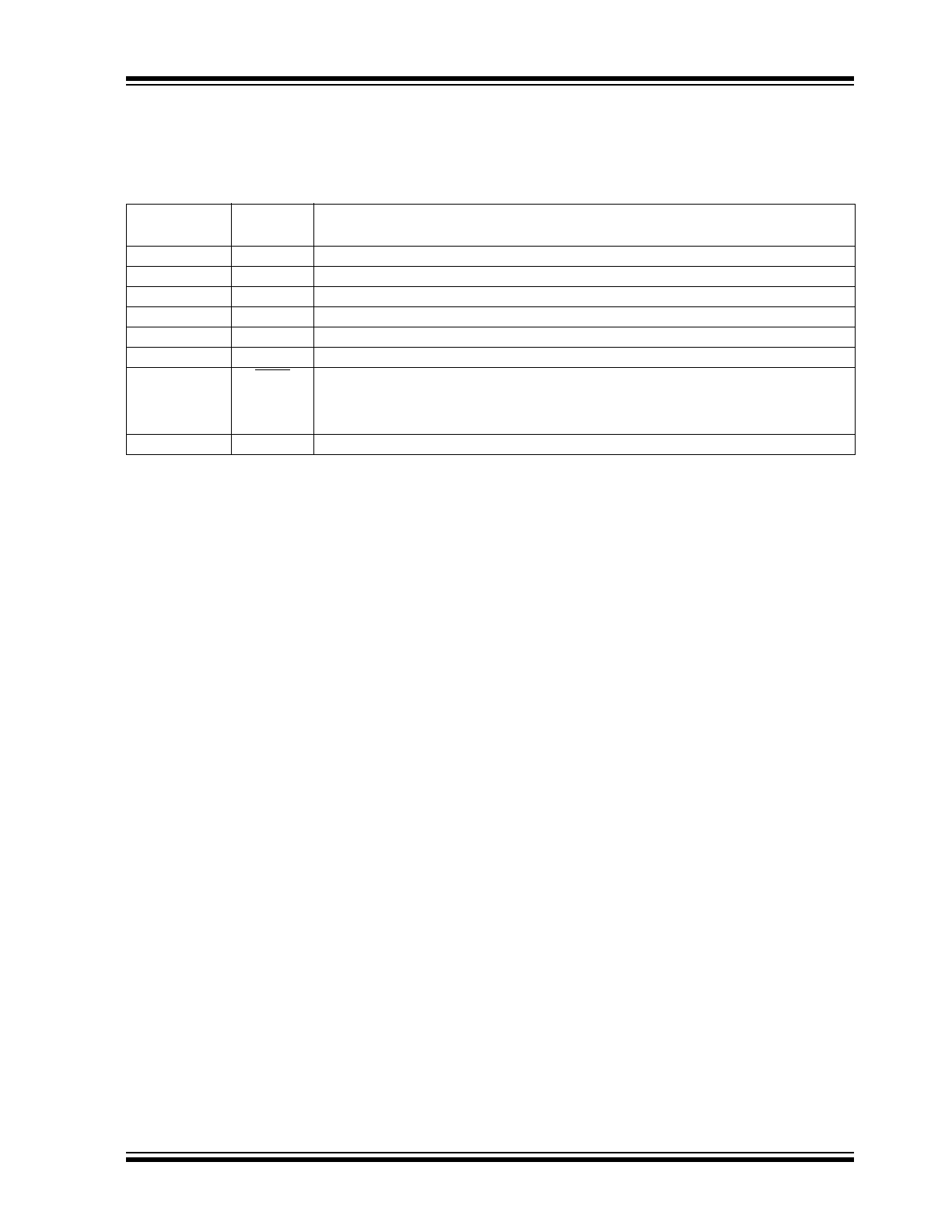
PIN DESCRIPTIONS
The descriptions of the pins are listed in Table 2-1.
TABLE 2-1:
PIN FUNCTION TABLE
Pin No.
(8-Pin SOIC)
Symbol
Description
1
V
OUT
Regulated voltage output.
2
NC
No connect.
3
NC
No connect.
4
GND
Ground terminal.
5
Bypass
Reference bypass input. Connecting a 470pF to this input further reduces output noise.
6
NC
No connect.
7
SHDN
Shutdown control input. The regulator is fully enabled when a logic high is applied to this input.
The regulator is fully enabled when a logic high is applied to this input. The regulator enters shut-
down when a logic low is applied to this input. During shutdown, output voltage falls to zero and
supply current is reduced to 0.05
A (typical).
8
V
IN
Unregulated supply input.
TC1269
DS21380C-page 4
2002-2012 Microchip Technology Inc.
3.0
DETAILED DESCRIPTION
The TC1269 is a precision regulator available in fixed
voltages. Unlike the bipolar regulators, the TC1269
supply current does not increase with load current. In
addition, V
OUT
remains stable and within regulation
over the entire 0mA to I
OUT
MAX
operating load current
range, (an important consideration in RTC and CMOS
RAM battery backup applications).
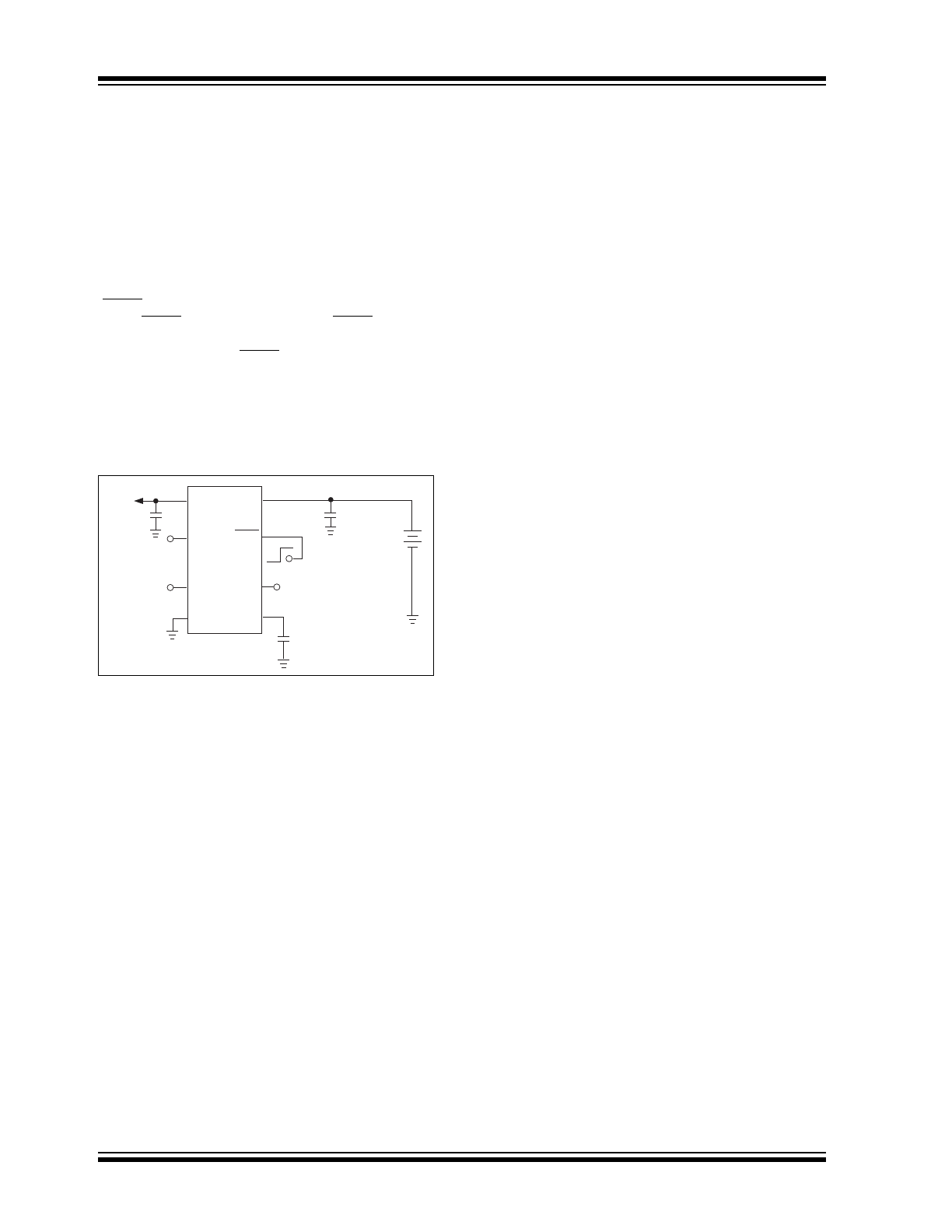
Figure 3-1 shows a typical application circuit. The
regulator is enabled any time the shutdown input
(SHDN) is at or above V
IH
, and shutdown (disabled)
when SHDN is at or below V
IL
. SHDN may be
controlled by a CMOS logic gate, or I/O port of a
microcontroller. If the SHDN input is not required, it
should be connected directly to the input supply. While
in shutdown, supply current decreases to 0.05
A
(typical), V
OUT
falls to zero.
FIGURE 3-1:
TYPICAL APPLICATION
CIRCUIT
3.1
Bypass Input
A 470pF capacitor connected from the Bypass input to
ground reduces noise present on the internal
reference, which in turn significantly reduces output
noise. If output noise is not a concern, this input may be
left unconnected. Larger capacitor values may be
used, but results in a longer time period to rated output
voltage when power is initially applied.
3.2
Output Capacitor
A 1
F (min) capacitor from V
OUT
to ground is
recommended. The output capacitor should have an
effective series resistance greater than 0.1
and less
than 5.0
, and a resonant frequency above 1MHz. A
1
F capacitor should be connected from V
IN
to GND if
there is more than 10 inches of wire between the
regulator and the AC filter capacitor, or if a battery is
used as the power source. Aluminum electrolytic or
tantalum capacitor types can be used. (Since many
aluminum electrolytic capacitors freeze at approxi-
mately -30°C, solid tantalums are recommended for
applications operating below -25°C.) When operating
from sources other than batteries, supply-noise
rejection and transient response can be improved by
increasing the value of the input and output capacitors
and employing passive filtering techniques.
TC1269
1
2
3
4
6
7
8
NC
NC
GND
Bypass
NC
SHDN
Battery
V
OUT
V
OUT
C
BYPASS
470pF
(Optional)
Shutdown Control
(from Power
Control Logic)
C1
1
µF
V
IN
+
C1
1
µF
+
+
–
2002-2012 Microchip Technology Inc.
DS21380C-page 5
TC1269
4.0
THERMAL CONSIDERATIONS
4.1
Thermal Shutdown
Integrated thermal protection circuitry shuts the
regulator off when die temperature exceeds 150°C.
The regulator remains off until the die temperature
drops to approximately 140°C.
4.2
Power Dissipation
The amount of power the regulator dissipates is
primarily a function of input and output voltage, and
output current. The following equation is used to
calculate worst case actual power dissipation:
EQUATION 4-1:
The maximum allowable power dissipation
(Equation 4-2) is a function of the maximum ambient
temperature (T
A
MAX
), the maximum allowable die
temperature (T
J
MAX
) and the thermal resistance from
junction-to-air (
JA
).
EQUATION 4-2:
Equation 4-1 can be used in conjunction with
Equation 4-2 to ensure regulator thermal operation is
within limits. For example:
Given:
V
IN
MAX
= 3.0V ± 10%
V
OUT
MIN
= 2.7V – 2.5%
I
LOAD
= 250mA
T
A
MAX
= 55°C
Find: 1. Actual power dissipation
2. Maximum allowable dissipation
Actual power dissipation:
P
D
(V
IN
MAX
– V
OUT
MIN
)
I
LOAD
MAX
= [(3.0 x 1.1) – (2.7 x .975)]250 x 10
-3
= 167mW
Maximum allowable power dissipation:
In this example, the TC1269 dissipates a maximum of
167mW; below the allowable limit of 350mW. In a
similar manner, Equation 4-1 and Equation 4-2 can be
used to calculate maximum current and/or input
voltage limits.
4.3
Layout Considerations
The primary path of heat conduction out of the package
is via the package leads. Therefore, layouts having a
ground plane, wide traces at the pads, and wide power
supply bus lines combine to lower
JA
and, therefore,
increase the maximum allowable power dissipation
limit.
Where:
P
D
(V
IN
MAX
– V
OUT
MIN
)I
LOAD
MAX
P
D
V
IN
MAX
V
OUT
MIN
I
LOAD
MAX
= Worst case actual power dissipation
= Minimum regulator output voltage
= Maximum output (load) current
= Maximum voltage on V
IN
P
D
MAX
= (T
J
MAX
– T
A
MAX
)
JA
Where all terms are previously defined.
P
D
MAX
= (T
J
MAX
– T
A
MAX
)
JA
= (125 – 55)
200
= 350mW
TC1269
DS21380C-page 6
2002-2012 Microchip Technology Inc.
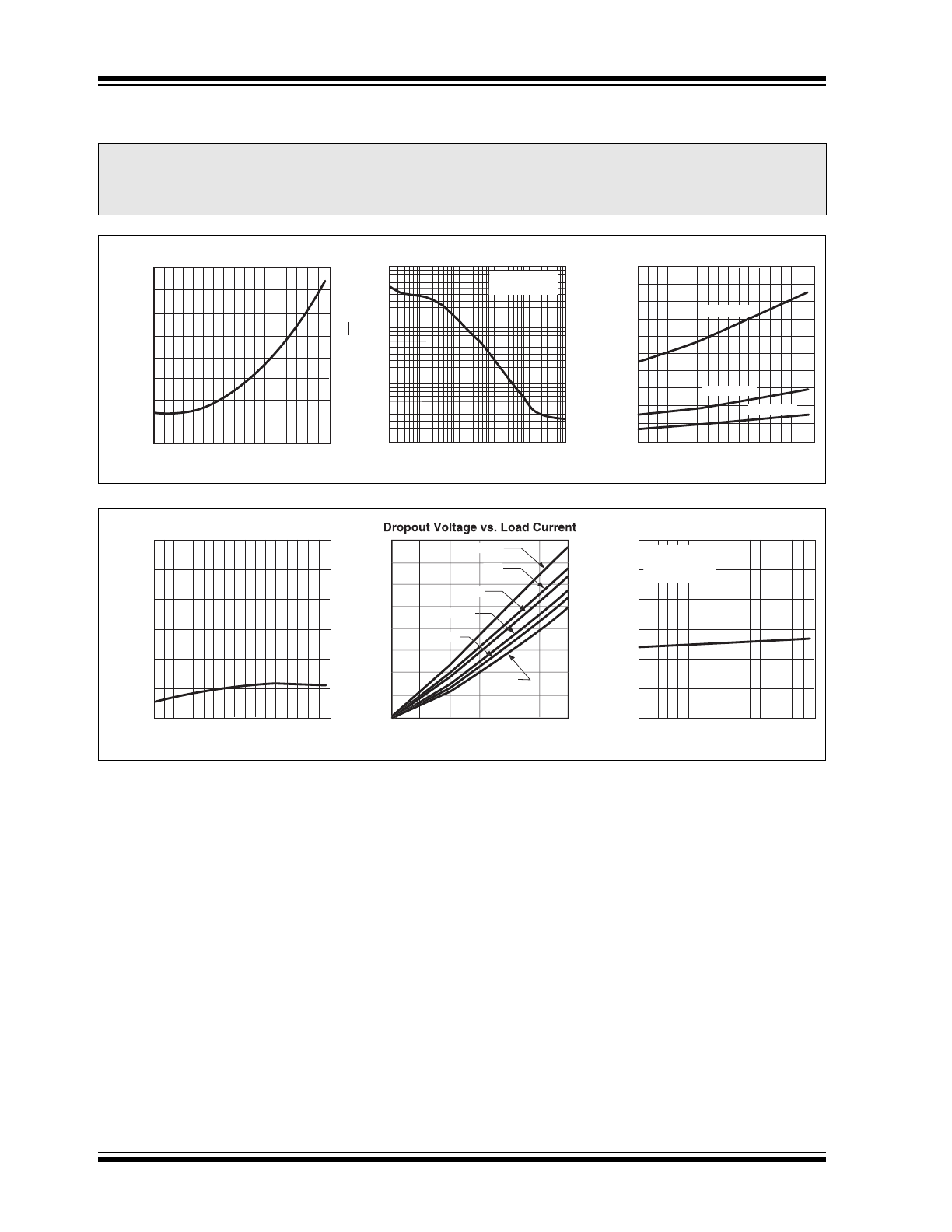
5.0
TYPICAL CHARACTERISTICS
Note:
The graphs and tables provided following this note are a statistical summary based on a limited number of
samples and are provided for informational purposes only. The performance characteristics listed herein are
not tested or guaranteed. In some graphs or tables, the data presented may be outside the specified
operating range (e.g., outside specified power supply range) and therefore outside the warranted range.
Output Noise
FREQUENCY (kHz)
NOISE (
μ
V/
√
HZ)
10.0
1.0
0.01
0.01
1
10
100
1000
0.1
0.0
R
LOAD
= 50Ω
C
OUT
= 1
μF
0.012
0.010
0.008
0.004
0.002
0.000
-0.002
-0.004
0.006
-40
° -20° 0° 20° 40° 60° 80° 100° 120°
TEMPERATURE (
°
C)
Line Regulation
LINE REGULATION (%)
2.00
1.80
1.60
1.20
1.00
0.80
0.60
0.40
0.20
0.00
1.40
-40
° -20° 0° 20° 40° 60° 80° 100° 120°
TEMPERATURE (
°
C)
Load Regulation
LOAD REGULATION (%)
1 to 300mA
1 to 50mA
1 to 100mA
0.40
0.35
0.30
0.25
0.20
0.15
0.10
0.05
0.00
0
50
100
150
200
250
300
LOAD CURRENT (mA)
DROPOUT VOLTAGE (V)
100.0
90.0
70.0
80.0
50.0
40.0
60.0
-40
° -20° 0° 20° 40° 60° 80° 100° 120°
TEMPERATURE (
°C)
Supply Current
SUPPLY CURRENT (
μ
A)
3.075
3.025
2.925
2.975
-40
° -20° 0° 20° 40° 60° 80° 100° 120°
TEMPERATURE (
°C)
V
OUT
vs. Temperature
V
OUT
(V)
125
°C
8
85
°C
C
70
°C
25
°C
0
°C
C
-40
°C
V
IN
= 4V
I
LOAD
= 100μA
C
LOAD
= 3.3
μF
2002-2012 Microchip Technology Inc.
DS21380C-page 7
TC1269
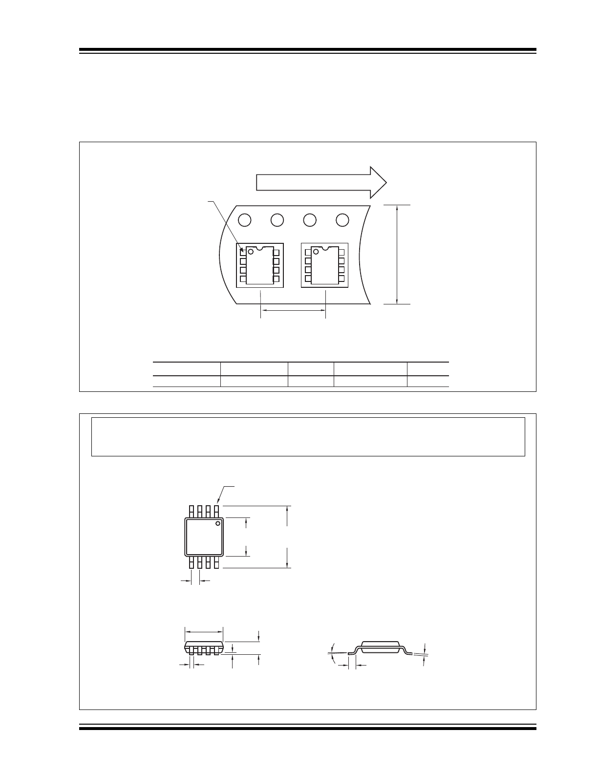
6.0
PACKAGING INFORMATION
6.1
Package Marking Information
Package marking data not available at this time.
6.2
Taping Form
6.3
Package Dimensions
Component Taping Orientation for 8-Pin MSOP Devices
Package
Carrier Width (W)
Pitch (P)
Part Per Full Reel
Reel Size
8-Pin MSOP
12 mm
8 mm
2500
13 in
Carrier Tape, Number of Components Per Reel and Reel Size
PIN 1
User Direction of Feed
Standard Reel Component Orientation
for TR Suffix Device
W
P
8-Pin MSOP
.122 (3.10)
.114 (2.90)
.122 (3.10)
.114 (2.90)
.043 (1.10)
MAX.
.006 (0.15)
.002 (0.05)
.016 (0.40)
.010 (0.25)
.197 (5.00)
.189 (4.80)
.008 (0.20)
.005 (0.13)
.028 (0.70)
.016 (0.40)
6
° MAX.
.026 (0.65) TYP.
PIN 1
Dimensions: inches (mm)
Note:
For the most current package drawings, please see the Microchip Packaging Specification located
at http://www.microchip.com/packaging

TC1269
DS21380C-page 8
2002-2012 Microchip Technology Inc.
7.0
REVISION HISTORY
Revision C (November 2012)
Added a note to each package outline drawing.

2002-2012 Microchip Technology Inc.
DS21380C-page 9
TC1269
SALES AND SUPPORT
Data Sheets
Products supported by a preliminary Data Sheet may have an errata sheet describing minor operational differences and recom-
mended workarounds. To determine if an errata sheet exists for a particular device, please contact one of the following:
1.
Your local Microchip sales office
2.
The Microchip Worldwide Site (www.microchip.com)
Please specify which device, revision of silicon and Data Sheet (include Literature #) you are using.
New Customer Notification System
Register on our web site (www.microchip.com/cn) to receive the most current information on our products.

TC1269
DS21380C-page 10
2002-2012 Microchip Technology Inc.
NOTES: