
2002-2012 Microchip Technology Inc.
DS21374D-page 1
TC1263
Features
• Very Low Dropout Voltage
• 500 mA Output Current
• High-Output Voltage Accuracy
• Standard or Custom Output Voltages
• Overcurrent and Overtemperature Protection
• SHDN Input for Active Power Management
• ERROR Output Can Be Used as a Low Battery
Detector (SOIC only)
Applications
• Battery-Operated Systems
• Portable Computers
• Medical Instruments
• Instrumentation
• Cellular/GSM/PHS Phones
• Linear Post-Regulators for SMPS
• Pagers
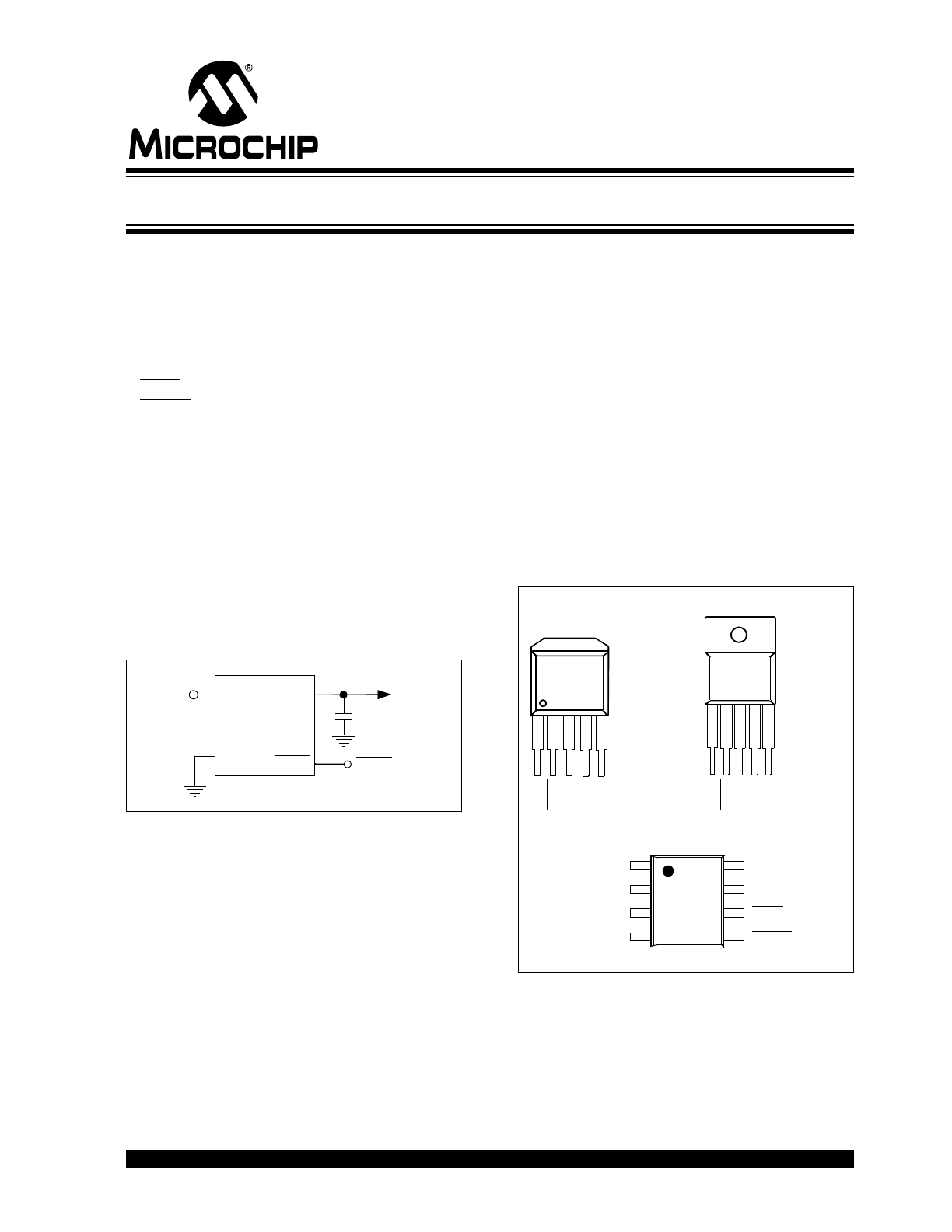
Typical Application
Description
The TC1263 is a fixed-output, high-accuracy (typically
±0.5%) CMOS low dropout regulator. Designed
specifically for battery-operated systems, the TC1263’s
CMOS construction eliminates wasted ground current,
significantly extending battery life. Total supply current
is typically 80 µA at full load (20 to 60 times lower than
in bipolar regulators).
TC1263 key features include ultra low noise operation,
very low dropout voltage (typically 350 mV at full load)
and fast response to step changes in load.
The TC1263 incorporates both overtemperature and
overcurrent protection. The TC1263 is stable with an
output capacitor of only 1 µF and has a maximum
output current of 500 mA. It is available in 8-Pin SOIC,
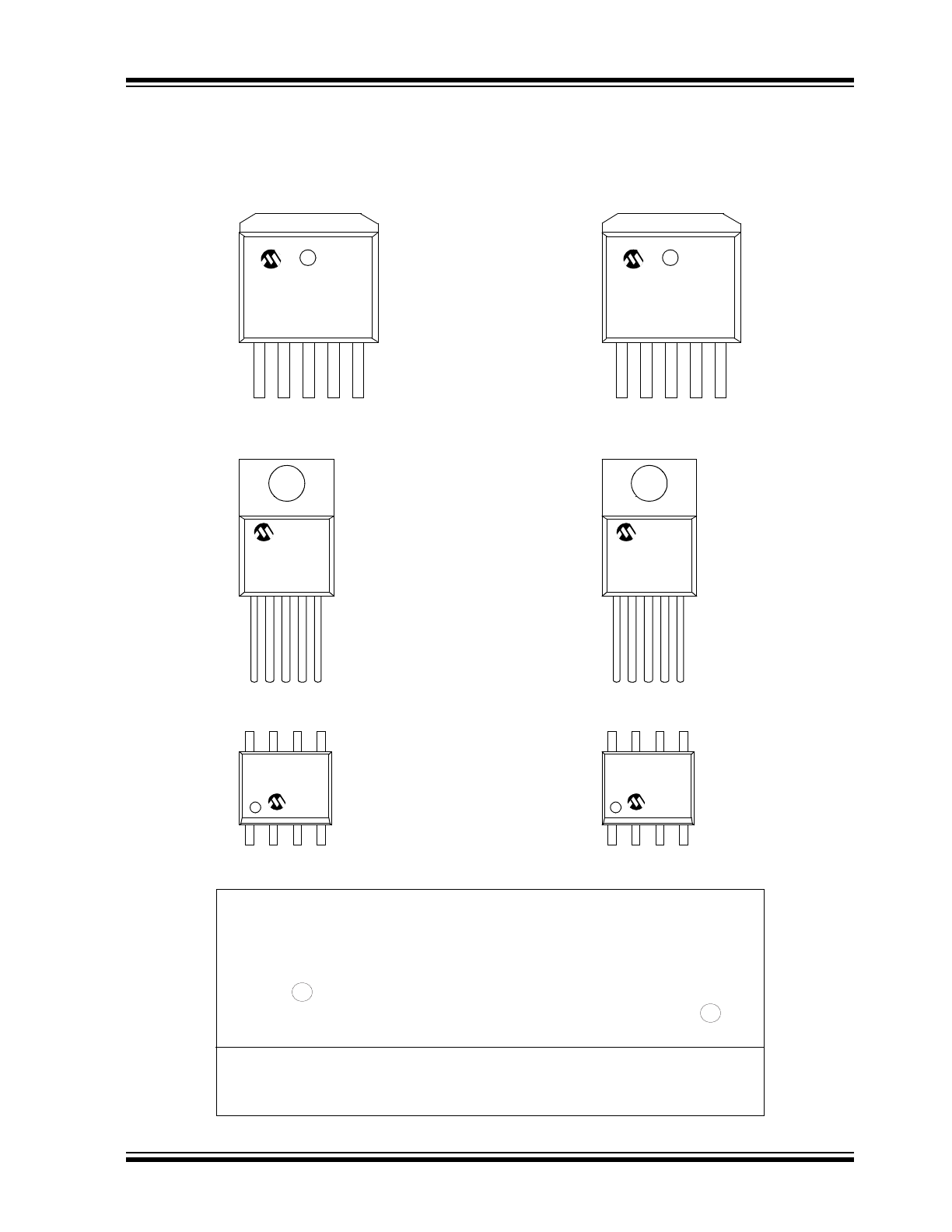
5-Pin TO-220 and 5-Pin DDPAK packages.
Package Type
TC1263
V
IN
V
OUT
C
1
1 µF
GND
V
OUT
V
IN
SHDN
SHDN
+
V
IN
GND
V
OU
T
Front View
1 2
3
Tab is GND
TC1263
1
2
3
4
8
7
6
5
TC1263
NC
SHDN
8-Pin SOIC
GND
NC
BYPASS
V
OUT
V
IN
V
IN
V
OU
T
TC1263
5-Pin TO-220
Tab is GND
5-Pin DDPAK
1 2 3
GND
SH
D
N
4 5
BY
P
BYP
4
SHDN
5
ERROR
500 mA, Fixed-Output, CMOS LDO with Shutdown
TC1263
DS21374D-page 2
2002-2012 Microchip Technology Inc.
1.0
ELECTRICAL
CHARACTERISTICS
Absolute Maximum Ratings †
Input Voltage .........................................................6.5V
Output Voltage................ (GND
– 0.3V) to (V
IN
+ 0.3V)
Power Dissipation................Internally Limited (Note 7)
Voltage (max.) on Any Pin: (GND
– 0.3V) to (V
IN
+ 0.3V)
Operating Temperature Range.... -40°C < T
J
< +125°C
Storage Temperature..........................-65°C to +150°C
† Notice: Stresses above those listed under "Maximum
Ratings" may cause permanent damage to the device. This is
a stress rating only and functional operation of the device at
those or any other conditions above those indicated in the
operation listings of this specification is not implied. Exposure
to maximum rating conditions for extended periods may affect
device reliability.
DC CHARACTERISTICS
Electrical Specifications: Unless otherwise indicated, V
IN
= V
R
+ 1.0V, (Note 1), I
L
= 100 µA, C
L
= 3.3 µF,
SHDN > V
IH
, T
A
= +25°C. Boldface type specifications apply for junction temperatures of -40°C to +125°C.
Parameters
Sym
Min
Typ
Max
Units
Conditions
Input Operating Voltage
V
IN
2.7
—
6.0
V
Note 2
Maximum Output Current
I
OUTMAX
500
—
—
mA
Output Voltage
V
OUT
V
R
– 2.5%
V
R
± 0.5% V
R
+ 2.5%
V
Note 1
V
OUT
Temperature Coefficient
V
OUT
/
T
—
40
—
ppm/°C Note 3
Line Regulation
V
OUT
/
V
IN
—
0.05
0.35
%
(V
R
+ 1V)
V
IN
6V
Load Regulation (Note 4)
V
OUT
/V
OUT
–0.01
0.002
+0.01
%/mA
I
L
= 0.1 mA to I
OUTMAX
Dropout Voltage (Note 5)
V
IN
-V
OUT
—
20
30
mV
I
L
= 100 µA
—
60
130
I
L
= 100 mA
—
200
390
I
L
= 300 mA
—
350
650
I
L
= 500 mA
Supply Current
I
DD
—
80
130
µA
SHDN = V
IH
, I
L
= 0
Shutdown Supply Current
I
SHDN
—
0.05
1
µA
SHDN = 0V
Power Supply Rejection Ratio
PSRR
—
64
—
db
F
1 kHz
Output Short Circuit Current
I
OUTSC
—
1200
1400
mA
V
OUT
= 0V
Thermal Regulation
V
OUT
/
P
D
—
0.04
—
V/W
Note 6
Output Noise
eN
—
260
—
nV/
Hz I
L
= I
OUTMAX
, F = 10 kH
Z
Note
1:
V
R
is the regulator output voltage setting.
2:
The minimum V
IN
has to justify the conditions: V
IN
V
R
+ V
DROPOUT
and V
IN
2.7V for I
L
= 0.1 mA to I
OUTMAX
.
3:
4:
Regulation is measured at a constant junction temperature using low duty-cycle pulse testing. Load regulation is tested
over a load range from 0.1 mA to the maximum specified output current. Changes in output voltage due to heating
effects are covered by the thermal regulation specification.
5:
Dropout voltage is defined as the input-to-output differential at which the output voltage drops 2% below its nominal
value measured at a 1.0V differential.
6:
Thermal regulation is defined as the change in output voltage at a time T after a change in power dissipation is applied,
excluding load or line regulation effects. Specifications are for a current pulse equal to I
LMAX
at V
IN
= 6V for T = 10 ms.
7:
The maximum allowable power dissipation is a function of ambient temperature, the maximum allowable junction
temperature and the thermal resistance from junction-to-air (i.e., T
A
, T
J
,
JA
). Exceeding the maximum allowable power
dissipation causes the device to initiate thermal shutdown. Please see Section 5.0 “Thermal Considerations” for
more details.
TCV
OUT
V
OUTMAX
V
OUTMIN
–
10
6
–
V
OUT
T
-------------------------------------------------------------------------
=
2002-2012 Microchip Technology Inc.
DS21374D-page 3
TC1263
SHDN Input
SHDN Input High Threshold
V
IH
45
—
—
%V
IN
SHDN Input Low Threshold
V
IL
—
—
15
%V
IN
ERROR Output (SOIC Only)
Minimum Operating Voltage
V
MIN
1.0
—
—
V
Output Logic Low Voltage
V
OL
—
—
400
mV
1 mA Flows to ERROR
ERROR Threshold Voltage
V
TH
—
0.95 x V
R
—
V
ERROR Positive Hysteresis
V
HYS
—
50
—
mV
DC CHARACTERISTICS (CONTINUED)
Electrical Specifications: Unless otherwise indicated, V
IN
= V
R
+ 1.0V, (Note 1), I
L
= 100 µA, C
L
= 3.3 µF,
SHDN > V
IH
, T
A
= +25°C. Boldface type specifications apply for junction temperatures of -40°C to +125°C.
Parameters
Sym
Min
Typ
Max
Units
Conditions
Note
1:
V
R
is the regulator output voltage setting.
2:
The minimum V
IN
has to justify the conditions: V
IN
V
R
+ V
DROPOUT
and V
IN
2.7V for I
L
= 0.1 mA to I
OUTMAX
.
3:
4:
Regulation is measured at a constant junction temperature using low duty-cycle pulse testing. Load regulation is tested
over a load range from 0.1 mA to the maximum specified output current. Changes in output voltage due to heating
effects are covered by the thermal regulation specification.
5:
Dropout voltage is defined as the input-to-output differential at which the output voltage drops 2% below its nominal
value measured at a 1.0V differential.
6:
Thermal regulation is defined as the change in output voltage at a time T after a change in power dissipation is applied,
excluding load or line regulation effects. Specifications are for a current pulse equal to I
LMAX
at V
IN
= 6V for T = 10 ms.
7:
The maximum allowable power dissipation is a function of ambient temperature, the maximum allowable junction
temperature and the thermal resistance from junction-to-air (i.e., T
A
, T
J
,
JA
). Exceeding the maximum allowable power
dissipation causes the device to initiate thermal shutdown. Please see Section 5.0 “Thermal Considerations” for
more details.
TCV
OUT
V
OUTMAX
V
OUTMIN
–
10
6
–
V
OUT
T
-------------------------------------------------------------------------
=
TEMPERATURE CHARACTERISTICS
Electrical Specifications: Unless otherwise indicated, V
IN
= V
R
+ 1.0V, I
L
= 100 µA, C
L
= 3.3 µF,
SHDN > V
IH
, T
A
= +25°C.
Parameters
Sym
Min
Typ
Max
Units
Conditions
Temperature Ranges
Specified Temperature Range
T
A
-40
—
+125
°C
Note 1
Operating Temperature Range
T
J
-40
—
+125
°C
Storage Temperature Range
T
A
-65
—
+150
°C
Thermal Package Resistances
Thermal Resistance, 5L-DDPAK
JA
—
57
—
°C/W
Thermal Resistance, 5L-TO-220
JA
—
71
—
°C/W
Thermal Resistance, 8L-SOIC
JA
—
163
—
°C/W
Note
1:
Operation in this range must not cause T
J
to exceed Maximum Junction Temperature (+125°C).
TC1263
DS21374D-page 4
2002-2012 Microchip Technology Inc.
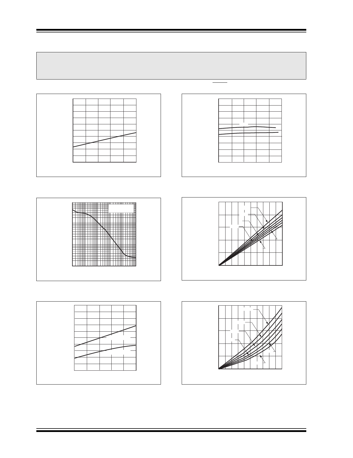
2.0
TYPICAL PERFORMANCE CURVES
Note: Unless otherwise indicated, V
IN
= V
R
+ 1.0V, I
L
= 100 µA, C
L
= 3.3 µF, SHDN > V
IH
, T
A
= +25°C.
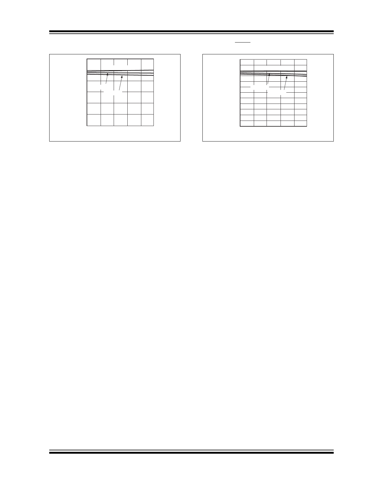
FIGURE 2-1:
Line Regulation vs.
Temperature.
FIGURE 2-2:
Output Noise vs. Frequency.
FIGURE 2-3:
Load Regulation vs.
Temperature.
FIGURE 2-4:
I
DD
vs. Temperature.
FIGURE 2-5:
2.5V Dropout Voltage vs.
I
LOAD
.
FIGURE 2-6:
5.0V Dropout Voltage vs.
I
LOAD
.
Note:
The graphs and tables provided following this note are a statistical summary based on a limited number of
samples and are provided for informational purposes only. The performance characteristics listed herein
are not tested or guaranteed. In some graphs or tables, the data presented may be outside the specified
operating range (e.g., outside specified power supply range) and therefore outside the warranted range.
0.020
0.018
0.016
0.012
0.010
0.008
0.006
0.004
0.002
0.000
0.014
TEMPERATURE (°C)
LI
N
E
R
EG
U
LA
TIO
N
(%
)
-40°C 0°C
25°C 70°C
85°C 125°C
FREQUENCY (
kHz)
N
OISE
(μ
V/
√H
z)
10.0
1.0
0.01
0.01
1
10
100
1000
0.1
0.0
R
LOAD
= 50Ω
C
OUT
= 1μF
-40
°C
0
°C
25
°C 70°C
85
°C 125°C
0.0100
0.0090
0.0080
0.0070
0.0060
0.0050
0.0040
0.0030
0.0020
0.0010
0.0100
TEMPERATURE (
°C)
LOAD REGULATION (%/mA)
1mA to 500mA
1mA to 500mA
5V
2.5V
TEMPERATURE (°C)
I
DD
(μ
A
)
150
135
120
105
90
75
60
45
30
15
0
5V
-40°C 0°C
25°C 70°C
85°C 125°C
2.5V
0
100
200
300
400
500
I
LOAD
(
mA)
DR
OPO
U
T VOLT
A
GE
(V
)
0.50
0.40
0.30
0.20
0.10
0.00
-40°C
0°C
70°C
85°C
25°C
125°C
0
100
200
300
400
500
I
LOAD
(
mA)
0.50
0.40
0.30
0.20
0.10
0.00
DR
OPO
U
T VOLT
A
GE
(V
)
25°C
-40°C
0°C
70°C
85°C
125°C
2002-2012 Microchip Technology Inc.
DS21374D-page 5
TC1263
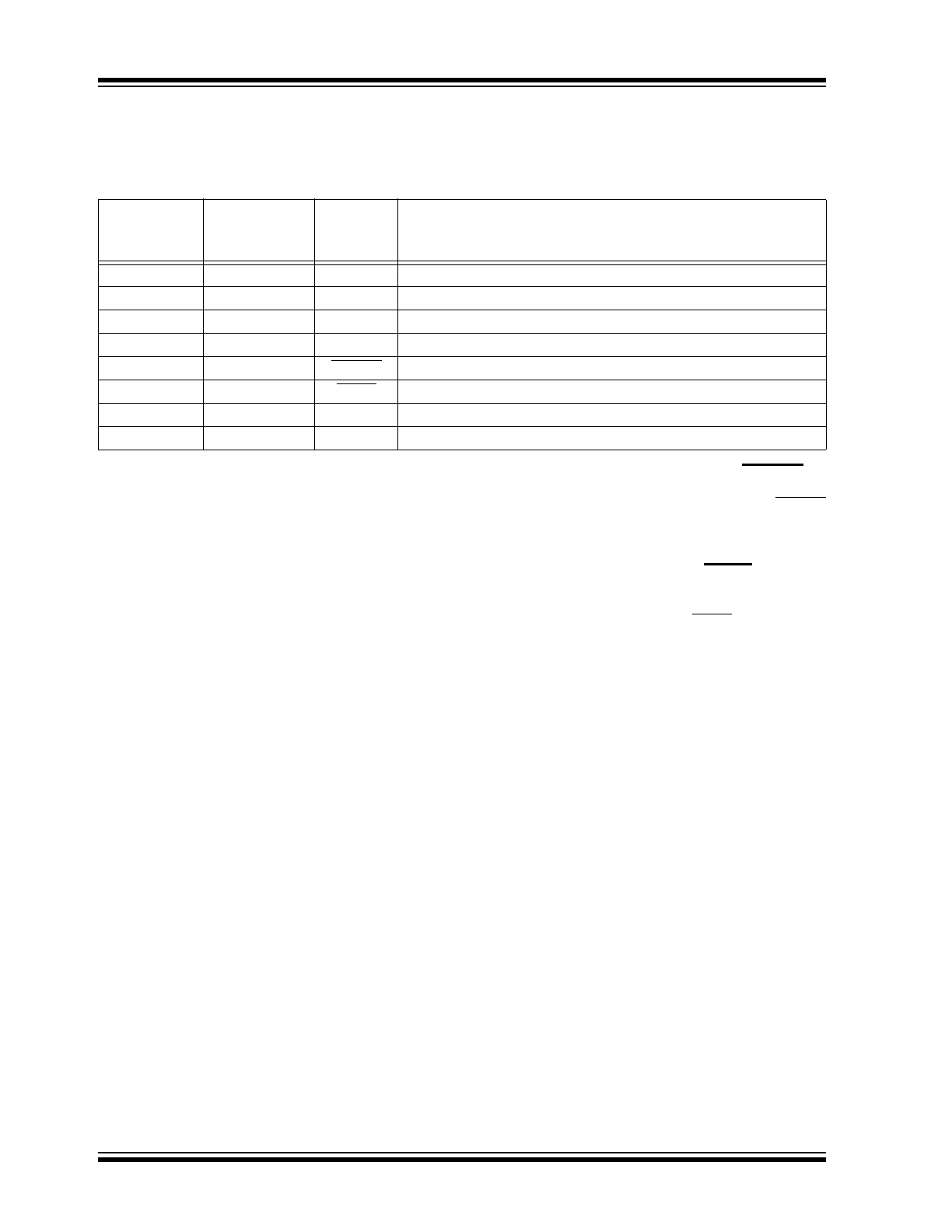
Note: Unless otherwise indicated, V
IN
= V
R
+ 1.0V, I
L
= 100 µA, C
L
= 3.3 µF, SHDN > V
IH
, T
A
= +25°C.
FIGURE 2-7:
2.5V V
OUT
vs. Temperature.
FIGURE 2-8:
5.0V V
OUT
vs. Temperature.
2.70
2.50
2.30
2.10
1.90
1.70
1.50
-40°C
0°C
25°C
70°C
85°C 125°C
TEMPERATURE (°C)
I
L
= 0.1
mA
I
L
= 300
mA
I
L
= 500
mA
V
O
U
T
(V
)
5.20
5.10
5.00
4.90
4.80
4.70
4.60
4.50
4.40
4.30
4.20
4.10
4.00
-40°C
0°C
25°C
70°C
85°C 125°C
TEMPERATURE (°C)
V
O
U
T
(V
)
I
L
= 0.1
mA
I
L
= 300
mA
I
L
= 500
mA
TC1263
DS21374D-page 6
2002-2012 Microchip Technology Inc.
3.0
PIN DESCRIPTIONS
The descriptions of the pins are listed in Table 3-1.
TABLE 3-1:
PIN FUNCTION TABLE
3.1
Regulated Output Voltage (V
OUT
)
V
OUT
is a regulated voltage output.
3.2
Ground (GND)
Ground terminal.
3.3
Reference Bypass (BYPASS)
Reference bypass input. Connect a 470 pF to the
BYPASS input to further reduce output noise.
3.4
Out-of-Regulation Flag (ERROR)
Out-of-Regulation Flag (open-drain output). ERROR
goes low when V
OUT
is out-of-tolerance by
approximately – 5%.
3.5
Shutdown Control (SHDN)
Shutdown control input. The regulator is fully enabled
when a logic-high is applied to SHDN. The regulator
enters shutdown when a logic-low is applied to this
input. During shutdown, output voltage falls to zero and
supply current is reduced to 0.05 µA (typical).
3.6
Unregulated Supply (V
IN
)
V
IN
is an unregulated supply input.
Pin No.
(8-Pin SOIC)
Pin No.
(5-Pin DDPAK)
(5-Pin TO-220)
Symbol
Description
1
5
V
OUT
Regulated voltage output
2
3
GND
Ground terminal
3
—
NC
No connect
4
1
BYPASS
Reference bypass input
5
—
ERROR
Out-of-Regulation Flag (open-drain output).
6
2
SHDN
Shutdown control input
7
—
NC
No connect
8
4
V
IN
Unregulated supply input
2002-2012 Microchip Technology Inc.
DS21374D-page 7
TC1263
4.0
DETAILED DESCRIPTION
The TC1263 is a precision, fixed-output LDO. Unlike
bipolar regulators, the TC1263’s supply current does
not increase with load current. In addition, V
OUT
remains stable and within regulation over the entire
0 mA to I
LOADMAX
load current range (an important
consideration in RTC and CMOS RAM battery back-up
applications).
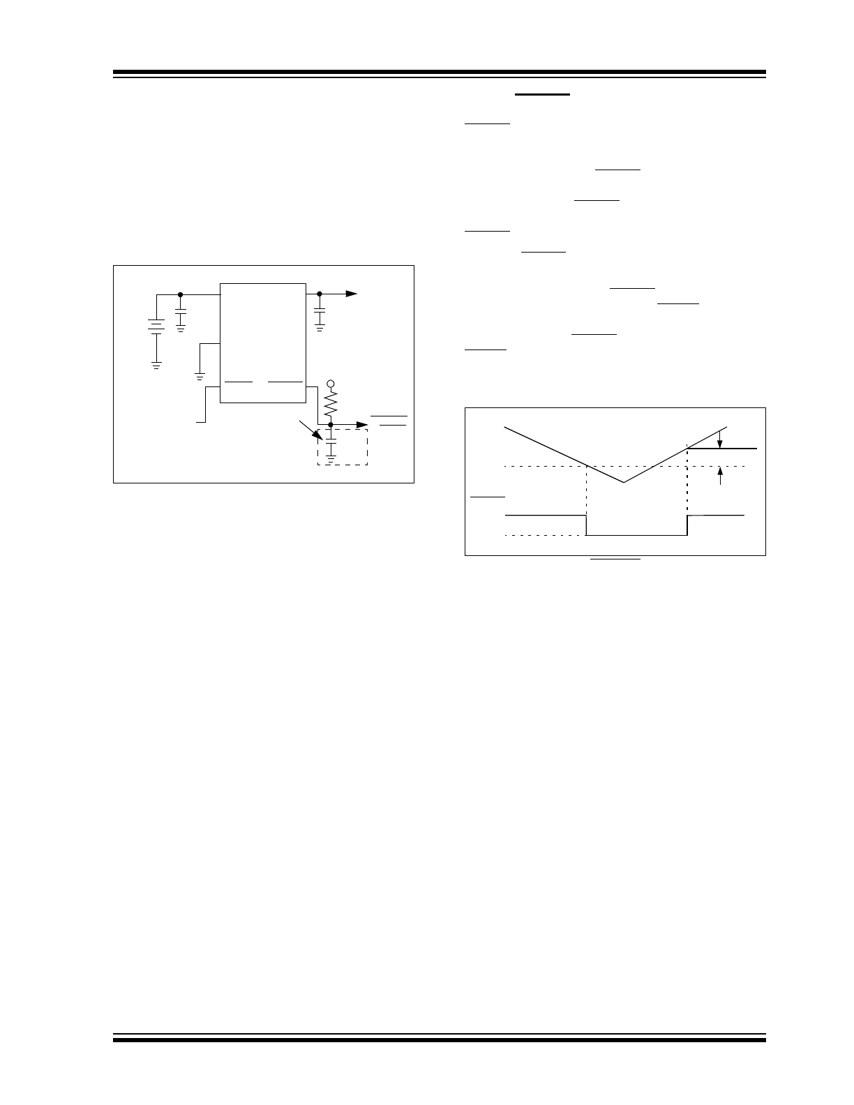
Figure 4-1 shows a typical application circuit.
FIGURE 4-1:
Typical Application Circuit.
4.1
Output Capacitor
A 1 µF (min.) capacitor from V
OUT
to ground is
required. The output capacitor should have an Effective
Series Eesistance (ESR) greater than 0.1
and less
than 5
. A 1 µF capacitor should be connected from
V
IN
to GND if there is either more than 10 inches of wire
between the regulator and the AC filter capacitor or a
battery is used as the power source. Aluminum
electrolytic or tantalum capacitor types can be used.
Since many aluminum electrolytic capacitors freeze at
approximately -30°C, solid tantalums are
recommended for applications operating below -25°C.
When operating from sources other than batteries,
supply-noise rejection and transient response can be
improved by increasing the value of the input and
output capacitors, and by employing passive filtering
techniques.
4.2
ERROR Output
ERROR is driven low whenever V
OUT
falls out of
regulation by more than – 5% (typ.). This condition may
be caused by low input voltage, output current limiting
or thermal limiting. The ERROR threshold is 5% below
rated V
OUT
, regardless of the programmed output
voltage value (e.g., ERROR = V
OL
at 4.75V (typ.) for a
5.0V regulator and 2.85V (typ.) for a 3.0V regulator).
ERROR output operation is shown in Figure 4-2.
Note that ERROR is active when V
OUT
is at or below
V
TH
, and inactive when V
OUT
is above V
TH
+ V
HYS
.
As shown in Figure 4-1, ERROR can be used as a
battery-low flag or as a processor RESET signal (with
the addition of timing capacitor C
3
). R
1
x C
3
should be
chosen to maintain ERROR below V
IH
of the processor
RESET input for at least 200 ms to allow time for the
system to stabilize. Pull-up resistor R
1
can be tied to
V
OUT
, V
IN
or any other voltage less than (V
IN
+ 0.3V).
FIGURE 4-2:
ERROR Output Operation.
C
1
R
1
1 M
V
+
TC1263
V
IN
Battery
V
OUT
ERROR
SHDN
GND
V
OUT
1 µF
+
+
Shutdown Control
(to CMOS Logic or Tie
to V
IN
, if unused)
C
2
1 µF
+
C
3
Required Only
if ERROR is used as a
Processor RESET Signal
(See Text)
C
3
0.2 µF
+
BATTLOW
or RESET
V
OUT
V
TH
V
OH
Hysteresis (V
HYS
)
V
OL
ERROR
TC1263
DS21374D-page 8
2002-2012 Microchip Technology Inc.
5.0
THERMAL CONSIDERATIONS
5.1
Thermal Shutdown
Integrated thermal protection circuitry shuts the
regulator off when the die temperature exceeds 160°C.
The regulator remains off until the die temperature
drops to approximately 150°C.
5.2
Power Dissipation
The amount of power the regulator dissipates is
primarily a function of input and output voltage and out-
put current. The following equation is used to calculate
worst-case actual power dissipation:
EQUATION 5-1:
The maximum allowable power dissipation
(Equation 5-2) is a function of the maximum ambient
temperature (T
AMAX
), the maximum allowable die
temperature (T
JMAX
) and the thermal resistance from
junction-to-air (
JA
).
EQUATION 5-2:
Table 5-1 and Table 5-2 show various values of
JA
for
the TC1263 package types.
TABLE 5-1:
THERMAL RESISTANCE
GUIDELINES FOR TC1263 IN
8-PIN SOIC PACKAGE
TABLE 5-2:
THERMAL RESISTANCE
GUIDELINES FOR TC1263 IN
5-PIN DDPAK/TO-220
PACKAGE
Equation 5-1 can be used in conjunction with
Equation 5-2 to ensure regulator thermal operation is
within limits. For example:
Find:
1.
Actual power dissipation
2.
Maximum allowable dissipation
Actual power dissipation:
Maximum allowable power dissipation:
In this example, the TC1263 dissipates a maximum of
260 mW below the allowable limit of 500 mW. In a
similar manner, Equation 5-1 and Equation 5-2 can be
used to calculate maximum current and/or input
voltage limits. For example, the maximum allowable
V
IN
is found by substituting the maximum allowable
power dissipation of 500 mW into Equation 5-1, from
which V
INMAX
= 4.6V.
Copper
Area
(Topside)*
Copper
Area
(Backside)
Board
Area
Thermal
Resistance
JA
)
2500 sq mm
2500 sq mm 2500 sq mm
60°C/W
1000 sq mm
2500 sq mm 2500 sq mm
60°C/W
225 sq mm
2500 sq mm 2500 sq mm
68°C/W
100 sq mm
2500 sq mm 2500 sq mm
74°C/W
* Pin 2 is ground. Device is mounted on top-side.
Where:
V
INMAX
V
OUTMIN
I
LOADMAX
P
D
= Worst-case actual power dissipation
= Minimum regulator output voltage
= Maximum output (load) current
= Maximum voltage on V
IN
P
D
V
IN MAX
V
OUTMIN
–
I
LOA DMAX
=
Where:
V
INMAX
V
OUTMIN
I
LOADMAX
P
D
= Worst-case actual power dissipation
= Minimum regulator output voltage
= Maximum output (load) current
= Maximum voltage on V
IN
P
DMAX
T
JMAX
T
AMAX
–
JA
---------------------------------------
=
Copper
Area
(Topside)*
Copper
Area
(Backside)
Board
Area
Thermal
Resistance
JA
)
2500 sq mm
2500 sq mm 2500 sq mm
25°C/W
1000 sq mm
2500 sq mm 2500 sq mm
27°C/W
125 sq mm
2500 sq mm 2500 sq mm
35°C/W
* Tab of device attached to top-side copper
Given:
V
INMAX
=
3.3V ± 10%
V
OUTMIN
=
2.7V ± 0.5%
I
LOADMAX
=
275 mA
T
JMAX
=
125°C
T
AMAX
=
95°C
JA
=
60° C/W (SOIC)
P
D
V
INMAX
V
OUTMIN
–
I
LOADMAX
P
D
3.3
1.1
2.7
.995
–
275
10
3
–
=
P
D
260 mW
=
P
DMAX
T
JMAX
T
AMAX
–
JA
---------------------------------------
=
P
DMAX
125
95
–
60
-------------------------
=
P
DMAX
500 mW
=
2002-2012 Microchip Technology Inc.
DS21374D-page 9
TC1263
6.0
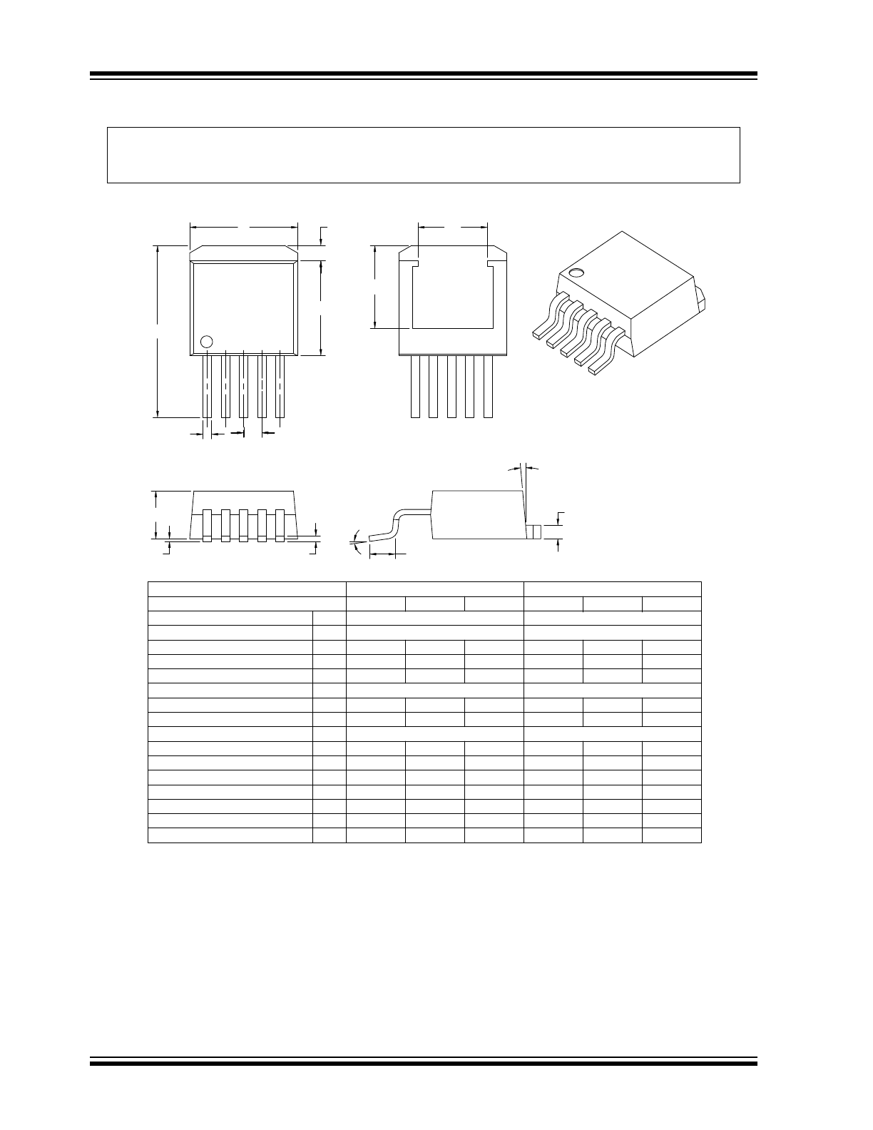
PACKAGING INFORMATION
6.1
Package Marking Information
XXXXXXXXX
XXXXXXXXX
YYWWNNN
5-Lead DDPAK
TC1263
3.3VET
Example:
5-Lead TO-220
XXXXXXXXX
XXXXXXXXX
YYWWNNN
Example:
TC1263-
3.3VAT
X
0430256
8-Lead SOIC (150 mil)
Example:
XXXXXXXX
XXXXYYWW
NNN
1263-3.3
VOA0430
256
0430256
Legend: XX...X
Customer-specific information
Y
Year code (last digit of calendar year)
YY
Year code (last 2 digits of calendar year)
WW
Week code (week of January 1 is week ‘01’)
NNN
Alphanumeric traceability code
Pb-free JEDEC designator for Matte Tin (Sn)
*
This package is Pb-free. The Pb-free JEDEC designator ( )
can be found on the outer packaging for this package.
Note:
In the event the full Microchip part number cannot be marked on one line, it will
be carried over to the next line, thus limiting the number of available
characters for customer-specific information.
3
e
3
e
TC1263
DS21374D-page 10
2002-2012 Microchip Technology Inc.
5-Lead Plastic (ET) (DDPAK)
BOTTOM VIEW
TOP VIEW
E
D
b
E1
D2
A
A1
c2
c
L
D1
e
θ1
θ
(5X)
L3
1
§ Significant Characteristic
Drawing No. C04-012
Notes:
Mold Draft Angle
Dimensions D and E do not include mold flash or protrusions. Mold flash or protrusions shall not
exceed .010" (0.254mm) per side.
θ1
7°
Pitch
Number of Pins
Overall Width
Standoff §
Molded Package Length
Exposed Pad Width
Overall Height
MAX
Units
Dimension Limits
A1
E1
D
E
e
A
.398
.000
.256 REF
INCHES*
.067 BSC
MIN
5
NOM
MAX
.010
0.00
10.11
6.50 REF
MILLIMETERS
.183
MIN
5
1.70 BSC
NOM
0.25
4.65
JEDEC equivalent: TO-252
4.50
.170
.005
0.13
Foot Length
L
.068
.089
.110
1.73
2.26
2.79
Foot Angle
θ
--
--
8°
.177
*Controlling Parameter
4.32
.385
.410
9.78
10.41
.330
.350
.370
8.38
8.89
9.40
Overall Length
D1
.549
.577
.605
13.94
14.66
15.37
Lead Thickness
c
.014
.020
.026
0.36
0.51
0.66
Pad Thickness
c2
.045
--
.055
1.14
--
1.40
Lead Width
.037
b
.026
.032
0.66
0.81
0.94
3°
--
8°
7°
3°
--
--
--
Exposed Pad Length
D2
.303 REF
7.75 REF
Pad Length
L3
.045
--
.067
1.14
--
1.70
Note:
For the most current package drawings, please see the Microchip Packaging Specification located
at http://www.microchip.com/packaging