
2001-2012 Microchip Technology Inc.
DS21365C-page 1
TC120
Features
• Internal Switching Transistor Supports 600mA
Output Current
• External Switching Transistor Control for Output
Currents of 2A+
• 300kHz Oscillator Frequency Supports Small
Inductor Size
• Short Circuit Protection
• Built-In Undervoltage Lockout
• 95% Typical Efficiency
• Automatic Switchover to Current-Saving PFM
Mode at Low Output Loads
• Automatic Output Capacitor Discharge While in
Shutdown
• Programmable Soft-Start
• Power-Saving Shutdown Mode
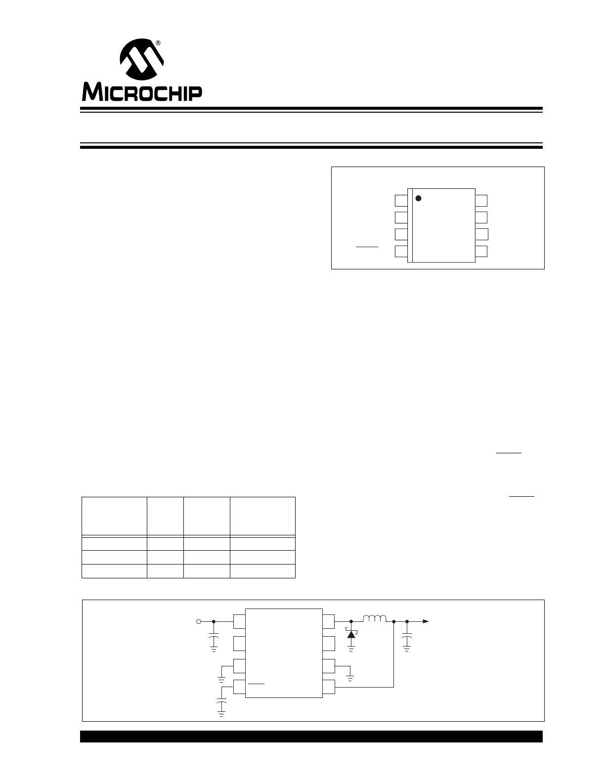
• Small 8-Pin SOP Package
Applications
• Portable Test Equipment
• Local Logic Supplies
• Portable Audio Systems
• Portable Scanners
• Palmtops
• Electronic Organizers
Device Selection Table
Package Type
General Description
TC120 is a 300kHz PFM/PWM step-down (Buck) DC/
DC regulator/controller combination for use in systems
operating from two or more cells, or in line-powered
applications. It uses PWM as the primary modulation
scheme, but automatically converts to PFM at low
output loads for greater efficiency. It requires only an
external inductor, Schottky diode, and two capacitors to
implement a step-down converter having a maximum
output current of 600mA (V
IN
= 5V, V
OUT
= 3.3V). An
external switching transistor (P-channel MOSFET) can
be added to increase output current capability to
support output loads of 2A or more.
The TC120 consumes only 55
A (max) of supply
current (V
OUT
= 3.3V) and can be placed in shutdown
mode by bringing the shutdown input (SHDN) low.
During shutdown, the regulator is disabled, supply
current is reduced to 2.5
A (max), and V
OUT
is
internally pulled to ground, discharging the output
capacitor. Normal operation resumes when SHDN is
brought high. Other features include a built-in under-
voltage lockout (UVLO), an externally programmable
soft start time, and output short circuit protection. The
TC120 operates from a maximum input voltage of 10V
and is available in a low-profile 8-Pin SOP package.
Functional Block Diagram
Part
Number
Output
Voltage
(V)
Package
Operating
Temp.
Range
TC120503EHA
5.0
8-Pin SOP -40°C to +85°C
TC120333EHA
3.3
8-Pin SOP -40°C to +85°C
TC120303EHA
3.0
8-Pin SOP -40°C to +85°C
1
2
3
4
8
7
6
5
TC120
8-Pin SOP
EXTW
CPC
SHDN/SS
V
IN
GND
EXT
SENSE
L
X
TC120XX03
V
IN
EXTW
CPC
SHDN/SS
L
X
EXT
GND
SENSE
C
IN
D1
L1
V
OUT
V
IN
C
OUT
C
SS
4.7nF
PWM/PFM Step-Down Combination Regulator/Controller
TC120
DS21365C-page 2
2001-2012 Microchip Technology Inc.
1.0
ELECTRICAL
CHARACTERISTICS
Absolute Maximum Ratings*
Power Supply Voltage (V
IN
).................... -0.3V to +12V
Voltage on V
OUT
Pin ............................... -0.3V to +12V
Voltage on LX, Boost Pins
................................... (V
IN
– 12V) to (V
IN
+ 0.3V)
Voltage on EXT1, EXT2, SHDN Pins
.......................................... (-0.3V) to (V
IN
+ 0.3V)
L
X
Pin Current .............................................. 700mA pk
EXT1, EXT2 Pin Current ...................................±50mA
Continuous Power Dissipation .........................300mW
Operating Temperature Range............. -40°C to +85°C
Storage Temperature Range ..............-40°C to +150°C
*Stresses above those listed under "Absolute Maximum
Ratings" may cause permanent damage to the device. These
are stress ratings only and functional operation of the device
at these or any other conditions above those indicated in the
operation sections of the specifications is not implied.
Exposure to Absolute Maximum Rating conditions for
extended periods may affect device reliability.
TC120 ELECTRICAL SPECIFICATIONS
Electrical Characteristics: Test circuit of Figure 3-1, T
A
= 25
C, V
IN
= V
R
x 1.2, Note 1 unless otherwise noted.
Symbol
Parameter
Min
Typ
Max
Units
Test Conditions
V
OUT
Output Voltage
V
R
x 0.975 V
R
± 0.5% V
R
x 1.025
V
V
OUT
= 3.0V
V
OUT
= 3.3V
V
OUT
= 5.0V
I
OUT
= 120mA (Note 1)
I
OUT
= 132mA
I
OUT
= 200mA
V
IN
Input Voltage
1.8
—
10.0
V
I
OUT
MAX
Maximum Output Current
500
600
600
—
—
—
—
—
—
mA
V
OUT
= 3.0V
V
OUT
= 3.3V
V
OUT
= 5.0V
I
IN
Supply Current
—
52
55
71
82
86
110
A
V
OUT
= 3.0V
V
OUT
= 3.3V
V
OUT
= 5.0V
V
IN
= V
R
x 1.05, no load
I
SHDN
Shutdown Supply Current
—
1.5
2.5
A
No load, SHDN = 0V, (Note 2)
I
LX
LX Pin Leakage Current
—
—
—
1.5
2
2.5
A
Measured at EXT1 Pin (Note 2)
No load, SHDN = 0V
R
DSON
(
L
X
)
LX Pin ON Resistance
—
—
—
0.69
0.64
0.44
0.94
0.85
0.58
V
OUT
= 3.0V
V
OUT
= 3.3V
V
OUT
= 5.0V
V
OUT
= V
R
x 0.9 (Note 2)
V
LX
= V
IN
– 0.2V, 10
Resistor from L
X
to V
IN
,
SHDN = V
IN
R
EXTH
EXT1, EXT2
On Resistance to V
IN
—
—
—
38
35
24
52
47
32
V
OUT
= 3.0V
V
OUT
= 3.3V
V
OUT
= 5.0V
SHDN = V
IH
; EXT1 and EXT2
connected to 200
load,
V
EXT1
= V
EXT2
= (V
IN
– 0.4V);
V
OUT
= V
IN
(Note 2)
R
EXTL
EXT1, EXT2
On Resistance to GND
—
—
—
31
29
20
41
37
26
V
OUT
= 3.0V
V
OUT
= 3.3V
V
OUT
= 5.0V
SHDN = V
IH
; EXT1 and EXT2
pulled up through a series
resistance of 200
to a voltage
such that VEXT1, 2 = 0.4V
f
OSC
Oscillator Frequency
255
300
345
kHz
Measured at EXT1 Pin,
V
IN
= V
OUT
+ 0.3V,
I
OUT
= 20mA (Note 3)
D
PWM
Maximum PWM Duty Cycle
—
—
100
%
D
PFM
PFM Duty Cycle
15
25
35
%
No load
Efficiency
—
95
—
%
V
IN
> V
R
x 1.2
Note
1:
V
R
is the factory-programmed output voltage setting.
2:
No external components connected, except C
SS.
3:
While operating in PWM Mode.
2001-2012 Microchip Technology Inc.
DS21365C-page 3
TC120
Electrical Characteristics: Test circuit of Figure 3-1, T
A
= 25
C, V
IN
= V
R
x 1.2, Note 1 unless otherwise noted.
Symbol
Parameter
Min
Typ
Max
Units
Test Conditions
V
UVLO
Minimum Operating Voltage
0.9
—
1.8
V
V
OUT
= V
R
x 0.9 (Note 2),
SHDN = V
IN
Measured with internal transistor
in OFF state and V
IN
falling
V
IH
SHDN Input Logic High,
Threshold Voltage
0.65
—
—
V
V
OUT
= 0V, (Note 2)
V
IL
SHDN Input Logic Low,
Threshold Voltage
—
—
0.20
V
V
OUT
= 0V, (Note 2)
t
PRO
Short Circuit Protection
Response Time
3
5
8
msec
Time from V
OUT
= 0V to
SHDN = V
IL
(Note 2)
t
SS
Soft Start Time
6
10
16
msec
Note
1:
V
R
is the factory-programmed output voltage setting.
2:
No external components connected, except C
SS.
3:
While operating in PWM Mode.

TC120
DS21365C-page 4
2001-2012 Microchip Technology Inc.
2.0
PIN DESCRIPTIONS
The descriptions of the pins are listed in Table 2-1.
TABLE 2-1:
PIN FUNCTION TABLE
Pin No.
(8-Pin SOP)
Symbol
Description
1
V
IN
Unregulated supply input.
2
EXTW
Extended external switching transistor drive output. This output follows the timing on the EXT
output with an additional 100nsec blanking time on both the leading and trailing edges. That is,
this output transitions from high-to-low 100 nsec prior to the same transition on EXT; and
transitions low-to-high 100nsec after the same transition on EXT; resulting in a longer external
switch ON time. (See Section 3.9 External Switching Transistor Selection).
3
CPC
Charge pump capacitor input. An inverting charge pump is formed by attaching a capacitor and
diode to this input. (See Section 3.5 Improving High Load Efficiency In Regulator Operating
Mode).
4
SHDN/SS
Shutdown and soft-start control input. A soft start capacitor of 100pF (min) must be connected to
this input. The soft start capacitor is charged by an internal
A current source that gently ramps
the TC120 into service. Shutdown control is best implemented with an external open collector (or
open drain) switch. The TC120 enters shutdown when this input is low. During shutdown, the
regulator is disabled, and supply current is reduced to less than 2.5
A. Normal operation is
restored when this input is open-circuited, and allowed to float high. (See Section 3.6 Low Power
Shutdown Mode/Soft Start Input).
5
SENSE
Voltage sense input. This input must be connected to the output voltage node at the physical
location that requires the tightest voltage regulation.
6
GND
Ground terminal.
7
EXT
External switching transistor drive output. This output connects directly to the gate of an external
P-channel MOSFET for applications requiring output currents greater than 600mA. The timing of
this output exactly matches that of the gate drive for the internal P-channel transistor. This output
can drive a maximum capacitance of 1000pF. (See Section 3.9 External Switching Transistor
Selection).
8
Lx
Inductor terminal. This pin is connected to the drain of the internal P-channel switching transistor.
If the TC120 is operated as a regulator (i.e., using the internal switch); the inductor must be
connected between this pin and the SENSE pin.
2001-2012 Microchip Technology Inc.
DS21365C-page 5
TC120
3.0
DETAILED DESCRIPTION
The TC120 can be operated as an integrated step-
down regulator (using the internal switching transistor);
or as a step-down regulator controller (using an
external switching transistor). When operating as an
integrated regulator, the only required external compo-
nents are a Schottky diode, inductor and an output
capacitor. Operating in this configuration, the TC120 is
capable of supporting output load currents to a
maximum of 600mA with operating efficiencies above
85%. Efficiencies at high loads can be further improved
by using the on-board charge pump circuit to pull the
gate of the internal switching transistor below ground
for the lowest possible ON resistance. (For more infor-
mation, see Section 3.5 Improving High Load
Efficiency in Regulator Operating Mode).
Higher output currents are achieved by operating the
TC120 with an external P-channel switching transistor
(controller mode). In this operating configuration, the
maximum output current is determined primarily by the
ON resistance of the P-channel switch and the series
resistance of the inductor.
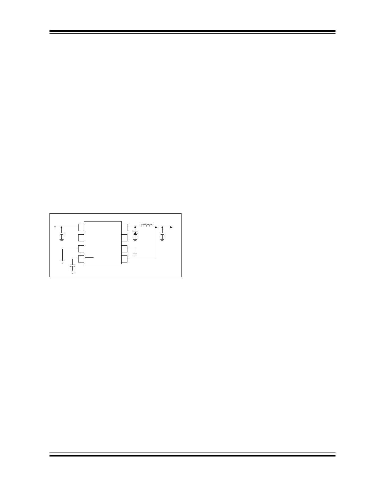
FIGURE 3-1:
TEST CIRCUIT
3.1
Inductor Selection
Selecting the proper inductor value is a trade-off
between physical size and power conversion require-
ments. Lower value inductors cost less, but result in
higher ripple current and core losses. They are also
more prone to saturate since the coil current ramps
faster and could overshoot the desired peak value. This
not only reduces efficiency, but could also cause the
current rating of the external components to be
exceeded. Larger inductor values reduce both ripple
current and core losses, but are larger in physical size
and tend to increase the start-up time slightly. A 22
H
inductor is the best overall compromise and is recom-
mended for use with the TC120. For highest efficiency,
use inductors with a low DC resistance (less than
20m
). To minimize radiated noise, consider using a
toroid, pot core or shielded-bobbin inductor.
3.2
Input Bypass Capacitor
Using an input bypass capacitor reduces peak current
transients drawn from the input supply, and reduces the
switching noise generated by the regulator. The source
impedance of the input supply determines the size of
the capacitor that should be used.
3.3
Output Capacitor
The effective series resistance of the output capacitor
directly affects the amplitude of the output voltage
ripple. (The product of the peak inductor current and
the ESR determines output ripple amplitude.) There-
fore, a capacitor with the lowest possible ESR should
be selected. Smaller capacitors are acceptable for light
loads or in applications where ripple is not a concern. A
47
F Tantalum capacitor is recommended for most
applications. The Sprague 595D series of tantalum
capacitors are amongst the smallest of all low ESR
surface mount capacitors available. Table 3-1 lists
suggested components and suppliers.
3.4
Catch Diode
The high operating frequency of the TC120 requires a
high-speed diode. Schottky diodes such as the MA737
or 1N5817 through 1N5823 (and the equivalent surface
mount versions) are recommended. Select a diode
whose average current rating is greater than the peak
inductor current; and whose voltage rating is higher
than V
IN
MAX
.
3.5
Improving High Load Efficiency in
Regulator Operating Mode
If the TC120 is operated at high output loads most (or
all) of the time, efficiency can be improved with the
addition of two components. Ordinarily, the voltage
swing on the gate of the internal P-channel transistor is
from ground to V
IN
. By adding a capacitor and diode as
shown in Figure 3-2, an inverting charge pump is
formed, enabling the internal gate voltage to swing
from a negative voltage to +V
IN
. This increased drive
lowers the R
DS
ON
of the internal transistor, improving
efficiency at high output currents. Care must be taken
to ensure the voltage measured between V
IN
and CPC
does not exceed an absolute value of 10V. While this is
not a problem at values of V
IN
at (or below) 5V, higher
V
IN
values will require the addition of a clamping
mechanism (such as a Zener diode) to limit the voltage
as described. While this technique improves efficiency
at high output loads, it is at the expense of low load
efficiency because energy is expended charging and
discharging the charge pump capacitor. This technique
is therefore not recommended for applications that
operate the TC120 at low output currents for extended
time periods. If unused, CPC must be grounded.
TC120XX03
V
IN
EXTW
CPC
SHDN/SS
L
X
EXT
GND
SENSE
47
μF/10V
Tantalum
C
SS
4.7nF
IN5817
L1
22
μH
V
OUT
V
IN
C
OUT
47
μF/10V
Tantalum
+
–
+
–

TC120
DS21365C-page 6
2001-2012 Microchip Technology Inc.
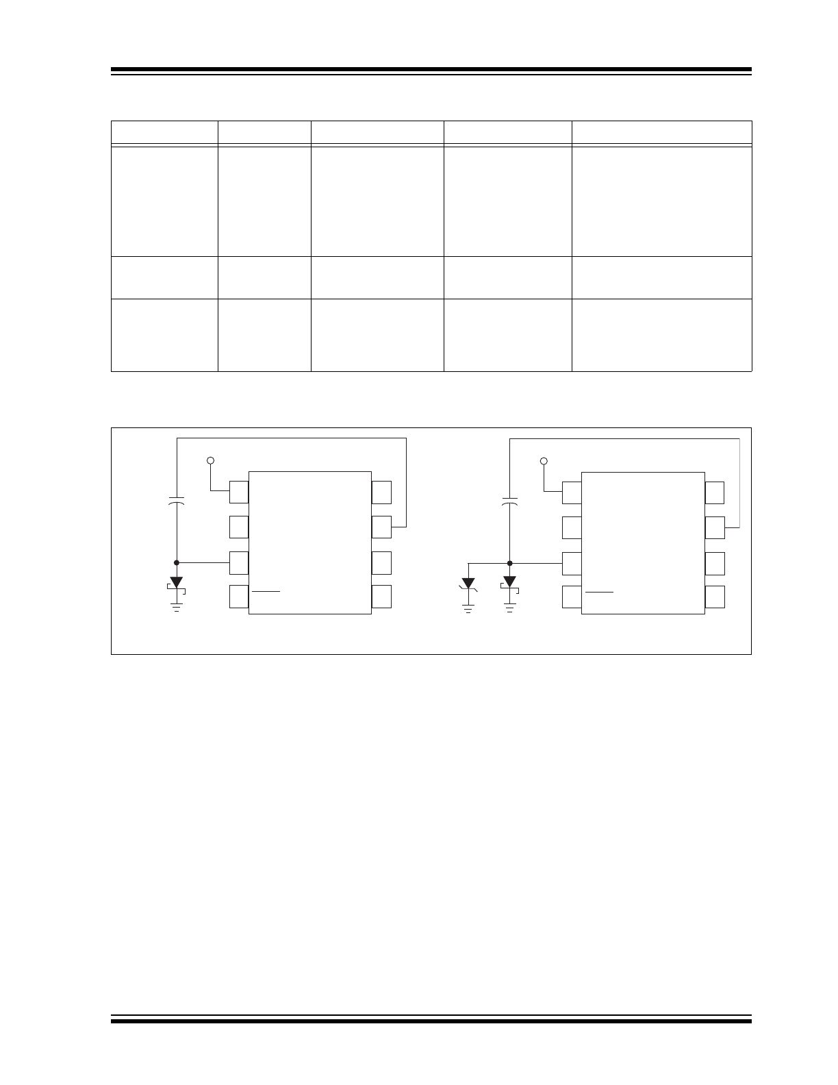
3.6
Low Power Shutdown Mode/Soft
Start Input
The SHDN/SS input acts as both the shutdown control
and the node for the external soft start capacitor, which
is charged by an internal 1
A current source. A value
of 4700pF (100pF minimum) is recommended for the
soft start capacitor. Failure to do this may cause large
overshoot voltages and/or large inrush currents result-
ing in possible instability. The TC120 enters a low
power shutdown mode when SHDN/SS is brought low.
While in shutdown, the oscillator is disabled and the
output discharge switch is turned on, discharging the
output capacitor. Figure 3-3 shows the recommended
interface circuits to the SHDN/SS input. As shown, the
SHDN/SS input should be controlled using an open
collector (or open drain) device, such that the SHDN/
SS input is grounded for shutdown mode, and open-
circuited for normal operation (Figure 3-3a). If a CMOS
device is used to control shutdown (Figure 3-3b), the
value of R1 and C
SS
should be chosen such that the
voltage on SHDN/SS rises from ground to 0.65V in
1.5msec (Figure 3-4). If shutdown is not used, C
SS
must still be connected as shown in Figure 3-3c and
Figure 3-3d. SHDN/SS may be pulled up with a resistor
(Figure 3-3c) as long as the values of R
SS
and C
SS
provide the approximate charging characteristic on
power up shown in Figure 3-4. C
SS
only may also be
connected as shown in Figure 3-3d with C
SS
chosen at
4700pF (minimum 100pF).
3.7
Undervoltage Lockout (UVLO)
The TC120 is disabled whenever V
IN
is below the
undervoltage lockout threshold. This threshold is equal
to the guaranteed minimum operating voltage for the
TC120 (i.e., 2.2V). When UVLO is active, the TC120 is
completely disabled.
3.8
Short Circuit Protection
Upon detection of an output short circuit condition, the
TC120 reduces the PWM duty cycle to a minimum
value using its internal protection timer. The sequence
of events is as follows: when an output voltage
decrease to near zero is detected (as the result of an
overload), the internal (5msec) protection timer is
started. If the output voltage has not recovered to
nominal value prior to the expiration of the protection
timer, the TC120 is momentarily shut down by
dedicated, internal circuitry. Immediately following this
action, the soft start sequence is engaged in an attempt
to re-start the TC120. If the output short circuit is
removed, normal operation is automatically restored. If
the short circuit is still present, the timed self-shutdown
sequence described above is repeated.
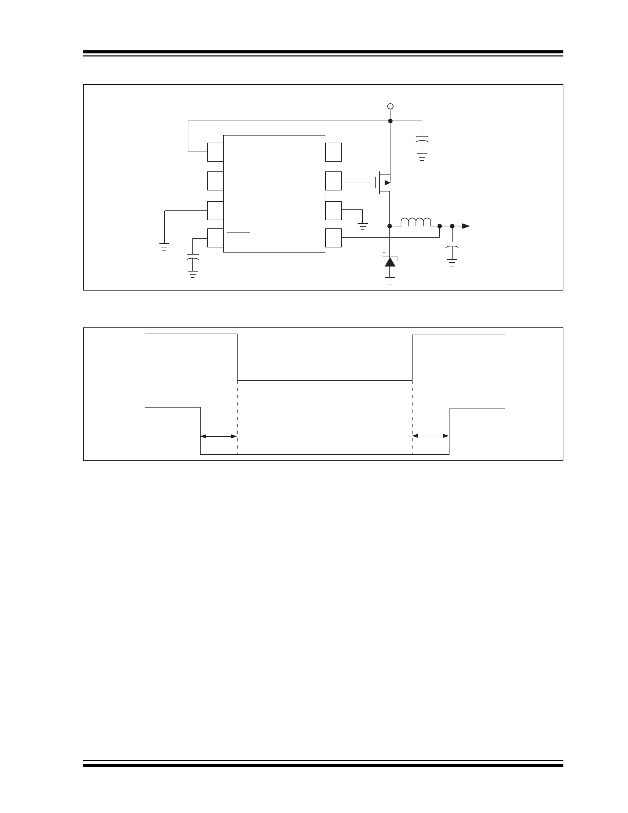
3.9
External Switching Transistor
Selection
EXT is a complimentary output with a maximum ON
resistances of 32
to V
DD
when high and 26
to
ground when low, at V
OUT
= 5V. It is designed to
directly drive a P-channel MOSFET (Figure 3-5). The
P-channel MOSFET selection is determined mainly by
the on-resistance, gate-source threshold and gate
charge requirements. Also, the drain-to-source and
gate-to-source breakdown voltage ratings must be
greater than V
IN
MAX
. The total gate charge specification
should be less than 100nC for best efficiency. The
MOSFET must be capable of handling the required
peak inductor current, and should have a very low on-
resistance at that current. For example, a Si9430
MOSFET has a drain-to-source rating of -20V, and a
typical on-resistance r
DS
ON
of 0.07
at 2A, with V
GS
=
-4.5V. (EXTW (Figure 3-6) may be gated with external
circuitry to add blanking, or as an auxiliary timing
signal.) Table 3-1 lists suggested components and
suppliers.
3.10
Board Layout Guidelines
As with all inductive switching regulators, the TC120
generates fast switching waveforms, which radiate
noise. Interconnecting lead lengths should be
minimized to keep stray capacitance, trace resistance
and radiated noise as low as possible. In addition, the
GND pin, input bypass capacitor and output filter
capacitor ground leads should be connected to a single
point. The input capacitor should be placed as close to
power and ground pins of the TC120 as possible. The
length of the EXT trace must also be kept as short as
possible.
2001-2012 Microchip Technology Inc.
DS21365C-page 7
TC120
TABLE 3-1:
SUGGESTED COMPONENTS AND SUPPLIERS
FIGURE 3-2:
TC120 WITH ADDED COMPONENTS FOR IMPROVED EFFICIENCY AT
HIGH OUTPUT CURRENTS
Type
Inductors
Capacitors
Diodes
Transistors
Surface Mount
Sumida
CD54 Series
CDRH Series
Coilcraft
DO Series
AVX
TPS Series
Sprague
595D Series
ON Semiconductor
MBRS340T3
Nihon
NSQ Series
Matsushita
MA737
Silconix
Little Foot MOSFET Series
Zetex FZT749
PNP Bipolar Transistor
Toshiba 2SA1213 PNP
Transistor
Miniature
Through-Hole
Sumida
RCH Series
Sanyo
OS-CON Series
IRC
OAR Series
Standard
Through-Hole
Coilcraft
PCH Series
Nichicon
PL Series
United Chemi-Conv
LXF Series
ON Semiconductor
TMOS Power MOSFETs
TC120XX03
V
IN
EXTW
CPC
SHDN/SS
L
X
EXT
GND
SENSE
D
1
IN5817
a) For V
IN
≤ 5V
C
P
2200 pF
Ceramic
TC120XX03
V
IN
EXTW
CPC
SHDN/SS
L
X
EXT
GND
SENSE
D
1
IN5817
b) For V
IN
> 5V
C
P
2200 pF
Ceramic
10V
Zener
Diode
V
IN
≤ 5V
V
IN
> 5V
TC120
DS21365C-page 8
2001-2012 Microchip Technology Inc.
FIGURE 3-3:
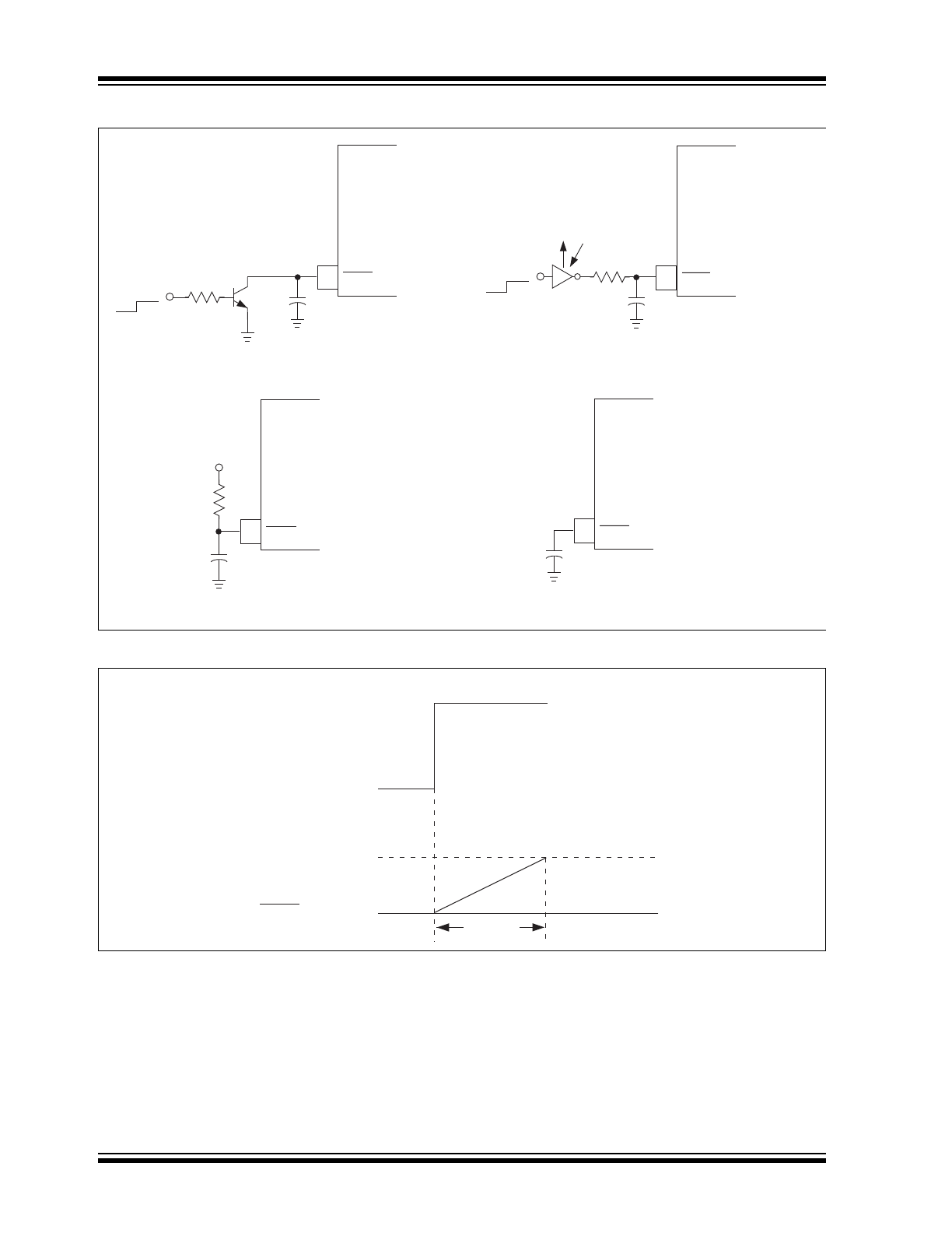
SHUTDOWN CONTROL CIRCUITS
FIGURE 3-4:
SOFT START TIMING
SHDN/SS
TC120XX03
C
SS
SHDN/SS
TC120XX03
C
SS
SHDN/SS
TC120XX03
C
SS
4.7nF
SHDN/SS
TC120XX03
R
SS
V
IN
SHDN
ON OFF
47K
2N2222
C
SS
4.7nF
R
1
V
IN
CMOS
Gate
a) Using an Open Collector Device
b) Using a Complementary Output Device
c) Shutdown Not Used – with Pull-Up
d) Shutdown Not Used – No Pull-Up
SHDN
ON OFF
OFF
ON
0.65V
0V
1.5msec
SHDN/SS
Shutdown
Signal
X
2001-2012 Microchip Technology Inc.
DS21365C-page 9
TC120
FIGURE 3-5:
USING EXTERNAL TRANSISTOR SWITCH
FIGURE 3-6:
EXTERNAL (EXT) AND EXTENDED EXTERNAL (EXTW) SWITCHING
TRANSISTOR DRIVE OUTPUT
TC120XX03
V
IN
EXTW
CPC
L
X
EXT
GND
SENSE
SHDN/SS
C
SS
4.7 nF
IN5817
L1
22
μH
V
OUT
V
IN
C
IN
47
μF
Tantalum
C
OUT
47
μF
Tantalum
EXT
EXTW
100nsec
100nsec
TC120
DS21365C-page 10
2001-2012 Microchip Technology Inc.
4.0
PACKAGING INFORMATION
4.1
Package Marking Information
Package marking data not available at this time.
4.2
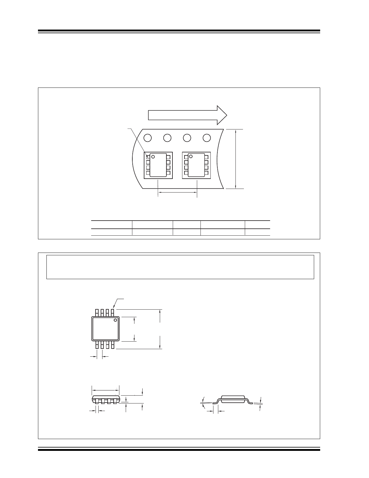
Taping Form
4.3
Package Dimensions
Component Taping Orientation for 8-Pin SOP Devices
Package
Carrier Width (W)
Pitch (P)
Part Per Full Reel
Reel Size
8-Pin SOP
12 mm
8 mm
1000
7 in
Carrier Tape, Number of Components Per Reel and Reel Size
PIN 1
User Direction of Feed
Standard Reel Component Orientation
for TR Suffix Device
W
P
8-Pin SOP
.181 (4.60)
.165 (4.20)
.217 (5.50)
.193 (4.90)
.069 (1.75)
.055 (1.40)
.008 (0.20)
.000 (0.00)
.020 (0.50)
.012 (0.30)
.256 (6.50)
.232 (5.90)
PIN 1
.010 (0.25)
.004 (0.10)
.018 (0.45)
.014 (0.35)
8
° MAX.
.051 (1.30)
.049 (1.24)
Dimensions: inches (mm)
Note:
For the most current package drawings, please see the Microchip Packaging Specification located
at http://www.microchip.com/packaging