
2002-2012 Microchip Technology Inc.
DS21364C-page 1
TC1188/TC1189
Features
• Input Voltage Range: 2.7 V to 6.0 V
• 120 mA Output Current
• Low Supply Current: 50 µA, (typical)
• Low Dropout Voltage: 110 mV, (typical at 100 mA)
• Fast Turn-On from Shutdown: 140 µsec (typical)
• Low Output Noise
• Over-Current and Over-Temperature Protection
• Low Power Shutdown Mode
• Auto Discharge of Output Capacitor (TC1189)
Applications
• Battery Powered Systems
• Portable Computers
• Medical Instruments
• Cellular, Cordless Phones
• PDAs
• Pagers
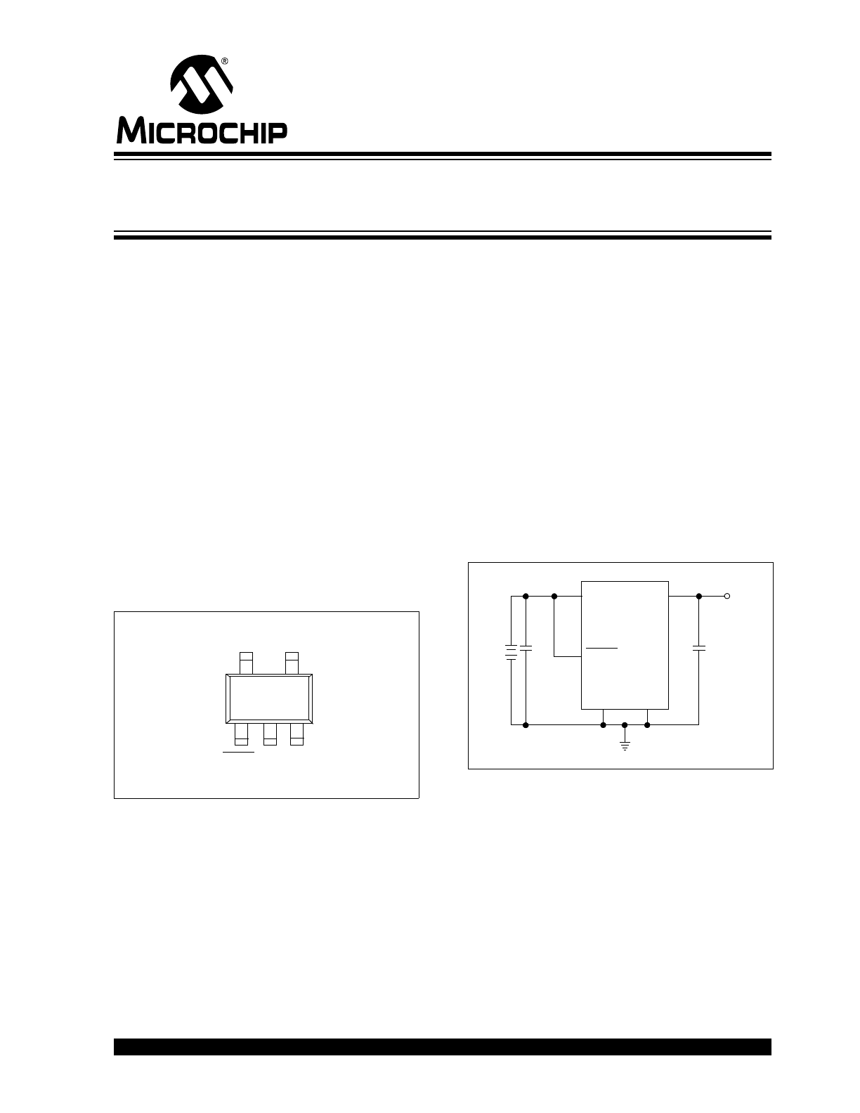
Package Type
General Description
The TC1188 and TC1189 are fixed output, low dropout
linear regulators that operate from a 2.7V to 6.0V input
voltage source. The output is capable of delivering up
to 120 mA while consuming only 50 µA of quiescent
current. The low dropout voltage, 120 mV, make the
TC1188 and TC1189 good choices for battery powered
applications. Integrated over-current and over-temper-
ature protection features provide for a fault tolerant
solution.
The TC1189 includes an output voltage auto discharge
feature. When shutdown, the TC1189 will automatically
discharge the output voltage using an internal N-Chan-
nel MOSFET switch.
Fixed output voltage options for the TC1188/TC1189
are: 1.80V, 2.80V, 2.84V and 3.15V. Both the TC1188
and TC1189 are available in SOT23-5 packages.
Typical Application Circuit
GND
SHDN GND
5
1
4
2
3
TC1188
TC1189
5-Pin SOT-23A
NOTE:
5-Pin SOT-23A is equivalent to the EIAJ (SC-74A)
V
IN
V
OUT
V
OUT
V
IN
Output
GND
SHDN
TC1188
TC1189
+
1 µF
–
C
OUT
GND
Voltage
1 µF
C
IN
Battery
MAX8863/64 Pin Compatible, Low Dropout,
120 mA Linear Regulators
TC1188/TC1189
DS21364C-page 2
2002-2012 Microchip Technology Inc.
1.0
ELECTRICAL
CHARACTERISTICS
Absolute Maximum Ratings*
Input Voltage .........................................................6.5V
Output Short-Circuit Duration.............................Infinite
Output Voltage........................... (-0.3V) to (V
IN
+ 0.3V)
Maximum Voltage On Any Pin.... (-0.3V) to (V
IN
+0.3V)
Continuous Power Dissipation (T
A
= +70°C)
SOT-23-5 (derate 7.1 mW/°C above +70°C)
..................................................................571 mW
Operating Temperature Range...............-40°C to 85°C
Storage Temperature..........................-65°C to +160°C
Lead Temperature (Soldering, 10 Sec.) ........... +300°C
*Notice: *Stresses above those listed under "Absolute
Maximum Ratings" may cause permanent damage to
the device. These are stress ratings only and functional
operation of the device at these or any other conditions
above those indicated in the operation sections of the
specifications is not implied. Exposure to Absolute
Maximum Rating conditions for extended periods may
affect device reliability.
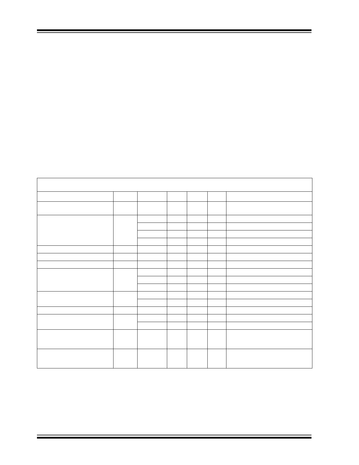
DC SPECIFICATIONS
Electrical Characteristics:
V
IN
= +3.6V, GND = 0V, T
A
= T
MIN
to T
MAX
, unless otherwise noted. Typical values are at T
A
= +25°C.
(Note 1)
Parameters
Symbol
Min
Typ
Max
Units
Conditions
Input Voltage
V
IN
V
OUT
+0.5V
2.7
—
—
6.0
6.0
V
V
OUT
2.5V
V
OUT
= 1.8V (Note 2)
Output Voltage
V
OUT
3.05
3.15
3.25
V
0 mA
I
OUT
50 mA
T
2.75
2.84
2.93
V
0 mA
I
OUT
50 mA
S
2.70
2.80
2.88
V
0 mA
I
OUT
50 mA
R
1.745
1.80
1.85
V
0 mA
I
OUT
50 mA
Q
Maximum Output Current
I
OUT
120
—
—
mA
Current Limit
I
LIM
—
280
—
mA
Note 3
Input Current
I
IN
—
50
90
µA
I
OUT
= 0
Dropout Voltage
—
1.1
—
mV
I
OUT
= 1 mA
—
55
120
mV
I
OUT
= 50 mA
—
110
240
mV
I
OUT
= 100 mA (Note 4)
Line Regulation
V
LNR
-0.10
0.001
0.10
%/V
V
IN
= V
OUT
0.5V to 6.0V
—
—
—
%/V
I
OUT
= 1 mA
Load Regulation
V
LDR
—
0.01
0.040
%/mA I
OUT
= 0 mA to 50 mA
Output Voltage Noise
—
350
—
µV
RMS
10 Hz to 1 MHz, C
OUT
= 1
Μ
F
—
220
—
µV
RMS
10 Hz to 1 MHz C
OUT
= 100
Μ
F
Wake Up Time
(from Shutdown Mode)
t
WK
—
10
—
µsec
V
IN
= 3.6V
C
IN
= 1 µF, C
OUT
= 1 µF
I
L
= 30 mA, (See Figure 3-1)
Setting Time
(from Shutdown Mode)
t
S
—
140
—
µsec
V
IN
= 3.6V
C
IN
= 1 µF, C
OUT
= 1 µF
I
L
= 30 mA, (See Figure 3-1)
Note
1:
Limits are 100% production tested at T
A
= +25°C. Limits over the operating temperature range are ensured through cor-
relation using Statistical Quality Control (SQC) methods.
2:
Validated by line regulation test.
3:
Not tested. For design purposes, the current limit should be considered 150 mA minimum to 410 mA maximum.
4:
The dropout voltage is defined as (V
IN
– V
OUT
) when V
OUT
is 100 mV below the value of V
OUT
for
V
IN
= V
OUT
+2V.
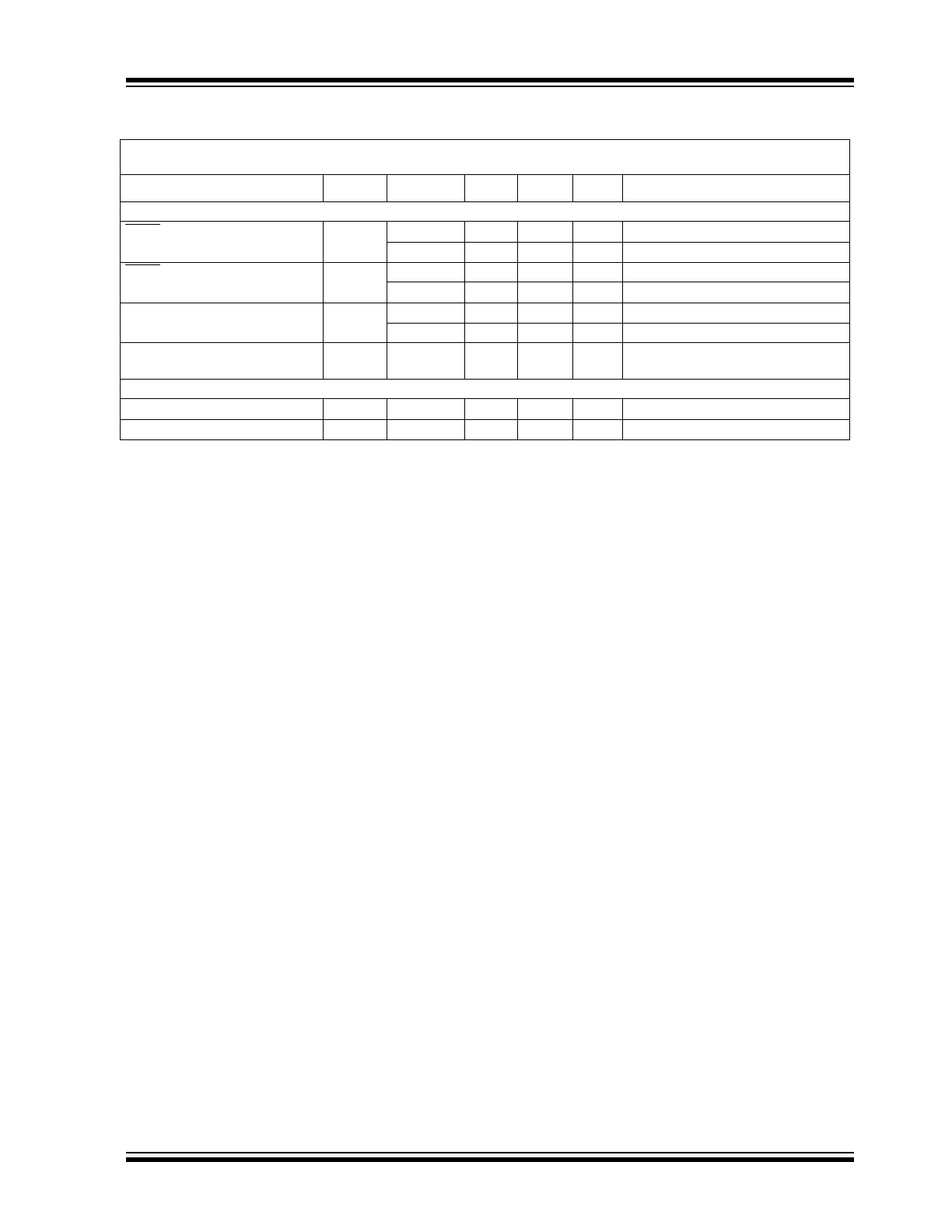
2002-2012 Microchip Technology Inc.
DS21364C-page 3
TC1188/TC1189
Shutdown:
SHDN Input Threshold
V
IH
2.0
—
—
V
V
IL
—
—
0.4
V
SHDN Input Bias Current
I
shdn
—
0.1
100
nA
V
SHDN
= V
IN
, T
A
= +25°C, T
A
= T
MAX
—
50
—
nA
V
SHDN
= V
IN
, T
A
= +25°C, T
A
= T
MAX
Shutdown Supply Current
I
qshdn
—
0.002
1
A
V
OUT
= 0V, T
A
= +25°C, T
A
= T
MAX
—
0.02
—
A
V
OUT
= 0V, T
A
= +25°C, T
A
= T
MAX
Shutdown to Output Discharge
Delay (TC1189)
—
1
—
msec
C
OUT
= 1
F, no load at 10% of V
OUT
Thermal Protection
Thermal Shutdown Temperature
T
SHDN
—
170
—
°C
Thermal Shutdown Hysteresis
T
SHDN
—
20
—
°C
DC SPECIFICATIONS (CONTINUED)
Electrical Characteristics:
V
IN
= +3.6V, GND = 0V, T
A
= T
MIN
to T
MAX
, unless otherwise noted. Typical values are at T
A
= +25°C.
(Note 1)
Parameters
Symbol
Min
Typ
Max
Units
Conditions
Note
1:
Limits are 100% production tested at T
A
= +25°C. Limits over the operating temperature range are ensured through cor-
relation using Statistical Quality Control (SQC) methods.
2:
Validated by line regulation test.
3:
Not tested. For design purposes, the current limit should be considered 150 mA minimum to 410 mA maximum.
4:
The dropout voltage is defined as (V
IN
– V
OUT
) when V
OUT
is 100 mV below the value of V
OUT
for
V
IN
= V
OUT
+2V.
TC1188/TC1189
DS21364C-page 4
2002-2012 Microchip Technology Inc.
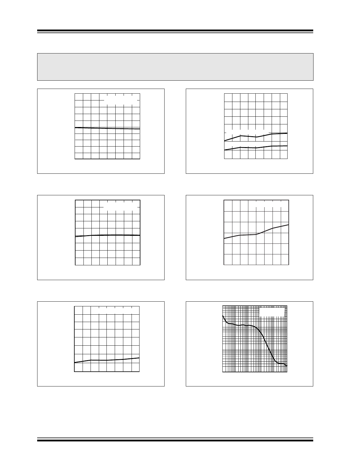
2.0
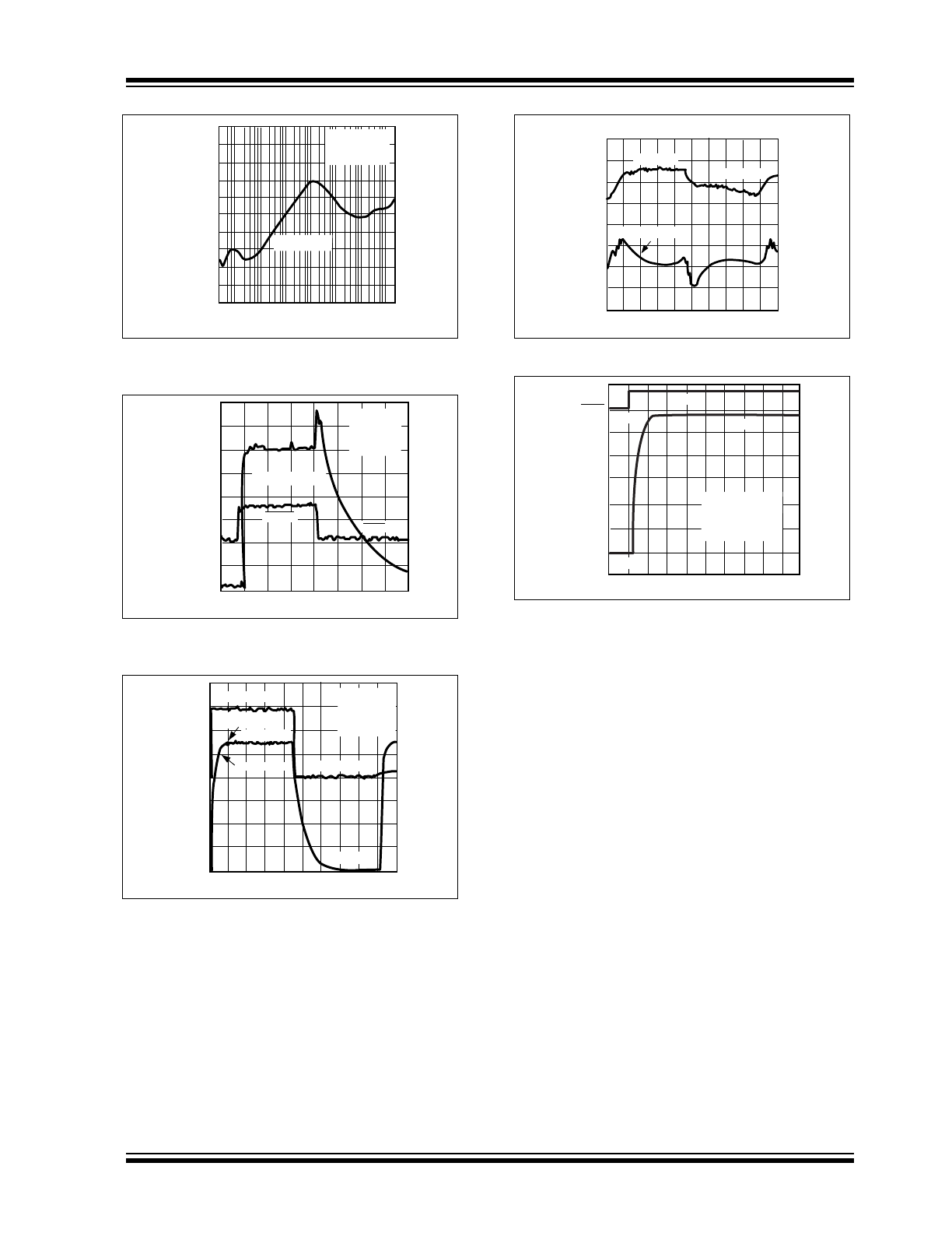
TYPICAL PERFORMANCE CURVES
FIGURE 2-1:
Line Regulation vs.
Temperature. (TC1188)
FIGURE 2-2:
Output Voltage vs.
Temperature. (TC1188)
FIGURE 2-3:
Load Regulation vs.
Temperature. (TC1188)
FIGURE 2-4:
Load Regulation vs.
Temperature. (TC1188)
FIGURE 2-5:
Dropout Voltage vs.
Temperature. (TC1188)
FIGURE 2-6:
Output Noise vs. Frequency.
(TC1188)
Note:
The graphs and tables provided following this note are a statistical summary based on a limited number of
samples and are provided for informational purposes only. The performance characteristics listed herein are
not tested or guaranteed. In some graphs or tables, the data presented may be outside the specified
operating range (e.g., outside specified power supply range) and therefore outside the warranted range.
0.10
0.08
0.06
0.04
0.00
–0.02
–0.04
–0.06
–0.08
–0.10
0.02
–40
°
C
0
°
C
25
°
C
70
°
C
85
°
C
TEMPERATURE (
°
C)
LINE REGULATION (%)
Line Reg. @ 3.50 V
to 5.50V(%)
2.930
2.910
2.890
2.870
2.850
2.830
2.810
2.790
2.770
2.750
–40
°
C
0
°
C
25
°
C
70
°
C
85
°
C
TEMPERATURE (
°
C)
V
OUT
(V)
V
OUT
- SET/1.0mA
@ 3.5V (V)
0.040
0.035
0.030
0.025
0.020
0.015
0.010
0.005
0.000
–40
°
C
0
°
C
25
°
C
70
°
C
85
°
C
TEMPERATURE (
°
C)
LOAD REGULATION (%)
Load Reg. 0 to 50mA (%)
0.040
0.035
0.030
0.025
0.020
0.015
0.010
0.005
0.000
–40
°
C
0
°
C
25
°
C
70
°
C
85
°
C
TEMPERATURE (
°
C)
LOAD REGULATION (%)
Load Reg. 0 to 50mA (%)
Load Reg. 0 to 100mA (%)
0.120
0.100
0.080
0.060
0.040
0.020
0.000
–40
°
C
0
°
C
25
°
C
70
°
C
85
°
C
TEMPERATURE (
°
C)
(V)
50mA, Dropout V (V)
FREQUENCY (kHz)
Noise (
μ
V/
√
HZ)
10.0
1.0
0.01
0.01
1
10
100
1000
0.1
0.0
R
LOAD
= 50μΩ
C
OUT
= 1
μF
2002-2012 Microchip Technology Inc.
DS21364C-page 5
TC1188/TC1189
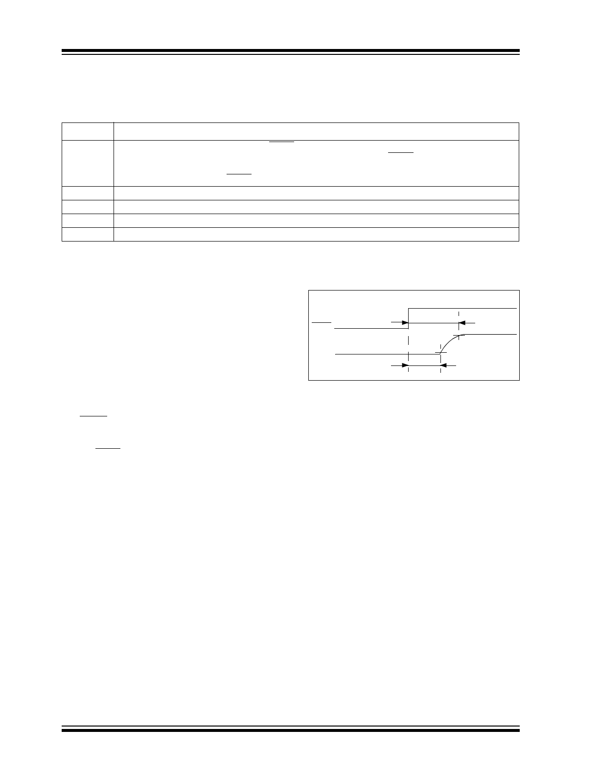
FIGURE 2-7:
Power Supply Rejection
Ratio vs. Frequency. (TC1188)
FIGURE 2-8:
TC1189 Shutdown Transient
Response.
FIGURE 2-9:
TC1189 Shutdown Transient
Response.
FIGURE 2-10:
TC1189 Line Response.
FIGURE 2-11:
Wake-Up Response Time.
FREQUENCY (kHz)
(dB)
10
100 1K
10K
1M
10M
100K
C
OUT
= 1
μF
-10
-20
-30
-40
-60
-70
-50
-80
-90
-100
V
OUT
= 2.84V
R
LOAD
= 50Ω
100mV p-p
CH2 GND
CH1 GND
200
μsec/Div
SHDN
SHDN = 0V
V
OUT
= 0.5V/DIV
T = 25
°
C
IN
= 1
μF
C
L
=1
μF
R
L
=
∞
CH2 GND
CH1 GND
CH1
CH2
200
μsec/Div
C
IN
= 1
μF
C
OUT
=1
μF
R
L
=
100Ω
V
IN
= 3.5V
T
T
XSHDN = 3V
Turn On
Time = 150
μS
No Overshoot
V
OUT
= 2.7V
XSHDN = 0V
V
OUT
= 0V
CH2 GND
CH2
CH1 GND
CH1
100
μsec/Div
C
IN
= C
OUT
= 1
μF, R
L
= 470
Ω, XSHDN = 3.5V
T
T
V
OUT
AC
20
μV/DIV
V
IN
= 4.5V
V
IN
= 3.5V
TIME (100
μs/Div)
OUTPUT, SHUTDOWN VOLTAGE (V)
SHDN
VOUT
0V
2.8V
0V
3V
V
IN
= 3.6V
I
LOAD
= 30mA
C
IN
=
1
μF
C
LOAD
= 1
μF
TC1188/TC1189
DS21364C-page 6
2002-2012 Microchip Technology Inc.
3.0
PIN DESCRIPTIONS
The descriptions of the pins are listed in Table 3-1.
TABLE 3-1:
PIN FUNCTION TABLE
3.1
Detailed Description
The TC1188/TC1189 devices are fixed output, low
dropout linear regulators. Utilizing CMOS construction,
the internal quiescent current consumed by the regula-
tor is minimized when compared to older bipolar low
dropout regulators.
The LDO output voltage is sensed at the non-inverting
pin of the internal error amplifier. The internal voltage
reference is sensed at the inverting pin of the internal
error amplifier. The error amplifier adjusts the gate
source voltage of the internal P-channel pass device
until the divided down output voltage matches the inter-
nal reference voltage. When it does, the LDO output
voltage is in regulation.
The SHDN, when pulled low, is used to turn off the P-
Channel MOSFET and lower the internal quiescent
current to less than 1 µA maximum. For normal opera-
tion, the SHDN pin is pulled to a high level. (> 2.0V).
The TC1189 incorporates an internal N-Channel MOS-
FET, which is used to discharge the output capacitor
when shutdown. The TC1188 does not have the inter-
nal N-Channel MOSFET, therefore, when the device is
shutdown, the output voltage will decrease at a rate
which is dependant on the load current.
3.2
Turn-On Response
The turn-on response is defined as two separate
response categories: Wake-Up Time (t
WK
) and Settling
Time (t
S
).
The TC1188/TC1189 have fast wake-up times (10 µsec
typical) when released from shutdown. See Figure 3-1
for the wake-up time, designated as t
WK
. The wake-up
time is defined as the time it takes for the output to rise
to 2% of the V
OUT
value after being released from shut-
down.
The total turn on response is defined as the Settling
Time (t
S
) (Figure 3-1). Settling Time (inclusive with t
WK
)
is defined as the condition when the output is within 2%
of its fully enabled value (140 µsec typical) when
released from shutdown. The settling time of the output
voltage is dependent on load conditions and output
capacitance on V
OUT
(RC response).
FIGURE 3-1:
Wake-Up Response Time.
3.3
Internal P-Channel Pass
Transistor
The Internal P-Channel MOSFET is operated in the lin-
ear region to regulate the LDO output voltage. The
RDSon of the P-Channel MOSFET is approximately
1.1
making the LDO able to regulate with little input
to output voltage differential, "Low Dropout". Another
benefit of using CMOS construction is that the P-Chan-
nel MOSFET is a voltage controlled device, so it
doesn't consume a fraction of the bias current required
of bipolar PNP LDOs.
Symbol
Description
SHDN
Active Low Shutdown Input. When the SHDN input is low (< 0.2V), the quiscent current for the
TC1188/TC1189 is reduced to 0.1 nA. When the input voltage to the SHDN pin is high (> 2.0V) the
output of the TC1188/TC1189 is enabled. For the TC1189 only, the output capacitor is discharged by
an internal switch when the SHDN is low.
GND
Ground. Connect to ground.
V
IN
Unregulated Input Voltage. The input voltage can range from 2.7V to 6.0V.
V
OUT
Regulator Output. Sources up to 120 mA. Bypass with a 1 µF, <1
typical ESR capacitor to GND.
GND
Connect to GND.
V
IH
t
S
t
WK
V
OUT
98%
2%
V
IL
SHDN
2002-2012 Microchip Technology Inc.
DS21364C-page 7
TC1188/TC1189
FIGURE 3-2:
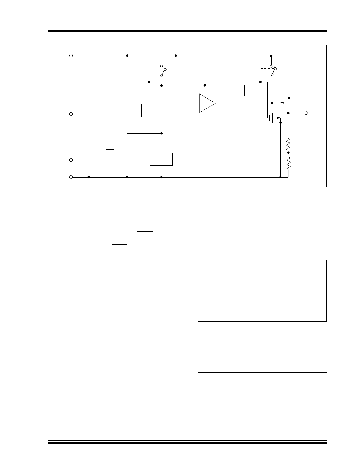
Functional Block Diagram.
3.4
Shutdown
The SHDN input is used to turn off the LDO P-Channel
pass MOSFET and internal bias. When shutdown, the
typical quiescent current consumed by the LDO is
0.1 nA. A logic low (< 0.4V) at the SHDN input will
cause the device to operate in the shutdown mode. A
logic high (> 2.0V) at the SHDN input will cause the
device to operate in the normal mode.
3.5
Current Limit
The LDO output current is monitored internal to the
TC1188/TC1189. The internal current sense will limit
the LDO output current to a typical value of 280 mA.
The current limit can range from approximately 50 mA
to 410 mA from device to device. The internal current
limit protects the device from a continuous output short
circuit.
3.6
Thermal Overload Protection
Integrated thermal protection circuitry shuts the
TC1188/TC1189 off when the internal die temperature
exceeds approximately 170°C. The regulator output
remains off until the internal die temperature drops to
approximately 150°C.
3.7
Operating Region and Power
Dissipation
The internal power dissipation to the LDO is primarily
determined by the input voltage, output voltage and
output current. The following equation is used to
approximate the worst case for power dissipation:
EQUATION
The maximum power dissipation is a function of the
maximum ambient temperature, T
A(MAX)
, the maximum
junction temperature, T
J(MAX)
, and the package thermal
resistance from junction to air,
JA
. The 5-Pin SOT23A
package has a
JA
of approximately 220°C/Watt.
EQUATION
Bandgap
Reference
MOS Driver
W
ith
I
LIMIT
Thermal
Sensor
Shutdown
Logic
Error
+
–
V
IN
SHDN
GND
V
OUT
PMOS Pass
GND
N
(TC1189 Only)
Amplifier
Transistor
P
D
= V
IN(MAX)
- V
OUT(MIN)
x I
LOAD(MAX)
Where:
P
D
= Worst case internal power dissipation.
V
IN
(
MAX
)
= Maximum input voltage.
V
OUT
(
MIN
)
= Minimum output voltage.
I
LOAD
(
MAX
)
= Maximum output current.
P
D
= (T
J(MAX)
- T
A(MAX)
)/
JA
Where all terms are previously defined.
TC1188/TC1189
DS21364C-page 8
2002-2012 Microchip Technology Inc.
EXAMPLE 3-1:
The previously defined power dissipation equations
can be used to ensure that the regulator thermal
operation is within limits.
Given:
V
IN(MAX)
= 3.0V +10%
V
OUT(MAX)
= 2.7V - 2.5%
I
LOAD(MAX)
= 40
M
A
T
J(MAX)
= 125°C
T
A(MAX)
= 55°C
Find:
1.
Actual power dissipation.
2.
Maximum allowable dissipation.
Actual power dissipation:
Maximum allowable power dissipation:
In this example, the TC1188/TC1189 dissipates a max-
imum of 26.7 mW below the allowable limit of 318 mW.
In a similar manner, the power dissipation equation, as
a function of V
IN
, V
OUT
and I
LOAD,
along with the power
dissipation equation, as a function of maximum junction
temperature, maximum ambient temperature and junc-
tion to air thermal resistance, can be used to calculate
maximum current and/or maximum input voltage limits.
4.0
APPLICATIONS INFORMATION
4.1
Input Capacitor
A 1 µF (or larger) capacitor is recommended to bypass
the LDO input and lower input impedance for circuit
stability when operating from batteries or high imped-
ance sources. The input capacitor can be ceramic, tan-
talum or aluminum electrolytic. For applications that
require low noise and input power supply rejection, low
effective series resistance (ESR) ceramic capacitors
are recommended over higher ESR electrolytic capac-
itors. Larger value input capacitors can be used to
improve circuit performance.
4.2
Output Capacitor
A 1 µF (minimum) capacitor is required from V
OUT
to
ground to ensure circuit stability. The output capacitor
should have an ESR greater than 0.1 ohms and less
than 2 ohm. Tantalum or aluminum electrolytic capaci-
tors are recommended. Since many aluminum electro-
lytic capacitors freeze at approximately -30°C, solid
tantalums are recommended for applications operating
below 25°C.
P
D
= V
IN(MAX)
- V
OUT(MIN)
x I
LOAD(MAX)
P
D
= ((3.0 * 1.1) - (2.7 * 0.975)) * 40 mA
P
D
= 26.7 mWatts
P
D
= (T
J(MAX)
- T
A(MAX)
)/
JA
P
D(MAX)
= (125 - 55) / 220
P
D(MAX)
= 318 mWatts.
2002-2012 Microchip Technology Inc.
DS21364C-page 9
TC1188/TC1189
5.0
PACKAGING INFORMATION
5.1
Package Marking Information
2
4
5
3
1
Part Number
(V)
Code
TC1188-XECT
1.80
G4
TC1188-XECT
2.80
G3
TC1188-XECT
2.84
G2
TC1188-XECT
3.15
G1
TC1189-XECT
1.80
H4
TC1189-XECT
2.80
H3
TC1189-XECT
2.84
H2
TC1189-XECT
3.15
H1
Legend:
XX...X
Customer-specific information
Y
Year code (last digit of calendar year)
YY
Year code (last 2 digits of calendar year)
WW
Week code (week of January 1 is week ‘01’)
NNN
Alphanumeric traceability code
Pb-free JEDEC designator for Matte Tin (Sn)
*
This package is Pb-free. The Pb-free JEDEC designator ( )
can be found on the outer packaging for this package.
Note
:
In the event the full Microchip part number cannot be marked on one line, it will
be carried over to the next line, thus limiting the number of available
characters for customer-specific information.
3
e
3
e
TC1188/TC1189
DS21364C-page 10
2002-2012 Microchip Technology Inc.
5-Lead Plastic Small Outline Transistor (OT) (SOT23)
10
5
0
10
5
0
Mold Draft Angle Bottom
10
5
0
10
5
0
Mold Draft Angle Top
0.50
0.43
0.35
.020
.017
.014
B
Lead Width
0.20
0.15
0.09
.008
.006
.004
c
Lead Thickness
10
5
0
10
5
0
Foot Angle
0.55
0.45
0.35
.022
.018
.014
L
Foot Length
3.10
2.95
2.80
.122
.116
.110
D
Overall Length
1.75
1.63
1.50
.069
.064
.059
E1
Molded Package Width
3.00
2.80
2.60
.118
.110
.102
E
Overall Width
0.15
0.08
0.00
.006
.003
.000
A1
Standoff §
1.30
1.10
0.90
.051
.043
.035
A2
Molded Package Thickness
1.45
1.18
0.90
.057
.046
.035
A
Overall Height
1.90
.075
p1
Outside lead pitch (basic)
0.95
.038
p
Pitch
5
5
n
Number of Pins
MAX
NOM
MIN
MAX
NOM
MIN
Dimension Limits
MILLIMETERS
INCHES*
Units
1
p
D
B
n
E
E1
L
c
A2
A
A1
p1
* Controlling Parameter
Notes:
Dimensions D and E1 do not include mold flash or protrusions. Mold flash or protrusions shall not exceed
.010” (0.254mm) per side.
JEDEC Equivalent: MO-178
Drawing No. C04-091
§ Significant Characteristic
Note:
For the most current package drawings, please see the Microchip Packaging Specification located
at http://www.microchip.com/packaging
2002-2012 Microchip Technology Inc.
DS21364C-page 1
TC1188/TC1189
Features
• Input Voltage Range: 2.7 V to 6.0 V
• 120 mA Output Current
• Low Supply Current: 50 µA, (typical)
• Low Dropout Voltage: 110 mV, (typical at 100 mA)
• Fast Turn-On from Shutdown: 140 µsec (typical)
• Low Output Noise
• Over-Current and Over-Temperature Protection
• Low Power Shutdown Mode
• Auto Discharge of Output Capacitor (TC1189)
Applications
• Battery Powered Systems
• Portable Computers
• Medical Instruments
• Cellular, Cordless Phones
• PDAs
• Pagers
Package Type
General Description
The TC1188 and TC1189 are fixed output, low dropout
linear regulators that operate from a 2.7V to 6.0V input
voltage source. The output is capable of delivering up
to 120 mA while consuming only 50 µA of quiescent
current. The low dropout voltage, 120 mV, make the
TC1188 and TC1189 good choices for battery powered
applications. Integrated over-current and over-temper-
ature protection features provide for a fault tolerant
solution.
The TC1189 includes an output voltage auto discharge
feature. When shutdown, the TC1189 will automatically
discharge the output voltage using an internal N-Chan-
nel MOSFET switch.
Fixed output voltage options for the TC1188/TC1189
are: 1.80V, 2.80V, 2.84V and 3.15V. Both the TC1188
and TC1189 are available in SOT23-5 packages.
Typical Application Circuit
GND
SHDN GND
5
1
4
2
3
TC1188
TC1189
5-Pin SOT-23A
NOTE:
5-Pin SOT-23A is equivalent to the EIAJ (SC-74A)
V
IN
V
OUT
V
OUT
V
IN
Output
GND
SHDN
TC1188
TC1189
+
1 µF
–
C
OUT
GND
Voltage
1 µF
C
IN
Battery
MAX8863/64 Pin Compatible, Low Dropout,
120 mA Linear Regulators
TC1188/TC1189
DS21364C-page 2
2002-2012 Microchip Technology Inc.
1.0
ELECTRICAL
CHARACTERISTICS
Absolute Maximum Ratings*
Input Voltage .........................................................6.5V
Output Short-Circuit Duration.............................Infinite
Output Voltage........................... (-0.3V) to (V
IN
+ 0.3V)
Maximum Voltage On Any Pin.... (-0.3V) to (V
IN
+0.3V)
Continuous Power Dissipation (T
A
= +70°C)
SOT-23-5 (derate 7.1 mW/°C above +70°C)
..................................................................571 mW
Operating Temperature Range...............-40°C to 85°C
Storage Temperature..........................-65°C to +160°C
Lead Temperature (Soldering, 10 Sec.) ........... +300°C
*Notice: *Stresses above those listed under "Absolute
Maximum Ratings" may cause permanent damage to
the device. These are stress ratings only and functional
operation of the device at these or any other conditions
above those indicated in the operation sections of the
specifications is not implied. Exposure to Absolute
Maximum Rating conditions for extended periods may
affect device reliability.
DC SPECIFICATIONS
Electrical Characteristics:
V
IN
= +3.6V, GND = 0V, T
A
= T
MIN
to T
MAX
, unless otherwise noted. Typical values are at T
A
= +25°C.
(Note 1)
Parameters
Symbol
Min
Typ
Max
Units
Conditions
Input Voltage
V
IN
V
OUT
+0.5V
2.7
—
—
6.0
6.0
V
V
OUT
2.5V
V
OUT
= 1.8V (Note 2)
Output Voltage
V
OUT
3.05
3.15
3.25
V
0 mA
I
OUT
50 mA
T
2.75
2.84
2.93
V
0 mA
I
OUT
50 mA
S
2.70
2.80
2.88
V
0 mA
I
OUT
50 mA
R
1.745
1.80
1.85
V
0 mA
I
OUT
50 mA
Q
Maximum Output Current
I
OUT
120
—
—
mA
Current Limit
I
LIM
—
280
—
mA
Note 3
Input Current
I
IN
—
50
90
µA
I
OUT
= 0
Dropout Voltage
—
1.1
—
mV
I
OUT
= 1 mA
—
55
120
mV
I
OUT
= 50 mA
—
110
240
mV
I
OUT
= 100 mA (Note 4)
Line Regulation
V
LNR
-0.10
0.001
0.10
%/V
V
IN
= V
OUT
0.5V to 6.0V
—
—
—
%/V
I
OUT
= 1 mA
Load Regulation
V
LDR
—
0.01
0.040
%/mA I
OUT
= 0 mA to 50 mA
Output Voltage Noise
—
350
—
µV
RMS
10 Hz to 1 MHz, C
OUT
= 1
Μ
F
—
220
—
µV
RMS
10 Hz to 1 MHz C
OUT
= 100
Μ
F
Wake Up Time
(from Shutdown Mode)
t
WK
—
10
—
µsec
V
IN
= 3.6V
C
IN
= 1 µF, C
OUT
= 1 µF
I
L
= 30 mA, (See Figure 3-1)
Setting Time
(from Shutdown Mode)
t
S
—
140
—
µsec
V
IN
= 3.6V
C
IN
= 1 µF, C
OUT
= 1 µF
I
L
= 30 mA, (See Figure 3-1)
Note
1:
Limits are 100% production tested at T
A
= +25°C. Limits over the operating temperature range are ensured through cor-
relation using Statistical Quality Control (SQC) methods.
2:
Validated by line regulation test.
3:
Not tested. For design purposes, the current limit should be considered 150 mA minimum to 410 mA maximum.
4:
The dropout voltage is defined as (V
IN
– V
OUT
) when V
OUT
is 100 mV below the value of V
OUT
for
V
IN
= V
OUT
+2V.
2002-2012 Microchip Technology Inc.
DS21364C-page 3
TC1188/TC1189
Shutdown:
SHDN Input Threshold
V
IH
2.0
—
—
V
V
IL
—
—
0.4
V
SHDN Input Bias Current
I
shdn
—
0.1
100
nA
V
SHDN
= V
IN
, T
A
= +25°C, T
A
= T
MAX
—
50
—
nA
V
SHDN
= V
IN
, T
A
= +25°C, T
A
= T
MAX
Shutdown Supply Current
I
qshdn
—
0.002
1
A
V
OUT
= 0V, T
A
= +25°C, T
A
= T
MAX
—
0.02
—
A
V
OUT
= 0V, T
A
= +25°C, T
A
= T
MAX
Shutdown to Output Discharge
Delay (TC1189)
—
1
—
msec
C
OUT
= 1
F, no load at 10% of V
OUT
Thermal Protection
Thermal Shutdown Temperature
T
SHDN
—
170
—
°C
Thermal Shutdown Hysteresis
T
SHDN
—
20
—
°C
DC SPECIFICATIONS (CONTINUED)
Electrical Characteristics:
V
IN
= +3.6V, GND = 0V, T
A
= T
MIN
to T
MAX
, unless otherwise noted. Typical values are at T
A
= +25°C.
(Note 1)
Parameters
Symbol
Min
Typ
Max
Units
Conditions
Note
1:
Limits are 100% production tested at T
A
= +25°C. Limits over the operating temperature range are ensured through cor-
relation using Statistical Quality Control (SQC) methods.
2:
Validated by line regulation test.
3:
Not tested. For design purposes, the current limit should be considered 150 mA minimum to 410 mA maximum.
4:
The dropout voltage is defined as (V
IN
– V
OUT
) when V
OUT
is 100 mV below the value of V
OUT
for
V
IN
= V
OUT
+2V.
TC1188/TC1189
DS21364C-page 4
2002-2012 Microchip Technology Inc.
2.0
TYPICAL PERFORMANCE CURVES
FIGURE 2-1:
Line Regulation vs.
Temperature. (TC1188)
FIGURE 2-2:
Output Voltage vs.
Temperature. (TC1188)
FIGURE 2-3:
Load Regulation vs.
Temperature. (TC1188)
FIGURE 2-4:
Load Regulation vs.
Temperature. (TC1188)
FIGURE 2-5:
Dropout Voltage vs.
Temperature. (TC1188)
FIGURE 2-6:
Output Noise vs. Frequency.
(TC1188)
Note:
The graphs and tables provided following this note are a statistical summary based on a limited number of
samples and are provided for informational purposes only. The performance characteristics listed herein are
not tested or guaranteed. In some graphs or tables, the data presented may be outside the specified
operating range (e.g., outside specified power supply range) and therefore outside the warranted range.
0.10
0.08
0.06
0.04
0.00
–0.02
–0.04
–0.06
–0.08
–0.10
0.02
–40
°
C
0
°
C
25
°
C
70
°
C
85
°
C
TEMPERATURE (
°
C)
LINE REGULATION (%)
Line Reg. @ 3.50 V
to 5.50V(%)
2.930
2.910
2.890
2.870
2.850
2.830
2.810
2.790
2.770
2.750
–40
°
C
0
°
C
25
°
C
70
°
C
85
°
C
TEMPERATURE (
°
C)
V
OUT
(V)
V
OUT
- SET/1.0mA
@ 3.5V (V)
0.040
0.035
0.030
0.025
0.020
0.015
0.010
0.005
0.000
–40
°
C
0
°
C
25
°
C
70
°
C
85
°
C
TEMPERATURE (
°
C)
LOAD REGULATION (%)
Load Reg. 0 to 50mA (%)
0.040
0.035
0.030
0.025
0.020
0.015
0.010
0.005
0.000
–40
°
C
0
°
C
25
°
C
70
°
C
85
°
C
TEMPERATURE (
°
C)
LOAD REGULATION (%)
Load Reg. 0 to 50mA (%)
Load Reg. 0 to 100mA (%)
0.120
0.100
0.080
0.060
0.040
0.020
0.000
–40
°
C
0
°
C
25
°
C
70
°
C
85
°
C
TEMPERATURE (
°
C)
(V)
50mA, Dropout V (V)
FREQUENCY (kHz)
Noise (
μ
V/
√
HZ)
10.0
1.0
0.01
0.01
1
10
100
1000
0.1
0.0
R
LOAD
= 50μΩ
C
OUT
= 1
μF
2002-2012 Microchip Technology Inc.
DS21364C-page 5
TC1188/TC1189
FIGURE 2-7:
Power Supply Rejection
Ratio vs. Frequency. (TC1188)
FIGURE 2-8:
TC1189 Shutdown Transient
Response.
FIGURE 2-9:
TC1189 Shutdown Transient
Response.
FIGURE 2-10:
TC1189 Line Response.
FIGURE 2-11:
Wake-Up Response Time.
FREQUENCY (kHz)
(dB)
10
100 1K
10K
1M
10M
100K
C
OUT
= 1
μF
-10
-20
-30
-40
-60
-70
-50
-80
-90
-100
V
OUT
= 2.84V
R
LOAD
= 50Ω
100mV p-p
CH2 GND
CH1 GND
200
μsec/Div
SHDN
SHDN = 0V
V
OUT
= 0.5V/DIV
T = 25
°
C
IN
= 1
μF
C
L
=1
μF
R
L
=
∞
CH2 GND
CH1 GND
CH1
CH2
200
μsec/Div
C
IN
= 1
μF
C
OUT
=1
μF
R
L
=
100Ω
V
IN
= 3.5V
T
T
XSHDN = 3V
Turn On
Time = 150
μS
No Overshoot
V
OUT
= 2.7V
XSHDN = 0V
V
OUT
= 0V
CH2 GND
CH2
CH1 GND
CH1
100
μsec/Div
C
IN
= C
OUT
= 1
μF, R
L
= 470
Ω, XSHDN = 3.5V
T
T
V
OUT
AC
20
μV/DIV
V
IN
= 4.5V
V
IN
= 3.5V
TIME (100
μs/Div)
OUTPUT, SHUTDOWN VOLTAGE (V)
SHDN
VOUT
0V
2.8V
0V
3V
V
IN
= 3.6V
I
LOAD
= 30mA
C
IN
=
1
μF
C
LOAD
= 1
μF
TC1188/TC1189
DS21364C-page 6
2002-2012 Microchip Technology Inc.
3.0
PIN DESCRIPTIONS
The descriptions of the pins are listed in Table 3-1.
TABLE 3-1:
PIN FUNCTION TABLE
3.1
Detailed Description
The TC1188/TC1189 devices are fixed output, low
dropout linear regulators. Utilizing CMOS construction,
the internal quiescent current consumed by the regula-
tor is minimized when compared to older bipolar low
dropout regulators.
The LDO output voltage is sensed at the non-inverting
pin of the internal error amplifier. The internal voltage
reference is sensed at the inverting pin of the internal
error amplifier. The error amplifier adjusts the gate
source voltage of the internal P-channel pass device
until the divided down output voltage matches the inter-
nal reference voltage. When it does, the LDO output
voltage is in regulation.
The SHDN, when pulled low, is used to turn off the P-
Channel MOSFET and lower the internal quiescent
current to less than 1 µA maximum. For normal opera-
tion, the SHDN pin is pulled to a high level. (> 2.0V).
The TC1189 incorporates an internal N-Channel MOS-
FET, which is used to discharge the output capacitor
when shutdown. The TC1188 does not have the inter-
nal N-Channel MOSFET, therefore, when the device is
shutdown, the output voltage will decrease at a rate
which is dependant on the load current.
3.2
Turn-On Response
The turn-on response is defined as two separate
response categories: Wake-Up Time (t
WK
) and Settling
Time (t
S
).
The TC1188/TC1189 have fast wake-up times (10 µsec
typical) when released from shutdown. See Figure 3-1
for the wake-up time, designated as t
WK
. The wake-up
time is defined as the time it takes for the output to rise
to 2% of the V
OUT
value after being released from shut-
down.
The total turn on response is defined as the Settling
Time (t
S
) (Figure 3-1). Settling Time (inclusive with t
WK
)
is defined as the condition when the output is within 2%
of its fully enabled value (140 µsec typical) when
released from shutdown. The settling time of the output
voltage is dependent on load conditions and output
capacitance on V
OUT
(RC response).
FIGURE 3-1:
Wake-Up Response Time.
3.3
Internal P-Channel Pass
Transistor
The Internal P-Channel MOSFET is operated in the lin-
ear region to regulate the LDO output voltage. The
RDSon of the P-Channel MOSFET is approximately
1.1
making the LDO able to regulate with little input
to output voltage differential, "Low Dropout". Another
benefit of using CMOS construction is that the P-Chan-
nel MOSFET is a voltage controlled device, so it
doesn't consume a fraction of the bias current required
of bipolar PNP LDOs.
Symbol
Description
SHDN
Active Low Shutdown Input. When the SHDN input is low (< 0.2V), the quiscent current for the
TC1188/TC1189 is reduced to 0.1 nA. When the input voltage to the SHDN pin is high (> 2.0V) the
output of the TC1188/TC1189 is enabled. For the TC1189 only, the output capacitor is discharged by
an internal switch when the SHDN is low.
GND
Ground. Connect to ground.
V
IN
Unregulated Input Voltage. The input voltage can range from 2.7V to 6.0V.
V
OUT
Regulator Output. Sources up to 120 mA. Bypass with a 1 µF, <1
typical ESR capacitor to GND.
GND
Connect to GND.
V
IH
t
S
t
WK
V
OUT
98%
2%
V
IL
SHDN
2002-2012 Microchip Technology Inc.
DS21364C-page 7
TC1188/TC1189
FIGURE 3-2:
Functional Block Diagram.
3.4
Shutdown
The SHDN input is used to turn off the LDO P-Channel
pass MOSFET and internal bias. When shutdown, the
typical quiescent current consumed by the LDO is
0.1 nA. A logic low (< 0.4V) at the SHDN input will
cause the device to operate in the shutdown mode. A
logic high (> 2.0V) at the SHDN input will cause the
device to operate in the normal mode.
3.5
Current Limit
The LDO output current is monitored internal to the
TC1188/TC1189. The internal current sense will limit
the LDO output current to a typical value of 280 mA.
The current limit can range from approximately 50 mA
to 410 mA from device to device. The internal current
limit protects the device from a continuous output short
circuit.
3.6
Thermal Overload Protection
Integrated thermal protection circuitry shuts the
TC1188/TC1189 off when the internal die temperature
exceeds approximately 170°C. The regulator output
remains off until the internal die temperature drops to
approximately 150°C.
3.7
Operating Region and Power
Dissipation
The internal power dissipation to the LDO is primarily
determined by the input voltage, output voltage and
output current. The following equation is used to
approximate the worst case for power dissipation:
EQUATION
The maximum power dissipation is a function of the
maximum ambient temperature, T
A(MAX)
, the maximum
junction temperature, T
J(MAX)
, and the package thermal
resistance from junction to air,
JA
. The 5-Pin SOT23A
package has a
JA
of approximately 220°C/Watt.
EQUATION
Bandgap
Reference
MOS Driver
W
ith
I
LIMIT
Thermal
Sensor
Shutdown
Logic
Error
+
–
V
IN
SHDN
GND
V
OUT
PMOS Pass
GND
N
(TC1189 Only)
Amplifier
Transistor
P
D
= V
IN(MAX)
- V
OUT(MIN)
x I
LOAD(MAX)
Where:
P
D
= Worst case internal power dissipation.
V
IN
(
MAX
)
= Maximum input voltage.
V
OUT
(
MIN
)
= Minimum output voltage.
I
LOAD
(
MAX
)
= Maximum output current.
P
D
= (T
J(MAX)
- T
A(MAX)
)/
JA
Where all terms are previously defined.
TC1188/TC1189
DS21364C-page 8
2002-2012 Microchip Technology Inc.
EXAMPLE 3-1:
The previously defined power dissipation equations
can be used to ensure that the regulator thermal
operation is within limits.
Given:
V
IN(MAX)
= 3.0V +10%
V
OUT(MAX)
= 2.7V - 2.5%
I
LOAD(MAX)
= 40
M
A
T
J(MAX)
= 125°C
T
A(MAX)
= 55°C
Find:
1.
Actual power dissipation.
2.
Maximum allowable dissipation.
Actual power dissipation:
Maximum allowable power dissipation:
In this example, the TC1188/TC1189 dissipates a max-
imum of 26.7 mW below the allowable limit of 318 mW.
In a similar manner, the power dissipation equation, as
a function of V
IN
, V
OUT
and I
LOAD,
along with the power
dissipation equation, as a function of maximum junction
temperature, maximum ambient temperature and junc-
tion to air thermal resistance, can be used to calculate
maximum current and/or maximum input voltage limits.
4.0
APPLICATIONS INFORMATION
4.1
Input Capacitor
A 1 µF (or larger) capacitor is recommended to bypass
the LDO input and lower input impedance for circuit
stability when operating from batteries or high imped-
ance sources. The input capacitor can be ceramic, tan-
talum or aluminum electrolytic. For applications that
require low noise and input power supply rejection, low
effective series resistance (ESR) ceramic capacitors
are recommended over higher ESR electrolytic capac-
itors. Larger value input capacitors can be used to
improve circuit performance.
4.2
Output Capacitor
A 1 µF (minimum) capacitor is required from V
OUT
to
ground to ensure circuit stability. The output capacitor
should have an ESR greater than 0.1 ohms and less
than 2 ohm. Tantalum or aluminum electrolytic capaci-
tors are recommended. Since many aluminum electro-
lytic capacitors freeze at approximately -30°C, solid
tantalums are recommended for applications operating
below 25°C.
P
D
= V
IN(MAX)
- V
OUT(MIN)
x I
LOAD(MAX)
P
D
= ((3.0 * 1.1) - (2.7 * 0.975)) * 40 mA
P
D
= 26.7 mWatts
P
D
= (T
J(MAX)
- T
A(MAX)
)/
JA
P
D(MAX)
= (125 - 55) / 220
P
D(MAX)
= 318 mWatts.
2002-2012 Microchip Technology Inc.
DS21364C-page 9
TC1188/TC1189
5.0
PACKAGING INFORMATION
5.1
Package Marking Information
2
4
5
3
1
Part Number
(V)
Code
TC1188-XECT
1.80
G4
TC1188-XECT
2.80
G3
TC1188-XECT
2.84
G2
TC1188-XECT
3.15
G1
TC1189-XECT
1.80
H4
TC1189-XECT
2.80
H3
TC1189-XECT
2.84
H2
TC1189-XECT
3.15
H1
Legend:
XX...X
Customer-specific information
Y
Year code (last digit of calendar year)
YY
Year code (last 2 digits of calendar year)
WW
Week code (week of January 1 is week ‘01’)
NNN
Alphanumeric traceability code
Pb-free JEDEC designator for Matte Tin (Sn)
*
This package is Pb-free. The Pb-free JEDEC designator ( )
can be found on the outer packaging for this package.
Note
:
In the event the full Microchip part number cannot be marked on one line, it will
be carried over to the next line, thus limiting the number of available
characters for customer-specific information.
3
e
3
e
TC1188/TC1189
DS21364C-page 10
2002-2012 Microchip Technology Inc.
5-Lead Plastic Small Outline Transistor (OT) (SOT23)
10
5
0
10
5
0
Mold Draft Angle Bottom
10
5
0
10
5
0
Mold Draft Angle Top
0.50
0.43
0.35
.020
.017
.014
B
Lead Width
0.20
0.15
0.09
.008
.006
.004
c
Lead Thickness
10
5
0
10
5
0
Foot Angle
0.55
0.45
0.35
.022
.018
.014
L
Foot Length
3.10
2.95
2.80
.122
.116
.110
D
Overall Length
1.75
1.63
1.50
.069
.064
.059
E1
Molded Package Width
3.00
2.80
2.60
.118
.110
.102
E
Overall Width
0.15
0.08
0.00
.006
.003
.000
A1
Standoff §
1.30
1.10
0.90
.051
.043
.035
A2
Molded Package Thickness
1.45
1.18
0.90
.057
.046
.035
A
Overall Height
1.90
.075
p1
Outside lead pitch (basic)
0.95
.038
p
Pitch
5
5
n
Number of Pins
MAX
NOM
MIN
MAX
NOM
MIN
Dimension Limits
MILLIMETERS
INCHES*
Units
1
p
D
B
n
E
E1
L
c
A2
A
A1
p1
* Controlling Parameter
Notes:
Dimensions D and E1 do not include mold flash or protrusions. Mold flash or protrusions shall not exceed
.010” (0.254mm) per side.
JEDEC Equivalent: MO-178
Drawing No. C04-091
§ Significant Characteristic
Note:
For the most current package drawings, please see the Microchip Packaging Specification located
at http://www.microchip.com/packaging