
2002-2012 Microchip Technology Inc.
DS21361D-page 1
TC115
Features
• High Efficiency at Low Output Load Currents via
PFM Mode
• Assured Start-up at 0.9V
• 80 µA (Typ) Supply Current
• 85% Typical Efficiency at 100 mA
• 140 mA Typical Output Current @ V
IN
2.0V
• Low Power Shutdown Mode
• No External Switching Transistor Needed
• Space-Saving SOT-89 Package
Applications
• Pagers
• Cellular Phones
• Palmtops
• 1-Cell to 3-Cell Battery Powered Systems
• Cameras, Video Recorders
• Local +3V to +5V Supplies
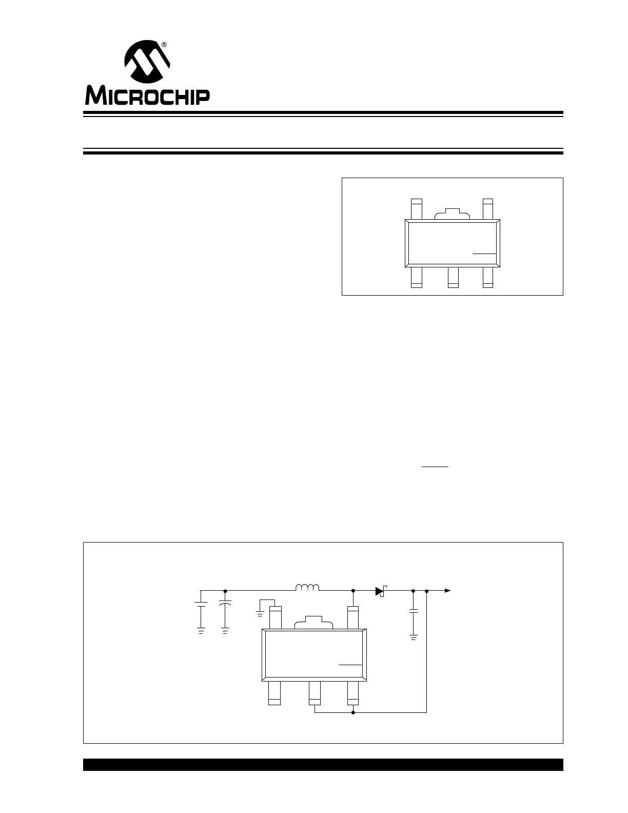
Package Type
General Description
The TC115 is a high-efficiency step-up DC/DC
converter for small, low input voltage or battery-
powered systems. This device has a start-up voltage
of 0.9V and a typical supply current of 80 µA. Phase
compensation and soft-start circuitry are included on-
chip. Unlike conventional PWM step-up converters,
the TC115 automatically shifts to pulse frequency
modulation (PFM) at low loads, resulting in reduced
supply current and improved efficiency.
The TC115 requires only an external diode, an inductor
and a capacitor, while supporting typical output cur-
rents of 140 mA. Supply current is reduced to less than
0.5 µA (max) when SHDN input is brought low.
Small size, low installed cost and low supply current
make the TC115 step-up converter ideal for use in a
wide range of battery-powered systems.
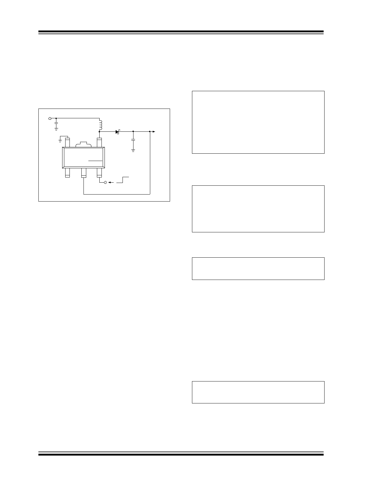
Functional Block Diagram
5
4
TC115
1
3
2
GND
LX
NC
PS
SHDN
SOT-89-5
PS
1.5V
C
1
10 µF
L
1
100 µH
Sumida
®
CD-54
1.5V to +3V, 50 mA Supply
5
4
TC115
1
3
2
SHDN
PS
NC
C
2
47 µF
Tantalum
IN5817
D
1
GND
LX
+3V
OUT
+
+
+
PS
PFM/PWM Step-Up DC/DC Converter
TC115
DS21361D-page 2
2002-2012 Microchip Technology Inc.
1.0
ELECTRICAL
CHARACTERISTICS
Absolute Maximum Ratings†
Power Supply Voltage (PS) ...............................................12V
Power Dissipation ......................................................500 mW
LX Sink Current......................................................400 mA pk
SHDN Input Voltage ..........................................................12V
Operating Temperature Range........................-40°C to +85°C
Storage Temperature Range .........................-40°C to +125°C
† Stresses above those listed under "Absolute Maximum
Ratings" may cause permanent damage to the device. These
are stress ratings only and functional operation of the device
at these or any other conditions above those indicated in the
operation sections of the specifications is not implied.
Exposure to Absolute Maximum Rating conditions for
extended periods may affect device reliability.
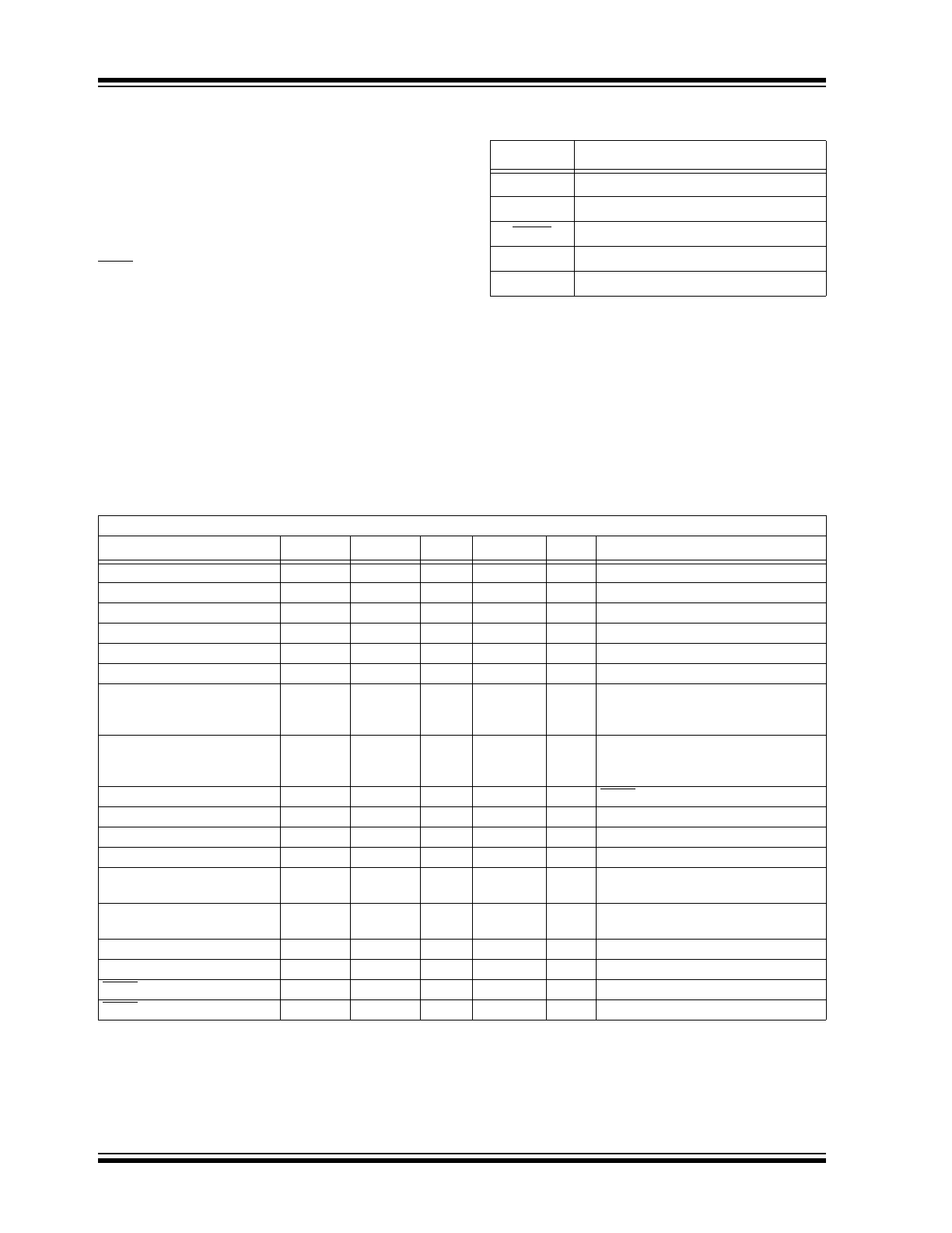
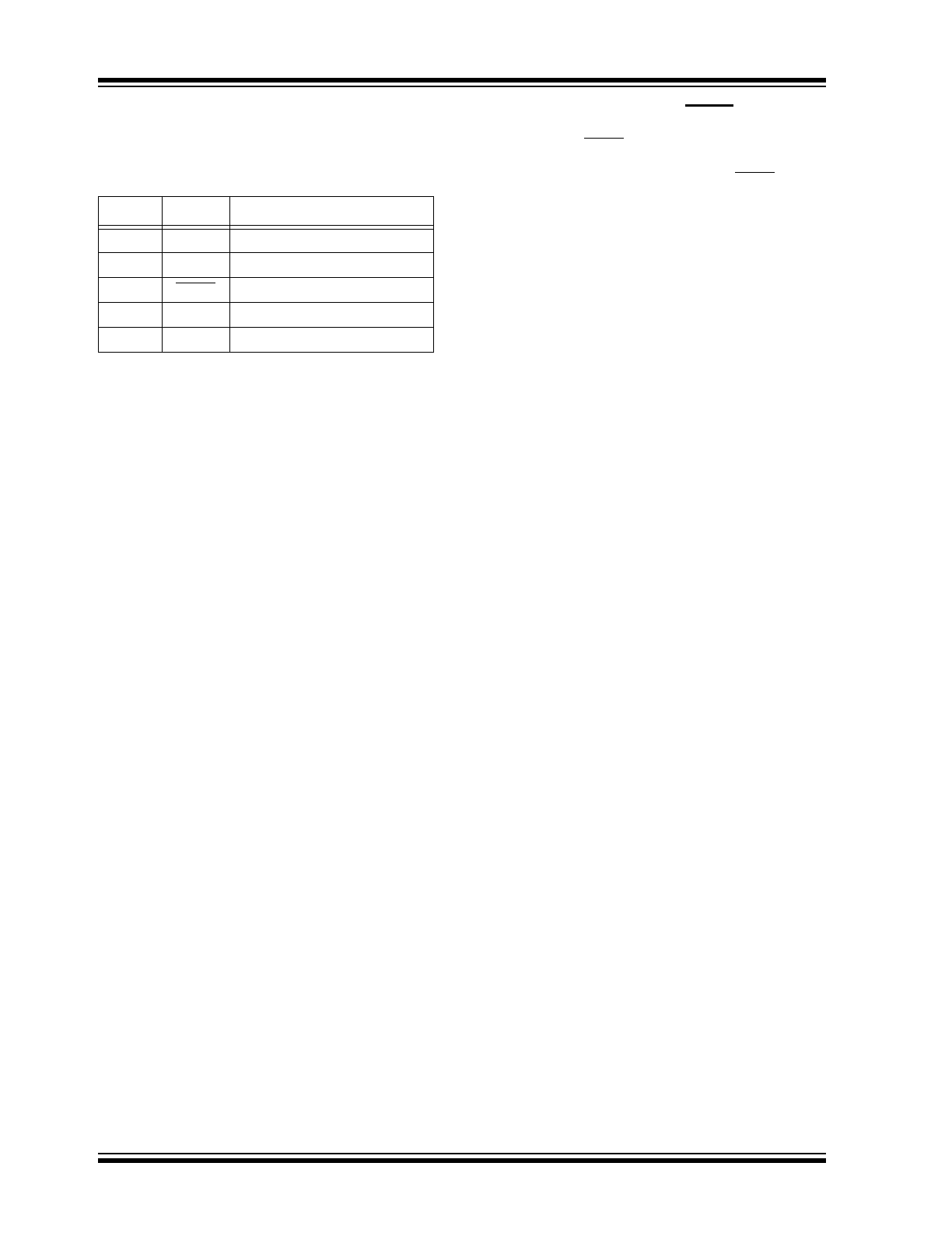
PIN FUNCTION TABLE
DC CHARACTERISTICS
Symbol
Description
NC
Not connected
PS
Power and voltage sense input
SHDN
Shutdown input
LX
Inductor switch output
GND
Ground terminal
Electrical Specifications: Unless otherwise noted, V
OUT
= 5V, T
A
= +25°C. Circuit configuration is illustrated in Figure 5-1.
Parameters
Sym
Min
Typ
Max
Units
Conditions
Operating Supply Voltage
V
IN
0.9
—
10.0
V
Note 5
Start-Up Supply Voltage
V
START
—
—
0.9
V
I
OUT
= 1 mA
LX Maximum Sink Current
I
LX
MAX
—
—
350
mA
LX Limit Frequency
f
LIM
—
200
—
kHz
V
LX
= VLX
LIM
LX Limit Voltage
VLX
LIM
0.7
—
1.3
V
Note 2
No Load Supply Current
I
DD
—
13
26
µA
I
OUT
= 0, V
IN
= V
OUT
x 0.8 (Note 3)
Boost Mode Supply Current
I
CC
—
80
135
µA
No external components,
V
IN
= (0.95 x V
OUT
) applied to PS (or
V
DD
) input
Standby Supply Current
I
STBY
—
9
17
µA
No external components,
V
IN
= (1.1 x V
OUT
) applied to PS
(or V
DD
) input
Shutdown Supply Current
I
SD
—
—
0.5
µA
SHDN = 0V
Oscillator Frequency
f
OSC
85
100
115
kHz
Note 2, Note 4
Output Voltage
V
OUT
V
R
x 0.975
V
R
V
R
x 1.025
V
V
IN
= 2.2V minimum (Note 1)
LX Output ON Resistance
Rswon
—
1.4
2.4
V
LX
= 0.4V
Duty Cycle
(PFM Operating Mode)
PFMDUTY
10
17
25
%
No external components
Maximum Duty Cycle
MAX-
DUTY
80
87
92
%
Note 4
Soft Start Time
t
SS
4
10
20
msec
Efficiency
h
—
85
—
%
SHDN Input Logic High
V
IH
0.75
—
—
V
SHDN Input Logic Low
V
IL
—
—
0.20
V
Note
1:
V
R
is the nominal factory-programmed output voltage setting.
2:
VLX
LIM
is the voltage on the LX pin (with internal switch ON) that will cause the oscillator to run at twice nominal
frequency in to limit the switch current through the internal N-channel switching transistor.
3:
Measured with D
1
= MA735 (reverse current < 1 µA at a reverse voltage of 10V).
4:
With TC115 operating in PWM mode.
5:
See Section 4.4, “Behavior When V
IN
is Greater Than the Factory-Programmed V
OUT
Setting”.
2002-2012 Microchip Technology Inc.
DS21361D-page 3
TC115
2.0
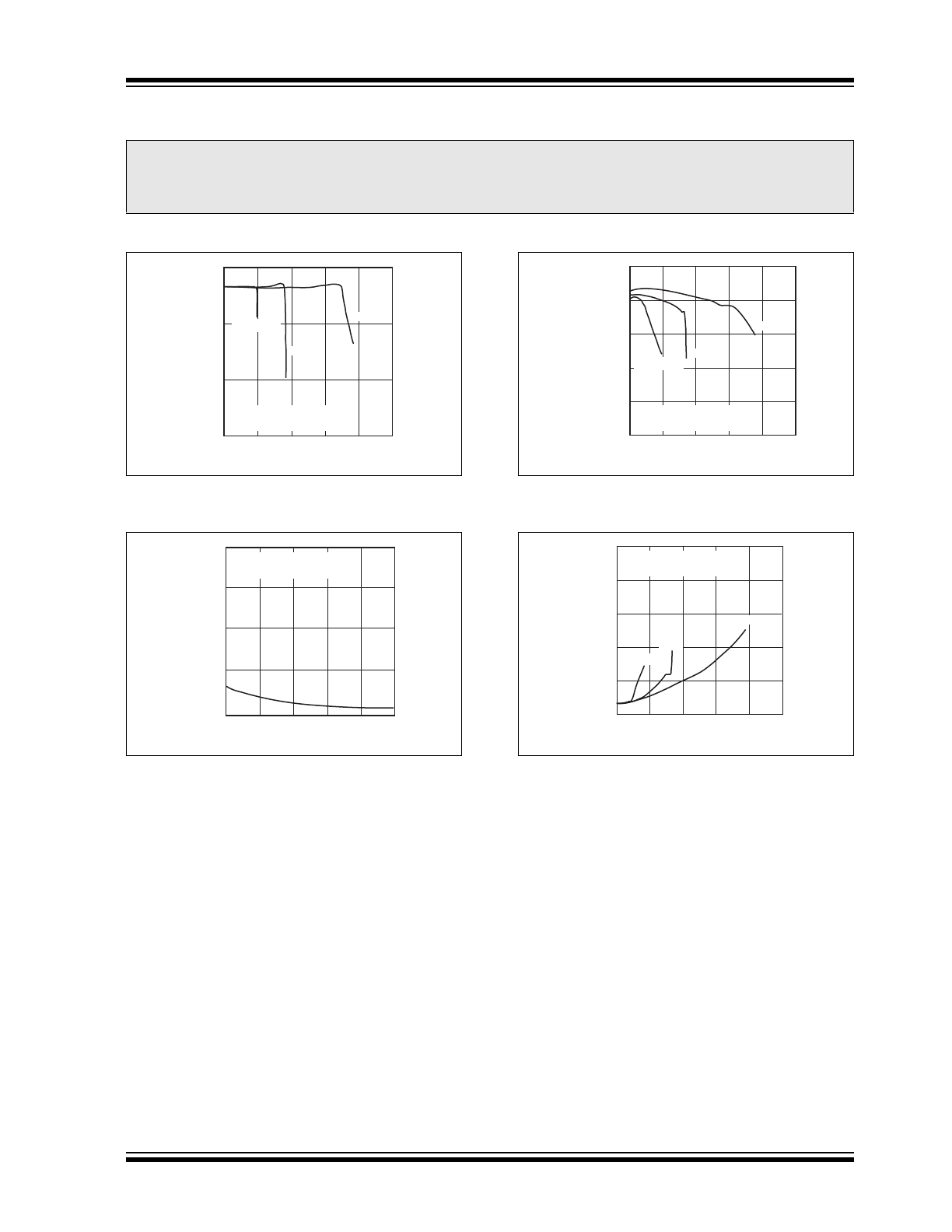
TYPICAL PERFORMANCE CURVES
Note: Unless otherwise indicated, V
OUT
= 5V, T
A
= +25°C.
FIGURE 2-1:
Output Voltage vs. Output
Current.
FIGURE 2-2:
No Load Input Current vs.
Input Voltage.
FIGURE 2-3:
Efficiency vs. Output
Current.
FIGURE 2-4:
Ripple Voltage vs. Output
Current.
Note:
The graphs and tables provided following this note are a statistical summary based on a limited number of
samples and are provided for informational purposes only. The performance characteristics listed herein
are not tested or guaranteed. In some graphs or tables, the data presented may be outside the specified
operating range (e.g., outside specified power supply range) and therefore outside the warranted range.
OUTPUT CURRENT I
OUT
(mA)
OUTPUT VOLTAGE V
OUT
(V)
0
40
80
120
160
200
3.1
2.9
2.7
2.5
1.5V
V
IN
= 1.0V
L
1
= 100
µH
C2 = 47
µF (Tantalum)
2.0V
1.0
1.2
1.4
1.6
1.8
2.0
INPUT VOLTAGE V
IN
(V)
200
INPUT CURRENT I
IN
(
µ
A) 150
100
50
0
L
1 = 100
µH
C2 = 47
µF (Tantalum)
OUTPUT CURRENT I
OUT
(mA)
EFFICIENCY (%)
0
40
80
120
160
200
100
80
60
40
20
0
V
IN
= 1.0V
1.5V
2.0V
L
1 = 100
µH
C2 = 47
µF (Tantalum)
OUTPUT CURRENT I
OUT
(mA)
RIPPLE VOLTAGE Vr(mVp-p)
0
40
80
120
160
200
100
80
60
40
10
0
L
1 = 100
µH
C2 = 47
µF (Tantalum)
2.0V
1.5V
V
IN
= 1.0V
TC115
DS21361D-page 4
2002-2012 Microchip Technology Inc.
3.0
PIN DESCRIPTIONS
The descriptions of the pins are listed in Table 3-1.
TABLE 3-1:
PIN FUNCTION TABLE
3.1
Power and Voltage Sense Input
(PS)
PS is a dual function input that provides both feedback
voltage sensing and internal chip power. It should be
connected to the regulator output (See Section 5.0,
“Applications”).
3.2
Shutdown Input (SHDN)
A logic-low on SHDN suspends device operation and
supply current is reduced to less than 0.5 µA. The
device resumes normal operation when SHDN is again
brought high.
3.3
Inductor Switch Output (LX)
LX is the drain of an internal N-channel switching tran-
sistor. This terminal drives the external inductor, which
ultimately provides current to the load.
3.4
Ground Terminal (GND)
Connect to circuit ground.
3.5
No Connect (NC)
No internal connection.
Pin No.
Symbol
Description
1
NC
Not connected
2
PS
Power and voltage sense input
3
SHDN
Shutdown input
4
LX
Inductor switch output
5
GND
Ground terminal

2002-2012 Microchip Technology Inc.
DS21361D-page 5
TC115
4.0
DETAILED DESCRIPTION
The TC115 is a combination PFM/PWM step-up
(boost) regulator. It is particularly useful in battery-pow-
ered 1, 2 and 3 cell applications where the required out-
put current is 140 mA or less, and size/cost issues are
a concern. The device operates in PWM mode when
the output load is sufficient to demand a 10% (or
greater) duty cycle. While in PWM mode, the TC115
behaves as any other PWM switching regulator to a
maximum duty cycle of 92%. At low output loads (i.e.,
output loads requiring < 10% duty cycle to support), the
TC115 automatically switches to pulse frequency mod-
ulation (PFM) operating mode with a fixed duty cycle of
25% (max) (17%, typical). While in PFM mode, the
inductor is modulated with individual fixed width pulses
only as needed to maintain output voltage. This action
reduces supply current, thereby improving power
efficiency at low output loads.
4.1
Input Power and Sensing
The TC115 is powered from the PS input, which must
be connected to the regulated output, as shown in
Figure 5-1. PS also senses output voltage for closed-
loop regulation. Start-up current is furnished through
the inductor when input voltage is initially applied. This
action starts the oscillator, causing the voltage at the
PS input to rise, bootstrapping the regulator into full
operation.
4.2
Output Diode
For best results, use a Schottky diode, such as the
MA735, 1N5817, EC10 or equivalent. Connect the
diode between the PS and LX pins as close to the IC as
possible. While ultra fast diodes can be used, lower effi-
ciency will result due to their higher forward voltage
drop. Ordinary rectifiers should be avoided because of
their slow recovery characteristics.
4.3
Low Power Shutdown Mode
The TC115 enters a low power shutdown mode when
SHDN is brought low. While in shutdown, the oscillator
is disabled and the internal switch is shut off. Normal
regulator operation resumes when SHDN is brought
high. SHDN may be tied to the input supply if not used.
4.4
Behavior When V
IN
is Greater
Than the Factory-Programmed
V
OUT
Setting
The TC115 is designed to operate as a step-up
regulator only. As such, V
IN
is assumed to always be
less than the factory-programmed V
OUT
setting (V
R
).
Operating the TC115 with V
IN
> V
R
causes regulating
action to be suspended (and corresponding supply
current reduction to 9 µA, typical) until V
IN
is again less
than V
R
. While regulating action is suspended, V
IN
is
connected to V
OUT
through the series combination of
the inductor and Schottky diode. Care must be taken to
add the appropriate isolation (MOSFET output switch
or post LDO with shutdown) during system design if
this V
IN
/V
OUT
leakage path is problematic.
Note:
Because the TC115 uses an external
diode, a leakage path between the input
voltage and the output node (through the
inductor and diode) exists while the regu-
lator is in shutdown. Care must be taken in
system design to assure the input supply
is isolated from the load during shutdown.
TC115
DS21361D-page 6
2002-2012 Microchip Technology Inc.
5.0
APPLICATIONS
5.1
Input Bypass Capacitors
Using an input bypass capacitor reduces peak current
transients drawn from the input supply and reduces the
switching noise generated by the regulator. The source
impedance of the input supply determines the size of
the capacitor that should be used.
FIGURE 5-1:
TC115 Typical Application.
5.2
Inductor Selection
Selecting the proper inductor value is a trade-off
between physical size and power conversion require-
ments. Lower value inductors cost less, but result in
higher ripple current and core losses. They are also
more prone to saturate since the coil current ramps to
a higher value. Larger inductor values reduce both
ripple current and core losses, but are larger in physical
size and tend to increase the start-up time slightly.
Practical inductor values, therefore, range from 50 µH
to 300 µH. Inductors with a ferrite core (or equivalent)
are recommended. For highest efficiency, use an
inductor with a series resistance less than 0.1
).
The inductor value directly affects the output ripple
voltage. Equation 5-3 is derived as shown below, and
can be used to calculate an inductor value, given the
required output ripple voltage (V
RIPPLE
) and output
capacitor series resistance:
EQUATION 5-1:
Expressing di in terms of switch ON resistance and
time:
EQUATION 5-2:
Solving for L:
EQUATION 5-3:
Care must be taken to ensure the inductor can handle
peak switching currents, which can be several times
load currents. Exceeding rated peak current will result
in core saturation and loss of inductance. The inductor
should be selected to withstand currents greater than
I
PK
(Equation 5-10) without saturating.
Calculating the peak inductor current is straightforward.
Inductor current consists of an AC (sawtooth) current
centered on an average DC current (i.e., input current).
Equation 5-6 calculates the average DC current. Note
that minimum input voltage and maximum load current
values should be used:
EQUATION 5-4:
C
1
L
1
5
4
TC115
1
3
2
SHDN
PS
NC
C
2
D
1
GND
LX
V
OUT
V
IN
OFF ON
(Tie to V
IN
or V
OUT
if not used)
+
+
Where:
ESR: the equivalent series resistance of the
output filter capacitor; V
RIPPLE
is in
volts.
di: represents the peak to peak ripple
current in the inductor.
V
RIPPLE
ESR di
V
RIPPLE
V
IN
V
SW
–
t
ON
L
--------------------------------------------
Where:
V
SW
= voltage drop across the switch.
T
ON
= the amount of time the switch is ON.
L
V
IN
V
SW
–
t
ON
V
R IP PLE
--------------------------------------------
Input Power
Output Power
Efficiency
---------------------------------
=
2002-2012 Microchip Technology Inc.
DS21361D-page 7
TC115
Rewriting in terms of input and output currents and volt-
ages:
EQUATION 5-5:
Solving for input current:
EQUATION 5-6:
The sawtooth current is centered on the DC current
level, swinging equally above and below the DC current
calculated in Equation 5-6. The peak inductor current is
the sum of the DC current plus half the ac current. Note
that minimum input voltage should be used when
calculating the ac inductor current (Equation 5-9).
EQUATION 5-7:
EQUATION 5-8:
EQUATION 5-9:
Combining the DC current calculated in Equation 5-6,
with half the peak ac current calculated in Equation 5-9,
the peak inductor current is given by:
EQUATION 5-10:
5.3
Internal Transistor Switch
The LX pin has a typical ON resistance of 1.4
.
Therefore, peak switch current is given by (V
IN
/1.4).
The internal transistor switch has a maximum design
rating of 350 mA. An oscillator frequency doubling cir-
cuit is an included guard against high switching cur-
rents. Should the voltage on the LX pin rise above 1.3V
(max) while the internal N-channel switch is ON, the
oscillator frequency automatically doubles to minimize
ON time. Although reduced, switch current still flows
because the PWM remains in operation. Therefore, the
LX input is not internally current-limited and care must
be taken never to exceed the 350 mA maximum limit.
Failure to observe this will result in damage to the
regulator.
5.4
Output Capacitor
The effective series resistance of the output capacitor
directly affects the amplitude of the output voltage
ripple (The product of the peak inductor current and the
ESR determines output ripple amplitude). Therefore, a
capacitor with the lowest possible ESR should be
selected. Smaller capacitors are acceptable for light
loads (or in applications where ripple is not a concern).
The Sprague
®
595D series of tantalum capacitors are
among the smallest of all low ESR surface mount
capacitors available. Table 5-1 lists suggested
components and suppliers.
5.5
Board Layout Guidelines
As with all inductive switching regulators, the TC115
generates fast switching waveforms which radiate
noise. Interconnecting lead lengths should be
minimized to keep stray capacitance, trace resistance
and radiated noise as low as possible. In addition, the
GND pin, input bypass capacitor and output filter
capacitor ground leads should be connected to a single
point.
TABLE 5-1:
SUGGESTED COMPONENTS AND SUPPLIERS
V
IN
M IN
I
IN
M A X
V
OUT
MA X
I
OUT
M AX
Efficiency
---------------------------------------------------
=
I
IN
M A X
V
OUT
M A X
I
OUT
MA X
Efficiency
V
IN
M IN
----------------------------------------------------
=
V
L
L di dt
=
di
V
L
di dt
=
di
V
IN
M IN
V
SW
–
t
ON
L
----------------------------------------------
=
Where:
V
SW
= The voltage drop across the internal
N-channel MOSFET.
I
P K
I
IN
M A X
0.5 di
+
=
Type
Inductors
Capacitors
Diodes
Surface Mount
Sumida
®
CD54 Series
CDR125 Series
Coiltronics™
CTX Series
Matsuo
®
267 Series
Sprague
®
595D Series
Nichicon™
F93 Series
Nihon
EC10 Series
Matsushita™
MA735 Series
Through-Hole
Sumida
®
RCH855 Series
RCH110 Series
Renco
®
RL1284-12
Sanyo™
OS-CON Series
Nichicon™
PL Series
ON Semiconductor
®
1N5817 - 1N5822
TC115
DS21361D-page 8
2002-2012 Microchip Technology Inc.
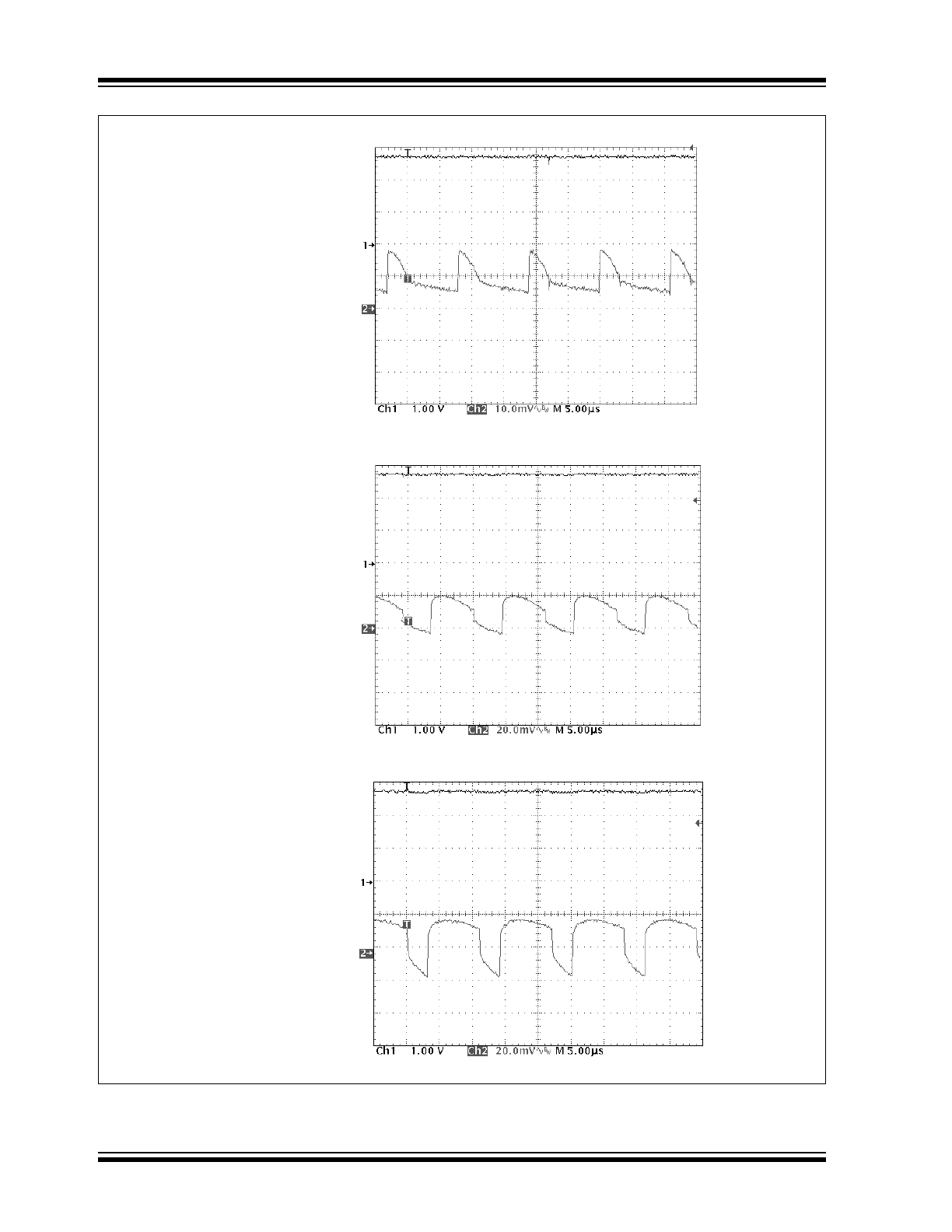
FIGURE 5-2:
Typical Ripple Waveforms.
TC115301
V
IN
= 2.5V
I
LOAD
= 80 mA
CH1: V
OUT
(DC)
CH2: V
OUT
(AC Ripple)
L = 100
µH
C = 47
µF
D1 = MA735
TC115301
V
IN
= 2.0V
I
LOAD
= 40 mA
CH1: V
OUT
(DC)
CH2: V
OUT
(AC Ripple)
L = 100
µH
C = 47
µF
D1 = MA735
TC115301
V
IN
= 1.0V
I
LOAD
= 10 mA
CH1: V
OUT
(DC)
CH2: V
OUT
(AC Ripple)
L = 100
µH
C = 47
µF
D1 = MA735
2002-2012 Microchip Technology Inc.
DS21361D-page 9
TC115
6.0
PACKAGING INFORMATION
6.1
Package Marking Information
Example: For TC115331, the marking code is:
Symbol
(100 kHz)
Voltage
1
1.
2
2.
3
3.
4
4.
5
5.
6
6.
Symbol
(100 kHz)
Voltage
0
.0
1
.1
2
.2
3
.3
4
.4
5
.5
6
.6
7
.7
8
.8
9
.9
5
4
1
3
2
SOT-89-5
4
1
3
2
1
represents product classification; TC115 = 1
2
represents first integer of voltage and frequency
3
represents first decimal of voltage and frequency
4
represents production lot ID code
3
X
1
3
TC115
DS21361D-page 10
2002-2012 Microchip Technology Inc.
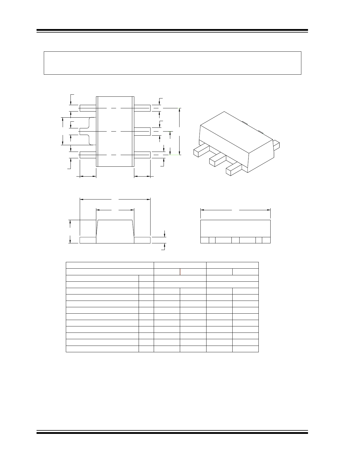
5-Lead Plastic Small Outline Transistor Header (MT) (SOT-89)
0.53
0.41
.021
.016
B
Lead 2 Width
0.44
0.37
.017
.015
c
Lead Thickness
1.80
1.40
.071
.055
D1
Tab Width
4.60
4.40
.181
.173
D
Overall Length
4.50
.177
H
Overall Width
1.60
1.40
.063
.055
A
Overall Height
3.00 BSC
.118 BSC
p1
Outside lead pitch (basic)
1.50 BSC
.059 BSC
p
Pitch
MAX
MIN
MAX
MIN
Dimension Limits
MILLIMETERS*
INCHES
Units
exceed .005" (0.127mm) per side.
Dimensions D and E1 do not include mold flash or protrusions. Mold flash or protrusions shall not
Notes:
Drawing No. C04-030
*Controlling Parameter
Foot Length
L
.031
0.80
Leads 1,3, 4 & 5 Width
B1
.014
.019
0.36
0.48
Molded Package Width
E
.090
.102
2.29
2.60
-
-
-
-
Tab Lead Width
B2
.013
.019
0.32
0.48
D1
H
L
B1
B
B1
p
p1
E
C
A
1
2
2
3
L
B1
B1
4
5
B2
D
Note:
For the most current package drawings, please see the Microchip Packaging Specification located
at http://www.microchip.com/packaging