
2002-2012 Microchip Technology Inc.
DS21357C-page 1
TC1108
Features
• Extremely Low Supply Current (50
A, Typ.)
• Very Low Dropout Voltage
• 300mA Output Current
• High Output Voltage Accuracy
• Standard or Custom Output Voltages
• Over Current and Over Temperature Protection
Applications
• Battery Operated Systems
• Portable Computers
• Medical Instruments
• Instrumentation
• Cellular/GSM/PHS Phones
• Linear Post-Regulators for SMPS
• Pagers
Device Selection Table
NOTE: xx indicates output voltages
Available Output Voltages: 2.5, 2.8, 3.0, 3.3, 5.0.
Other output voltages are available. Please contact Microchip
Technology Inc. for details.
Package Type
General Description
The TC1108 is a fixed output, high accuracy (typically
±0.5%) CMOS low dropout regulator. Total supply
current is typically 50
A at full load (20 to 60 times
lower than in bipolar regulators).
TC1108 key features include ultra low noise operation,
very low dropout voltage (typically 240mV at full load),
and fast response to step changes in load.
The TC1108 incorporates both over temperature and
over current protection. The TC1108 is stable with an
output capacitor of only 1
F and has a maximum
output current of 300mA. It is available in a SOT-223
package.
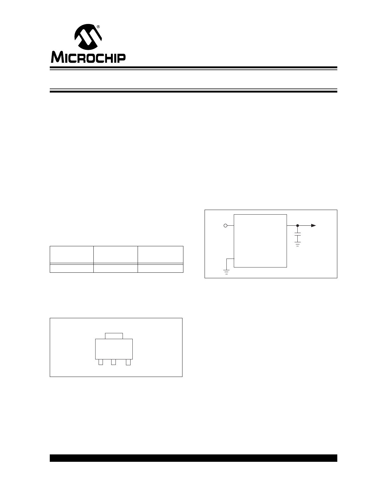
Typical Application
Part Number
Package
Junction
Temp. Range
TC1108-xxVDB
3-Pin SOT-223
-40°C to +125°C
SOT-223
3
2
1
V
OUT
GND
V
IN
TC1108VDB
TC1108
1
2
3
V
IN
V
OUT
C1
1
μF
GND
V
OUT
V
IN
+
300mA CMOS LDO
TC1108
DS21357C-page 2
2002-2012 Microchip Technology Inc.
1.0
ELECTRICAL
CHARACTERISTICS
Absolute Maximum Ratings*
Input Voltage .........................................................6.5V
Output Voltage.................. (V
SS
– 0.3V) to (V
IN
+ 0.3V)
Power Dissipation................Internally Limited (Note 6)
Maximum Voltage on Any Pin ........ V
IN
+0.3V to -0.3V
Operating Temperature Range...... -40°C < T
J
< 125°C
Storage Temperature..........................-65°C to +150°C
Stresses above those listed under "Absolute Maximum
Ratings" may cause permanent damage to the device. These
are stress ratings only and functional operation of the device
at these or any other conditions above those indicated in the
operation sections of the specifications is not implied.
Exposure to Absolute Maximum Rating conditions for
extended periods may affect device reliability.
TC1108 ELECTRICAL SPECIFICATIONS
Electrical Characteristics: V
IN
= V
OUT
+ 1V, I
L
= 100
A, C
L
= 3.3
F, T
A
= 25°C, unless otherwise noted. Boldface type
specifications apply for junction temperatures of -40°C to +125°C.
Symbol
Parameter
Min
Typ
Max
Units
Test Conditions
V
IN
Input Operating Voltage
2.7
—
6.0
V
Note 7
I
OUT
MAX
Maximum Output Current
300
—
—
mA
V
OUT
Output Voltage
—
V
R
– 2.5%
V
R
±0.5%
—
—
V
R
+ 2.5%
V
Note 1
V
OUT
/
T
V
OUT
Temperature Coefficient
—
40
—
ppm/°C Note 2
V
OUT
/
V
IN
Line Regulation
—
0.05
0.35
%
(V
R
+ 1V)
V
IN
6V
V
OUT
/V
OUT
Load Regulation
—
0.5
2.0
%
I
L
= 0.1mA to I
OUT
MAX
(Note 3)
V
IN
-V
OUT
Dropout Voltage
—
—
—
20
80
240
30
160
480
mV
I
L
= 0.1mA
I
L
= 100mA
I
L
= 300mA (Note 4)
I
DD
Supply Current
—
50
90
A
PSRR
Power Supply Rejection Ratio
—
60
—
dB
F
RE
1kHz
I
OUT
SC
Output Short Circuit Current
—
550
650
mA
V
OUT
= 0V
V
OUT
/
P
D
Thermal Regulation
—
0.04
—
V/W
Note 5
eN
Output Noise
—
260
—
nV/
Hz F = 10kHz, C
OUT
= 1
F,
R
LOAD
= 50
Note
1:
V
R
is the regulator output voltage setting.
2:
3:
Regulation is measured at a constant junction temperature using low duty cycle pulse testing. Load regulation is tested over a load range
from 0.1mA to the maximum specified output current. Changes in output voltage due to heating effects are covered by the thermal
regulation specification.
4:
Dropout voltage is defined as the input to output differential at which the output voltage drops 2% below its nominal value measured at a
1V differential.
5:
Thermal Regulation is defined as the change in output voltage at a time T after a change in power dissipation is applied, excluding load or
line regulation effects. Specifications are for a current pulse equal to I
L
MAX
at V
IN
= 6V for T = 10 msec.
6:
The maximum allowable power dissipation is a function of ambient temperature, the maximum allowable junction temperature and the
thermal resistance from junction-to-air (i.e., T
A
, T
J
,
JA
). Exceeding the maximum allowable power dissipation causes the device to initiate
thermal shutdown. Please see Section 4.0 Thermal Considerations for more details.
7:
The minimum V
IN
has to justify the conditions: V
IN
V
R
+ V
DROPOUT
and V
IN
2.7V for I
L
= 0.1mA to I
OUT
MAX
.
TC V
OUT
= (V
OUT
MAX
– V
OUT
MIN
) x 10
6
V
OUT
x
T
2002-2012 Microchip Technology Inc.
DS21357C-page 3
TC1108
2.0
PIN DESCRIPTIONS
The descriptions of the pins are listed in Table 2-1.
TABLE 2-1:
PIN FUNCTION TABLE
3.0
DETAILED DESCRIPTION
The TC1108 is a precision, fixed output LDO. Unlike
bipolar regulators, the TC1108’s supply current does
not increase with load current. In addition, V
OUT
remains stable and within regulation over the entire
0mA to I
OUT
MAX
operating load current range, (an
important consideration in RTC and CMOS RAM
battery back-up applications).
Figure 3-1 shows a typical application circuit.
FIGURE 3-1:
TYPICAL APPLICATION
CIRCUIT
3.1
Output Capacitor
A 1
F (min) capacitor from V
OUT
to ground is required.
The output capacitor should have an effective series
resistance greater than 0.1
and less than 5.0. A 1F
capacitor should be connected from V
IN
to GND if there
is more than 10 inches of wire between the regulator
and the AC filter capacitor, or if a battery is used as the
power source. Aluminum electrolytic or tantalum
capacitor types can be used. (Since many aluminum
electrolytic capacitors freeze at approximately -30°C,
solid tantalums are recommended for applications
operating below -25°C.) When operating from sources
other than batteries, supply-noise rejection and
transient response can be improved by increasing the
value of the input and output capacitors and employing
passive filtering techniques.
Pin No.
(3-Pin SOT-223)
Symbol
Description
1
V
IN
Unregulated supply input.
2
GND
Ground terminal.
3
V
OUT
Regulated voltage output.
C1
1
μF
Battery
TC1108
1
2
3
V
IN
V
OUT
C2
1
μF
GND
V
OUT
+
–
+
+
TC1108
DS21357C-page 4
2002-2012 Microchip Technology Inc.
4.0
THERMAL CONSIDERATIONS
4.1
Thermal Shutdown
Integrated thermal protection circuitry shuts the
regulator off when die temperature exceeds 150°C.
The regulator remains off until the die temperature
drops to approximately 140°C.
4.2
Power Dissipation
The amount of power the regulator dissipates is
primarily a function of input and output voltage, and
output current. The following equation is used to
calculate worst case actual power dissipation:
EQUATION 4-1:
The maximum allowable power dissipation (Equation
4-2) is a function of the maximum ambient temperature
(T
A
MAX
), the maximum allowable die temperature
(T
J
MAX
) and the thermal resistance from junction-to-air
(
JA
).
EQUATION 4-2:
Table 4-1 shows various values of
JA
for the TC1108
versus board copper area.
TABLE 4-1:
THERMAL RESISTANCE
GUIDELINES FOR TC1108
NOTE: *Tab of device attached to topside copper
Equation 4-1 can be used in conjunction with Equation
4-2 to ensure regulator thermal operation is within
limits. For example:
Given:
V
IN
MAX
= 3.3V + 10%
V
OUT
MIN
= 2.7V – 0.5%
I
LOAD
MAX
= 275mA
T
J
MAX
= 125°C
T
A
MAX
= 95°C
JA
= 59°C/W
Find: 1. Actual power dissipation
2. Maximum allowable dissipation
Actual power dissipation:
P
D
(V
IN
MAX
– V
OUT
MIN
)I
LOAD
MAX
= [(3.3 x 1.1) – (2.7 x .995)]275 x 10
–3
= 260mW
Maximum allowable power dissipation:
In this example, the TC1108 dissipates a maximum of
260mW; below the allowable limit of 508mW. In a
similar manner, Equation 4-1 and Equation 4-2 can be
used to calculate maximum current and/or input
voltage limits. For example, the maximum allowable
V
IN
, is found by sustituting the maximum allowable
power dissipation of 508mW into Equation 4-1, from
which V
IN
MAX
= 4.6V.
Copper
Area
(Topside)*
Copper
Area
(Backside)
Board
Area
Thermal
Resistance
(
JA
)
2500 sq mm
2500 sq mm 2500 sq mm
45°C/W
1000 sq mm
2500 sq mm 2500 sq mm
45°C/W
225 sq mm
2500 sq mm 2500 sq mm
53°C/W
100 sq mm
2500 sq mm 2500 sq mm
59°C/W
1000 sq mm
1000 sq mm 1000 sq mm
52°C/W
1000 sq mm
0 sq mm
1000 sq mm
55°C/W
Where:
P
D
(V
IN
MAX
– V
OUT
MIN
)I
LOAD
MAX
V
IN
MAX
V
OUT
MIN
I
LOAD
MAX
= Worst case actual power dissipation
= Minimum regulator output voltage
= Maximum output (load) current
= Maximum voltage on V
IN
P
D
P
D
MAX
= (T
J
MAX
– T
A
MAX
)
JA
Where all terms are previously defined.
P
D
MAX
= (T
J
MAX
– T
A
MAX
)
JA
= (125 – 95)
59
= 508mW
2002-2012 Microchip Technology Inc.
DS21357C-page 5
TC1108
5.0
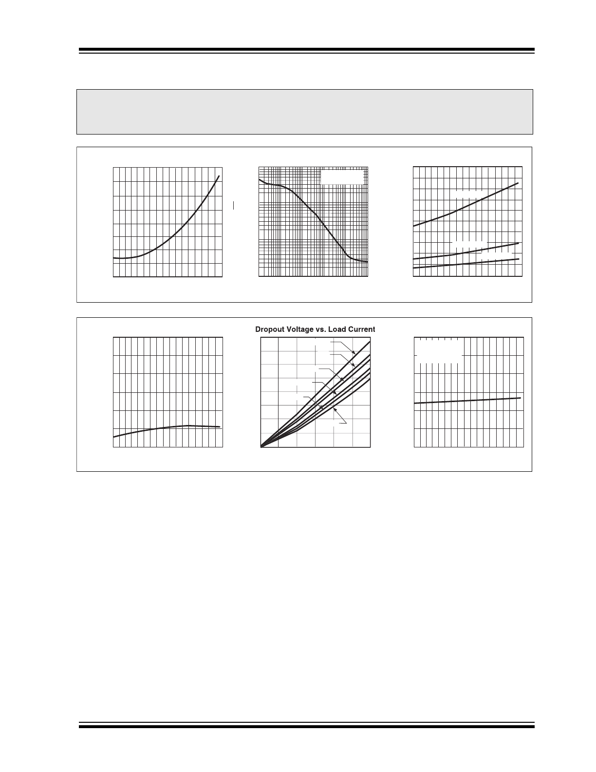
TYPICAL CHARACTERISTICS
Note:
The graphs and tables provided following this note are a statistical summary based on a limited number of
samples and are provided for informational purposes only. The performance characteristics listed herein are
not tested or guaranteed. In some graphs or tables, the data presented may be outside the specified
operating range (e.g., outside specified power supply range) and therefore outside the warranted range.
Output Noise
FREQUENCY (kHz)
NOISE (
μ
V/
√
HZ)
10.0
1.0
0.01
0.01
1
10
100
1000
0.1
0.0
R
LOAD
= 50Ω
C
OUT
= 1
μF
0.012
0.010
0.008
0.004
0.002
0.000
-0.002
-0.004
0.006
-40
° -20° 0° 20° 40° 60° 80° 100° 120°
TEMPERATURE (
°
C)
Line Regulation
LINE REGULATION (%)
2.00
1.80
1.60
1.20
1.00
0.80
0.60
0.40
0.20
0.00
1.40
-40
° -20° 0° 20° 40° 60° 80° 100° 120°
TEMPERATURE (
°
C)
Load Regulation
LOAD REGULATION (%)
1 to 300mA
1 to 50mA
1 to 100mA
0.40
0.35
0.30
0.25
0.20
0.15
0.10
0.05
0.00
0
50
100
150
200
250
300
LOAD CURRENT (mA)
DROPOUT VOLTAGE (V)
100.0
90.0
70.0
80.0
50.0
40.0
60.0
-40
° -20° 0° 20° 40° 60° 80° 100° 120°
TEMPERATURE (
°C)
Supply Current
SUPPLY CURRENT (
μ
A)
3.075
3.025
2.925
2.975
-40
° -20° 0° 20° 40° 60° 80° 100° 120°
TEMPERATURE (
°C)
V
OUT
vs. Temperature
V
OUT
(V)
125
°C
8
85
°C
C
70
°C
25
°C
0
°C
C
-40
°C
V
IN
= 4V
I
LOAD
= 100μA
C
LOAD
= 3.3
μF
TC1108
DS21357C-page 6
2002-2012 Microchip Technology Inc.
6.0
PACKAGING INFORMATION
6.1
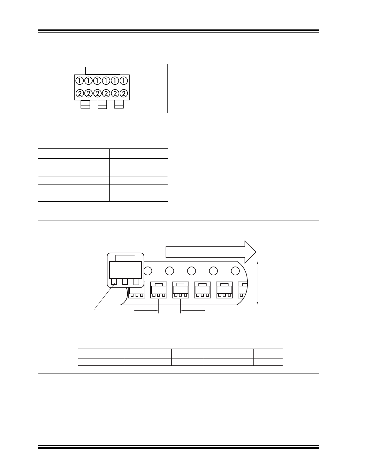
Package Marking Information
“1” = part number code
“2” = represents temperature + date code + lot identity
+ subcontractor identity
6.2
Taping Form
TC1108 (V)
Code
TC1108-2.5VDB
110825
TC1108-2.8VDB
110828
TC1108-3.0VDB
110830
TC1108-3.3VDB
110833
TC1108-5.0VDB
110850
Component Taping Orientation for 3-Pin SOT-223 Devices
Package
Carrier Width (W)
Pitch (P)
Part Per Full Reel
Reel Size
3-Pin SOT-223
12 mm
8 mm
4000
13 in
Carrier Tape, Number of Components Per Reel and Reel Size
User Direction of Feed
Device
Marking
PIN 1
Standard Reel Component Orientation
for TR Suffix Device
(Mark Right Side Up)
W
P
2002-2012 Microchip Technology Inc.
DS21357C-page 7
TC1108
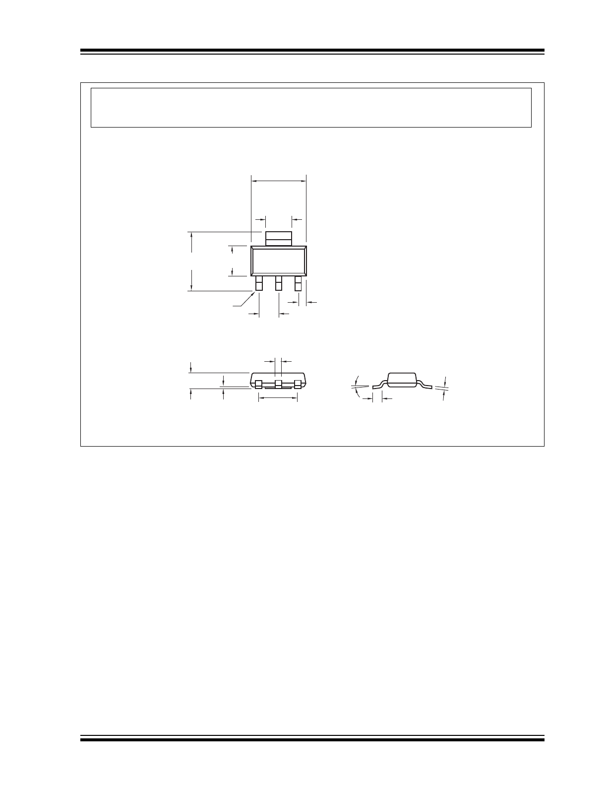
6.3
Package Dimensions
.264 (6.70)
.248 (6.30)
.122 (3.10)
.114 (2.90)
.287 (7.30)
.264 (6.70)
.146 (3.70)
.130 (3.30)
.091 (2.30) TYP.
.071
(1.80)
MAX.
.181 (4.60) TYP.
.036 (0.91) MIN.
.041 (1.04)
.033 (0.84)
PIN 1
.013 (0.33)
.009 (0.24)
.031 (0.80)
.024 (0.60)
.004 (0.10)
.001 (0.02)
10
°
MAX.
3-Pin SOT-223
Dimensions: inches (mm)
Note:
For the most current package drawings, please see the Microchip Packaging Specification located
at http://www.microchip.com/packaging

TC1108
DS21357C-page 8
2002-2012 Microchip Technology Inc.
REVISION HISTORY
Revision C (November 2012)
Added a note to the package outline drawing.
2002-2012 Microchip Technology Inc.
DS21357C-page 9
TC1108
SALES AND SUPPORT
Data Sheets
Products supported by a preliminary Data Sheet may have an errata sheet describing minor operational differences and recom-
mended workarounds. To determine if an errata sheet exists for a particular device, please contact one of the following:
1.
Your local Microchip sales office
2.
The Microchip Worldwide Site (www.microchip.com)
Please specify which device, revision of silicon and Data Sheet (include Literature #) you are using.
New Customer Notification System
Register on our web site (www.microchip.com/cn) to receive the most current information on our products.

TC1108
DS21357C-page 10
2002-2012 Microchip Technology Inc.
NOTES:
2002-2012 Microchip Technology Inc.
DS21357C-page 1
TC1108
Features
• Extremely Low Supply Current (50
A, Typ.)
• Very Low Dropout Voltage
• 300mA Output Current
• High Output Voltage Accuracy
• Standard or Custom Output Voltages
• Over Current and Over Temperature Protection
Applications
• Battery Operated Systems
• Portable Computers
• Medical Instruments
• Instrumentation
• Cellular/GSM/PHS Phones
• Linear Post-Regulators for SMPS
• Pagers
Device Selection Table
NOTE: xx indicates output voltages
Available Output Voltages: 2.5, 2.8, 3.0, 3.3, 5.0.
Other output voltages are available. Please contact Microchip
Technology Inc. for details.
Package Type
General Description
The TC1108 is a fixed output, high accuracy (typically
±0.5%) CMOS low dropout regulator. Total supply
current is typically 50
A at full load (20 to 60 times
lower than in bipolar regulators).
TC1108 key features include ultra low noise operation,
very low dropout voltage (typically 240mV at full load),
and fast response to step changes in load.
The TC1108 incorporates both over temperature and
over current protection. The TC1108 is stable with an
output capacitor of only 1
F and has a maximum
output current of 300mA. It is available in a SOT-223
package.
Typical Application
Part Number
Package
Junction
Temp. Range
TC1108-xxVDB
3-Pin SOT-223
-40°C to +125°C
SOT-223
3
2
1
V
OUT
GND
V
IN
TC1108VDB
TC1108
1
2
3
V
IN
V
OUT
C1
1
μF
GND
V
OUT
V
IN
+
300mA CMOS LDO
TC1108
DS21357C-page 2
2002-2012 Microchip Technology Inc.
1.0
ELECTRICAL
CHARACTERISTICS
Absolute Maximum Ratings*
Input Voltage .........................................................6.5V
Output Voltage.................. (V
SS
– 0.3V) to (V
IN
+ 0.3V)
Power Dissipation................Internally Limited (Note 6)
Maximum Voltage on Any Pin ........ V
IN
+0.3V to -0.3V
Operating Temperature Range...... -40°C < T
J
< 125°C
Storage Temperature..........................-65°C to +150°C
Stresses above those listed under "Absolute Maximum
Ratings" may cause permanent damage to the device. These
are stress ratings only and functional operation of the device
at these or any other conditions above those indicated in the
operation sections of the specifications is not implied.
Exposure to Absolute Maximum Rating conditions for
extended periods may affect device reliability.
TC1108 ELECTRICAL SPECIFICATIONS
Electrical Characteristics: V
IN
= V
OUT
+ 1V, I
L
= 100
A, C
L
= 3.3
F, T
A
= 25°C, unless otherwise noted. Boldface type
specifications apply for junction temperatures of -40°C to +125°C.
Symbol
Parameter
Min
Typ
Max
Units
Test Conditions
V
IN
Input Operating Voltage
2.7
—
6.0
V
Note 7
I
OUT
MAX
Maximum Output Current
300
—
—
mA
V
OUT
Output Voltage
—
V
R
– 2.5%
V
R
±0.5%
—
—
V
R
+ 2.5%
V
Note 1
V
OUT
/
T
V
OUT
Temperature Coefficient
—
40
—
ppm/°C Note 2
V
OUT
/
V
IN
Line Regulation
—
0.05
0.35
%
(V
R
+ 1V)
V
IN
6V
V
OUT
/V
OUT
Load Regulation
—
0.5
2.0
%
I
L
= 0.1mA to I
OUT
MAX
(Note 3)
V
IN
-V
OUT
Dropout Voltage
—
—
—
20
80
240
30
160
480
mV
I
L
= 0.1mA
I
L
= 100mA
I
L
= 300mA (Note 4)
I
DD
Supply Current
—
50
90
A
PSRR
Power Supply Rejection Ratio
—
60
—
dB
F
RE
1kHz
I
OUT
SC
Output Short Circuit Current
—
550
650
mA
V
OUT
= 0V
V
OUT
/
P
D
Thermal Regulation
—
0.04
—
V/W
Note 5
eN
Output Noise
—
260
—
nV/
Hz F = 10kHz, C
OUT
= 1
F,
R
LOAD
= 50
Note
1:
V
R
is the regulator output voltage setting.
2:
3:
Regulation is measured at a constant junction temperature using low duty cycle pulse testing. Load regulation is tested over a load range
from 0.1mA to the maximum specified output current. Changes in output voltage due to heating effects are covered by the thermal
regulation specification.
4:
Dropout voltage is defined as the input to output differential at which the output voltage drops 2% below its nominal value measured at a
1V differential.
5:
Thermal Regulation is defined as the change in output voltage at a time T after a change in power dissipation is applied, excluding load or
line regulation effects. Specifications are for a current pulse equal to I
L
MAX
at V
IN
= 6V for T = 10 msec.
6:
The maximum allowable power dissipation is a function of ambient temperature, the maximum allowable junction temperature and the
thermal resistance from junction-to-air (i.e., T
A
, T
J
,
JA
). Exceeding the maximum allowable power dissipation causes the device to initiate
thermal shutdown. Please see Section 4.0 Thermal Considerations for more details.
7:
The minimum V
IN
has to justify the conditions: V
IN
V
R
+ V
DROPOUT
and V
IN
2.7V for I
L
= 0.1mA to I
OUT
MAX
.
TC V
OUT
= (V
OUT
MAX
– V
OUT
MIN
) x 10
6
V
OUT
x
T
2002-2012 Microchip Technology Inc.
DS21357C-page 3
TC1108
2.0
PIN DESCRIPTIONS
The descriptions of the pins are listed in Table 2-1.
TABLE 2-1:
PIN FUNCTION TABLE
3.0
DETAILED DESCRIPTION
The TC1108 is a precision, fixed output LDO. Unlike
bipolar regulators, the TC1108’s supply current does
not increase with load current. In addition, V
OUT
remains stable and within regulation over the entire
0mA to I
OUT
MAX
operating load current range, (an
important consideration in RTC and CMOS RAM
battery back-up applications).
Figure 3-1 shows a typical application circuit.
FIGURE 3-1:
TYPICAL APPLICATION
CIRCUIT
3.1
Output Capacitor
A 1
F (min) capacitor from V
OUT
to ground is required.
The output capacitor should have an effective series
resistance greater than 0.1
and less than 5.0. A 1F
capacitor should be connected from V
IN
to GND if there
is more than 10 inches of wire between the regulator
and the AC filter capacitor, or if a battery is used as the
power source. Aluminum electrolytic or tantalum
capacitor types can be used. (Since many aluminum
electrolytic capacitors freeze at approximately -30°C,
solid tantalums are recommended for applications
operating below -25°C.) When operating from sources
other than batteries, supply-noise rejection and
transient response can be improved by increasing the
value of the input and output capacitors and employing
passive filtering techniques.
Pin No.
(3-Pin SOT-223)
Symbol
Description
1
V
IN
Unregulated supply input.
2
GND
Ground terminal.
3
V
OUT
Regulated voltage output.
C1
1
μF
Battery
TC1108
1
2
3
V
IN
V
OUT
C2
1
μF
GND
V
OUT
+
–
+
+
TC1108
DS21357C-page 4
2002-2012 Microchip Technology Inc.
4.0
THERMAL CONSIDERATIONS
4.1
Thermal Shutdown
Integrated thermal protection circuitry shuts the
regulator off when die temperature exceeds 150°C.
The regulator remains off until the die temperature
drops to approximately 140°C.
4.2
Power Dissipation
The amount of power the regulator dissipates is
primarily a function of input and output voltage, and
output current. The following equation is used to
calculate worst case actual power dissipation:
EQUATION 4-1:
The maximum allowable power dissipation (Equation
4-2) is a function of the maximum ambient temperature
(T
A
MAX
), the maximum allowable die temperature
(T
J
MAX
) and the thermal resistance from junction-to-air
(
JA
).
EQUATION 4-2:
Table 4-1 shows various values of
JA
for the TC1108
versus board copper area.
TABLE 4-1:
THERMAL RESISTANCE
GUIDELINES FOR TC1108
NOTE: *Tab of device attached to topside copper
Equation 4-1 can be used in conjunction with Equation
4-2 to ensure regulator thermal operation is within
limits. For example:
Given:
V
IN
MAX
= 3.3V + 10%
V
OUT
MIN
= 2.7V – 0.5%
I
LOAD
MAX
= 275mA
T
J
MAX
= 125°C
T
A
MAX
= 95°C
JA
= 59°C/W
Find: 1. Actual power dissipation
2. Maximum allowable dissipation
Actual power dissipation:
P
D
(V
IN
MAX
– V
OUT
MIN
)I
LOAD
MAX
= [(3.3 x 1.1) – (2.7 x .995)]275 x 10
–3
= 260mW
Maximum allowable power dissipation:
In this example, the TC1108 dissipates a maximum of
260mW; below the allowable limit of 508mW. In a
similar manner, Equation 4-1 and Equation 4-2 can be
used to calculate maximum current and/or input
voltage limits. For example, the maximum allowable
V
IN
, is found by sustituting the maximum allowable
power dissipation of 508mW into Equation 4-1, from
which V
IN
MAX
= 4.6V.
Copper
Area
(Topside)*
Copper
Area
(Backside)
Board
Area
Thermal
Resistance
(
JA
)
2500 sq mm
2500 sq mm 2500 sq mm
45°C/W
1000 sq mm
2500 sq mm 2500 sq mm
45°C/W
225 sq mm
2500 sq mm 2500 sq mm
53°C/W
100 sq mm
2500 sq mm 2500 sq mm
59°C/W
1000 sq mm
1000 sq mm 1000 sq mm
52°C/W
1000 sq mm
0 sq mm
1000 sq mm
55°C/W
Where:
P
D
(V
IN
MAX
– V
OUT
MIN
)I
LOAD
MAX
V
IN
MAX
V
OUT
MIN
I
LOAD
MAX
= Worst case actual power dissipation
= Minimum regulator output voltage
= Maximum output (load) current
= Maximum voltage on V
IN
P
D
P
D
MAX
= (T
J
MAX
– T
A
MAX
)
JA
Where all terms are previously defined.
P
D
MAX
= (T
J
MAX
– T
A
MAX
)
JA
= (125 – 95)
59
= 508mW
2002-2012 Microchip Technology Inc.
DS21357C-page 5
TC1108
5.0
TYPICAL CHARACTERISTICS
Note:
The graphs and tables provided following this note are a statistical summary based on a limited number of
samples and are provided for informational purposes only. The performance characteristics listed herein are
not tested or guaranteed. In some graphs or tables, the data presented may be outside the specified
operating range (e.g., outside specified power supply range) and therefore outside the warranted range.
Output Noise
FREQUENCY (kHz)
NOISE (
μ
V/
√
HZ)
10.0
1.0
0.01
0.01
1
10
100
1000
0.1
0.0
R
LOAD
= 50Ω
C
OUT
= 1
μF
0.012
0.010
0.008
0.004
0.002
0.000
-0.002
-0.004
0.006
-40
° -20° 0° 20° 40° 60° 80° 100° 120°
TEMPERATURE (
°
C)
Line Regulation
LINE REGULATION (%)
2.00
1.80
1.60
1.20
1.00
0.80
0.60
0.40
0.20
0.00
1.40
-40
° -20° 0° 20° 40° 60° 80° 100° 120°
TEMPERATURE (
°
C)
Load Regulation
LOAD REGULATION (%)
1 to 300mA
1 to 50mA
1 to 100mA
0.40
0.35
0.30
0.25
0.20
0.15
0.10
0.05
0.00
0
50
100
150
200
250
300
LOAD CURRENT (mA)
DROPOUT VOLTAGE (V)
100.0
90.0
70.0
80.0
50.0
40.0
60.0
-40
° -20° 0° 20° 40° 60° 80° 100° 120°
TEMPERATURE (
°C)
Supply Current
SUPPLY CURRENT (
μ
A)
3.075
3.025
2.925
2.975
-40
° -20° 0° 20° 40° 60° 80° 100° 120°
TEMPERATURE (
°C)
V
OUT
vs. Temperature
V
OUT
(V)
125
°C
8
85
°C
C
70
°C
25
°C
0
°C
C
-40
°C
V
IN
= 4V
I
LOAD
= 100μA
C
LOAD
= 3.3
μF
TC1108
DS21357C-page 6
2002-2012 Microchip Technology Inc.
6.0
PACKAGING INFORMATION
6.1
Package Marking Information
“1” = part number code
“2” = represents temperature + date code + lot identity
+ subcontractor identity
6.2
Taping Form
TC1108 (V)
Code
TC1108-2.5VDB
110825
TC1108-2.8VDB
110828
TC1108-3.0VDB
110830
TC1108-3.3VDB
110833
TC1108-5.0VDB
110850
Component Taping Orientation for 3-Pin SOT-223 Devices
Package
Carrier Width (W)
Pitch (P)
Part Per Full Reel
Reel Size
3-Pin SOT-223
12 mm
8 mm
4000
13 in
Carrier Tape, Number of Components Per Reel and Reel Size
User Direction of Feed
Device
Marking
PIN 1
Standard Reel Component Orientation
for TR Suffix Device
(Mark Right Side Up)
W
P
2002-2012 Microchip Technology Inc.
DS21357C-page 7
TC1108
6.3
Package Dimensions
.264 (6.70)
.248 (6.30)
.122 (3.10)
.114 (2.90)
.287 (7.30)
.264 (6.70)
.146 (3.70)
.130 (3.30)
.091 (2.30) TYP.
.071
(1.80)
MAX.
.181 (4.60) TYP.
.036 (0.91) MIN.
.041 (1.04)
.033 (0.84)
PIN 1
.013 (0.33)
.009 (0.24)
.031 (0.80)
.024 (0.60)
.004 (0.10)
.001 (0.02)
10
°
MAX.
3-Pin SOT-223
Dimensions: inches (mm)
Note:
For the most current package drawings, please see the Microchip Packaging Specification located
at http://www.microchip.com/packaging
TC1108
DS21357C-page 8
2002-2012 Microchip Technology Inc.
REVISION HISTORY
Revision C (November 2012)
Added a note to the package outline drawing.
2002-2012 Microchip Technology Inc.
DS21357C-page 9
TC1108
SALES AND SUPPORT
Data Sheets
Products supported by a preliminary Data Sheet may have an errata sheet describing minor operational differences and recom-
mended workarounds. To determine if an errata sheet exists for a particular device, please contact one of the following:
1.
Your local Microchip sales office
2.
The Microchip Worldwide Site (www.microchip.com)
Please specify which device, revision of silicon and Data Sheet (include Literature #) you are using.
New Customer Notification System
Register on our web site (www.microchip.com/cn) to receive the most current information on our products.
TC1108
DS21357C-page 10
2002-2012 Microchip Technology Inc.
NOTES: