
2001-2012 Microchip Technology Inc.
DS21349C-page 1
TC105
Features
• 57
A (Typ) Supply Current
• 1A Output Current
• 0.5
A Shutdown Mode
• 300kHz Switching Frequency for Small Inductor
Size
• Programmable Soft-Start
• 92% Typical Efficiency
• Small Package: 5-Pin SOT-23A
Applications
• Palmtops
• Battery-Operated Systems
• Portable Instruments
• Positive LCD Bias Generators
• Portable Communicators
• Hand-Held Scanners
• 5V to 3V Down Converters
Device Selection Table
*Other output voltages are available. Please contact
Microchip Technology Inc. for details.
Package Type
General Description
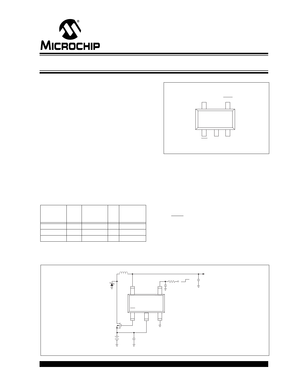
The TC105 is a step-down (Buck) switching controller
that furnishes output currents of up to 1A (max) while
delivering a typical efficiency of 92%. The TC105
normally operates in pulse width modulation mode
(PWM), but automatically switches to pulse frequency
modulation (PFM) at low output loads for greater
efficiency. Oscillator frequency is 300kHz, allowing use
of small (22
H) inductors. Supply current draw is only
102
A (max), and is reduced to less than 0.5A when
the SHDN input is brought low. Regulator operation is
suspended during shutdown. The TC105 accepts a
maximum input voltage of 10V.
The TC105 is available in a small 5-Pin SOT-23A
package, occupies minimum board space and is ideal
for a wide range of applications.
Functional Block Diagram
Part
Number
Output
Voltage
(V)*
Package
Osc.
Freq.
(kHz)
Operating
Temp.
Range
TC105503ECT
5.0
5-Pin SOT-23A
300
-40
C to +85C
TC105333ECT
3.3
5-Pin SOT-23A
300
-40
C to +85C
TC105303ECT
3.0
5-Pin SOT-23A
300
-40
C to +85C
TC105
1
2
3
5
4
V
DD
GND
5-Pin SOT-23A
NOTE: 5-Pin SOT-23A is equivalent to the EIAJ SC-74A
V
OUT
SHDN
EXT
(From System
Control Logic)
5
4
TC105333ECT
1
3
2
V
DD
EXT
GND
V
OUT
ON
OFF
SHDN
3.3V
V
OUT
L
1
22
µH (Sumida CD54)
D
1
MA737
Si 9430
P
V
BATT
6V
NiMH
C
1
10
µF/16V
R
SS
470K
C
SS
0.033
µF
C2
47
µF
10V
Tantalum
3.3V Regulated Supply Using 6V
NiMH Battery Pack Input
+
–
PFM/PWM Step-Down DC/DC Controller
TC105
DS21349C-page 2
2001-2012 Microchip Technology Inc.
1.0
ELECTRICAL
CHARACTERISTICS
Absolute Maximum Ratings*
Voltage on V
DD
....................................... -0.3V to +12V
EXT Output Current ........................................±100mA
Voltage on V
OUT
, EXT,
SHDN Pins .....................................-0.3V to V
DD
+0.3V
Power Dissipation.............................................150mW
Operating Temperature Range............. -40°C to +85°C
Storage Temperature Range ..............-40°C to +125°C
*Stresses above those listed under "Absolute Maximum
Ratings" may cause permanent damage to the device. These
are stress ratings only and functional operation of the device
at these or any other conditions above those indicated in the
operation sections of the specifications is not implied.
Exposure to Absolute Maximum Rating conditions for
extended periods may affect device reliability.
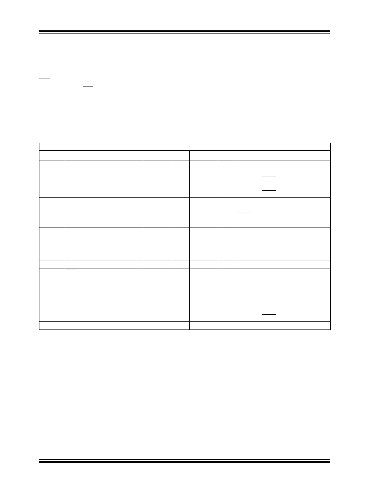
TC105 ELECTRICAL SPECIFICATIONS
Electrical Characteristics: Note 1, f
OSC
= 300 kHz; T
A
= 25°C, unless otherwise noted.
Symbol
Parameter
Min
Typ
Max
Units
Test Conditions
V
DD
Operating Supply Voltage
2.2
—
10.0
V
V
DD
MIN
Minimum Input Voltage
0.9
—
2.2
V
EXT = High; No external components;
V
OUT
= 0V, SHDN = V
IN
I
DD
Operating Supply Current
—
—
57
67
102
122
A
No external components; V
R
= 3.0V, 3.3V
V
OUT
= 0V, SHDN = V
IN
V
R
= 5.0V
I
STBY
Standby Supply Current
—
—
15
16
27
29
A
No external components; V
R
= 3.0V, 3.3V
V
OUT
= SHDN = V
IN
V
R
= 5.0V
I
SHDN
Shutdown Supply Current
—
—
0.5
A
SHDN = GND
f
OSC
Oscillator Frequency
255
300
345
kHz
V
IN
= V
OUT
+ 0.3V
V
OUT
Output Voltage
V
R
x 0.975
V
R
V
R
x 1.025
Note 2
DTYMAX Maximum Duty Cycle (PWM Mode)
100
—
—
%
DTYPFM
Duty Cycle (PFM Mode)
15
25
35
%
I
OUT
= 0mA
V
IH
SHDN Input Logic High
0.65
—
—
V
V
OUT
= 0V, No external components
V
IL
SHDN Input Logic Low
—
—
0.20
V
V
OUT
= 0V, No external components
REXTH
EXT ON Resistance to V
DD
—
—
—
17
16
12
24
22
17
No external components; V
R
= 3.0V
V
R
= 3.3V
V
R
= 5.0V
V
OUT
= SHDN = V
IN
, V
EXT
= (V
IN
– 0.4V)
REXTL
EXT ON Resistance to GND
—
—
—
15
14
10
20
19
14
No external components; V
R
= 3.0V
V
R
= 3.3V
V
R
= 5.0V
V
OUT
= 0V, SHDN = V
IN
, V
EXT
= 0.4V
Efficiency
—
92
—
%
Note
1:
V
R
= 3.0V, V
IN
= 4.5V, I
OUT
= 200mA
V
R
= 3.3V, V
IN
= 5.0V, I
OUT
= 220mA
V
R
= 5.0V, V
IN
= 7.5V, I
OUT
= 320mA
2:
V
R
is the factory output voltage setting.
2001-2012 Microchip Technology Inc.
DS21349C-page 3
TC105
2.0
PIN DESCRIPTIONS
The descriptions of the pins are listed in Table 2-1.
TABLE 2-1:
PIN FUNCTION TABLE
Pin No.
(5-Pin SOT-23A)
Symbol
Description
1
EXT
Switch transistor control output. This terminal connects to the gate of an external P-channel
MOSFET (or to the base of an external PNP transistor through a current limiting resistor).
2
V
DD
Power supply voltage input.
3
GND
Ground terminal.
4
SHDN
Shutdown input (active low). The device enters a low power shutdown state when this input is
brought low. During shutdown, regulator action is suspended, and supply current is reduced to
less than 0.5
A. The device resumes normal operation when SHDN is again brought high.
5
V
OUT
Voltage sense input. This input senses output voltage for regulation and must be connected to the
output voltage node as shown in the application schematic in this data sheet.

TC105
DS21349C-page 4
2001-2012 Microchip Technology Inc.
3.0
DETAILED DESCRIPTION
The TC105 is a PFM/PWM step-down DC/DC
controller for use in systems operating from two or
more cells, or in line-powered applications. It uses
PWM as the primary modulation scheme, but automat-
ically converts to PFM at output duty cycles less than
approximately 10%. The conversion to PFM provides
reduced supply current, and therefore higher operating
efficiency at low loads. The TC105 uses an external
switching transistor, allowing construction of switching
regulators with output currents of up to 1A.
The TC105 consumes only 102
A, max, of supply
current when V
IN
= 5V and V
OUT
= 3.3V, and can be
placed in a 0.5
A shutdown mode by bringing the
shutdown input (SHDN) low. The regulator remains
disabled while in shutdown mode, and output voltage
discharges to zero through the load. Normal operation
resumes when SHDN is brought high. Other features
include a built-in undervoltage lockout (UVLO) and
externally programmable soft start time.
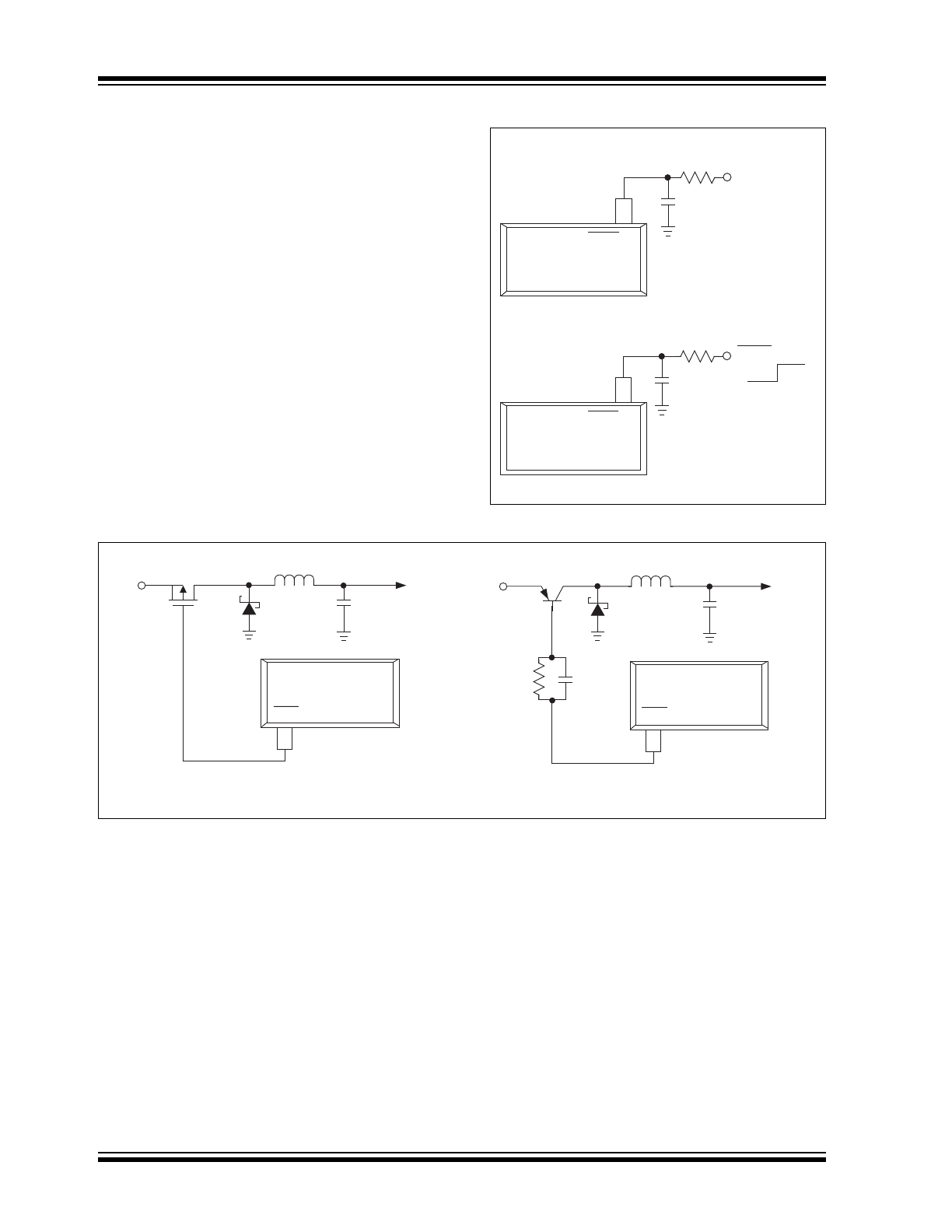
3.1
Low Power Shutdown Mode
The TC105 enters a low power shutdown mode when
SHDN is brought low. While in shutdown, the oscillator
is disabled and the output switch is shut off. Normal
regulator operation resumes when SHDN is again
brought high. SHDN may be tied to the input supply if
not used.
3.2
Soft Start
Soft start allows the output voltage to gradually ramp
from 0 to rated output value during start-up. This action
minimizes (or eliminates) overshoot, and in general,
reduces stress on circuit components. Figure 4-1
shows the circuit required to implement soft start
(values of 470K and 0.033
F for R
SS
and C
SS
respectively, are adequate for most applications).
3.3
Undervoltage Lockout (UVLO)
The TC105 is disabled when V
IN
is below the under-
voltage lockout threshold. This threshold is equal to the
guaranteed minimum operating voltage for the TC105
(i.e., 2.2V). When UVLO is active, the TC105 is
completely disabled.
3.4
Input Bypass Capacitors
Using an input bypass capacitor reduces peak current
transients drawn from the input supply and reduces the
switching noise generated by the regulator. The source
impedance of the input supply determines the size of
the capacitor that should be used.
3.5
Output Capacitor
The effective series resistance of the output capacitor
directly affects the amplitude of the output voltage
ripple. (The product of the peak inductor current and
the ESR determines output ripple amplitude.) There-
fore, a capacitor with the lowest possible ESR should
be selected. Smaller capacitors are acceptable for light
loads or in applications where ripple is not a concern.
The Sprague 595D series of tantalum capacitors are
among the smallest of all low ESR surface mount
capacitors available. Table 4-1 lists suggested
components and suppliers.
3.6
Inductor Selection
Selecting the proper inductor value is a trade-off
between physical size and power conversion require-
ments. Lower value inductors cost less, but result in
higher ripple current and core losses. They are also
more prone to saturate since the coil current ramps
faster and could overshoot the desired peak value. This
not only reduces efficiency, but could also cause the
current rating of the external components to be
exceeded. Larger inductor values reduce both ripple
current and core losses, but are larger in physical size
and tend to increase the start-up time slightly.
A 22
H inductor is recommended as the best overall
compromise. For highest efficiency, use inductors with
a low DC resistance (less than 20 m
). To minimize
radiated noise, consider using a toroid, pot core or
shielded-bobbin inductor.
3.7
Output Diode
The high operating frequency of the TC105 requires a
high-speed diode. Schottky diodes such as the MA737
or 1N5817 through 1N5823 (and the equivalent surface
mount versions) are recommended. Select a diode
whose average current rating is greater than the peak
inductor current and whose voltage rating is higher
than V
DD
MAX
.

2001-2012 Microchip Technology Inc.
DS21349C-page 5
TC105
3.8
External Switching Transistor
Selection
EXT is a complementary output with a maximum ON
resistance of 22
to V
DD
when high and 19
to ground
when low. It is designed to directly drive a P-channel
MOSFET or a PNP bipolar transistor through a base
current limiting resistor (Figure 4-2). A PNP transistor is
recommended in applications where V
IN
is less than
2.5V. Otherwise, a P-channel MOSFET is preferred as
it affords the highest efficiency because it does not
draw any gate drive current. However, P-channel
MOSFETs are typically more expensive than bipolar
transistors.
P-channel MOSFET selection is determined mainly by
the on-resistance, gate-source threshold, and gate
charge requirements. Also, the drain-to-source and
gate-to-source breakdown voltage ratings must be
greater than V
DD
MAX
. The total gate charge specifica-
tion should be less than 100nC for best efficiency. The
MOSFET must be capable of handling the required
peak inductor current, and should have a very low
on-resistance at that current. For example, an Si9430
MOSFET has a drain-to-source rating of -20V, and a
typical on-resistance r
DS
ON
of 0.07
at 2A, with V
GS
=
-4.5V. Table 4-1 lists suppliers of external components
recommended for use with the TC105.
3.8.1
BOARD LAYOUT GUIDELINES
As with all inductive switching regulators, the TC105
generates fast switching waveforms, which radiate
noise. Interconnecting lead lengths should be mini-
mized to keep stray capacitance, trace resistance and
radiated noise as low as possible. In addition, the GND
pin, input bypass capacitor and output filter capacitor
ground leads should be connected to a single point.
The input capacitor should be placed as close to power
and ground pins of the TC105 as possible. The length
of the EXT trace must also be kept as short as possible.
TC105
DS21349C-page 6
2001-2012 Microchip Technology Inc.
4.0
APPLICATIONS
4.1
Circuit Examples
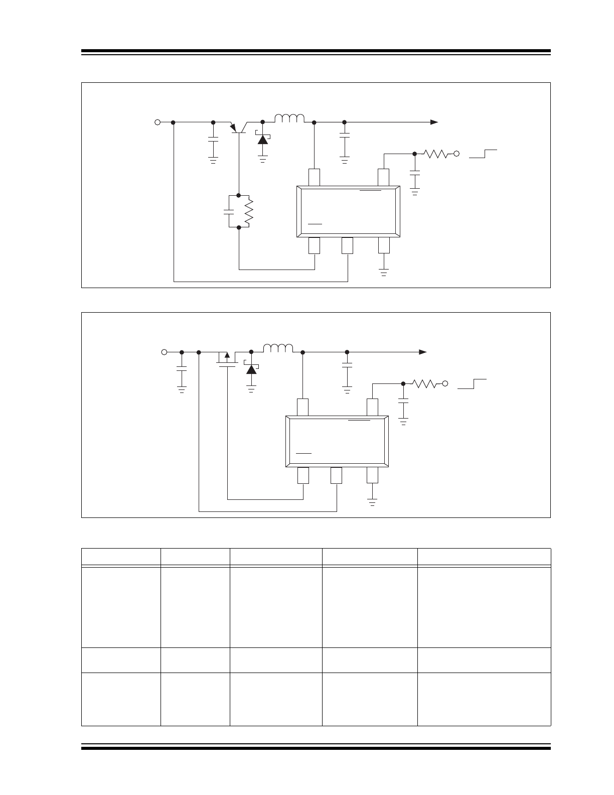
Figure 4-3 shows a TC105 using a PNP switching
transistor (Zetex FZT749) that has an h
FE
of 180 and
V
CESAT
of 100 mV at I
C
= 1A. Other high beta transis-
tors can be used, but the values of R
B
and C
B
may
need adjustment if h
FE
is significantly different from that
of the FZT749.
The circuit of Figure 4-4 utilizes a P-channel MOSFET
switching transistor (Silconix Si9430). This transistor is
a member of the Littlefoot™ family of small outline
MOSFETs.
FIGURE 4-1:
SOFT START CIRCUIT
FIGURE 4-2:
EXTERNAL TRANSISTOR CONNECTION
TC105
4
SHDN
SHDN/SS
TC105
4
V
IN
C
SS
0.033
µF
SHDN/SS
Shutdown Not Used
R
SS
470K
Shutdown Used
ON
OFF
(From System
Control Logic)
+
+
–
–
R
SS
470K
C
SS
0.033
µF
TC105
1
V
IN
V
OUT
Q
L
D
C
L
EXT
C
B
R
B
TC105
1
V
IN
V
OUT
P
L
D
EXT
C
L
P-Channel MOSFET
PNP Bipolar Transistor
–
+
–
+
–
+
2001-2012 Microchip Technology Inc.
DS21349C-page 7
TC105
FIGURE 4-3:
REGULATOR USING PNP TRANSISTOR
FIGURE 4-4:
REGULATOR USING P-CHANNEL MOSFET
TABLE 4-1:
SUGGESTED COMPONENTS AND SUPPLIERS
Type
Inductors
Capacitors
Diodes
Transistors
Surface Mount
Sumida
CD54 Series
CDRH Series
Coilcraft
DO Series
AVX
TPS Series
Sprague
595D Series
ON Semiconductor
MBRS340T3
Nihon
NSQ Series
Matsushita
MA737
Silconix
Little Foot MOSFET Series
Zetex FZT749
PNP Bipolar Transistor
Toshiba 2SA1213 PNP
Transistor
Miniature
Through-Hole
Sumida
RCH Series
Sanyo
OS-CON Series
IRC
OAR Series
Standard
Through-Hole
Coilcraft
PCH Series
Coiltronics
CTX Series
Nichicon
PL Series
United Chemi-Con
LXF Series
ON Semiconductor
TMOS Power MOSFETs
(i.e., MTP30P06V)
TC105
1
2
3
5
V
IN
2.5V
4
V
OUT
1.8V
ON
OFF
10
µ
F
16V
FZ749
Q1
22
µ
H
Sumida CD-54
MA737
47
µ
F
10V Tantalum
R
SS
470K
C
SS
0.033
µ
F
V
OUT
V
DD
EXT
GND
SHDN/SS
C
B
2200 pF
R
B
500
+
–
+
–
+
–
+
–
TC105
1
2
3
5
V
IN
4
V
OUT
ON
OFF
10
µ
F
16V
Si9430
P
22
µ
H
Sumida CD-54
MA737
47
µ
F
10V Tantalum
R
SS
470K
C
SS
0.033
µ
F
V
OUT
V
DD
EXT
GND
SHDN/SS
–
+
–
+
–
+
TC105
DS21349C-page 8
2001-2012 Microchip Technology Inc.
5.0
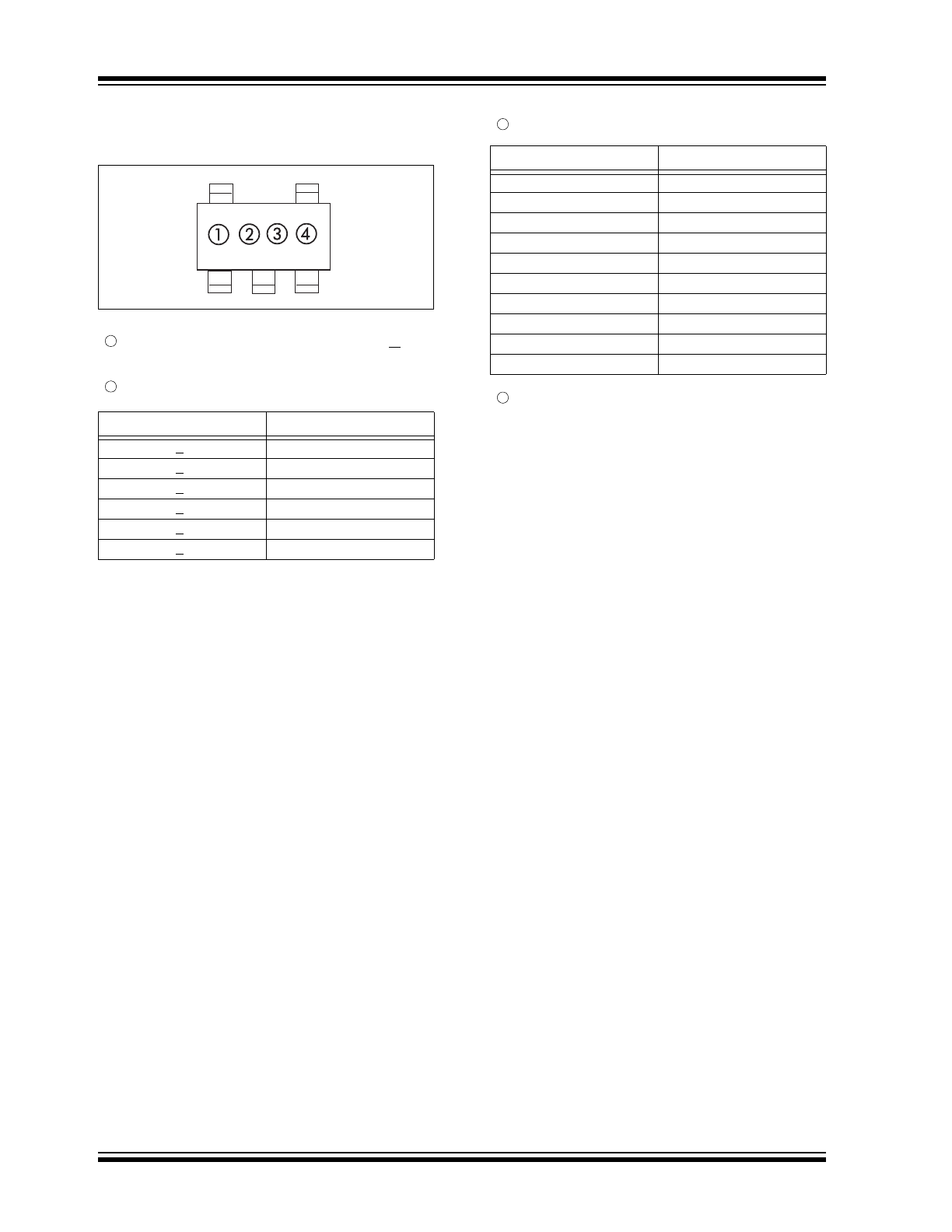
PACKAGING INFORMATION
5.1
Package Marking Information
Symbol (300kHz)
Voltage
1
1.
2
2.
3
3.
4
4.
5
5.
6
6.
1
represents product classification; TC105 = M
2
represents first integer of voltage
Symbol (300kHz)
Voltage
A
.0
B
.1
C
.2
D
.3
E
.4
F
.5
H
.6
K
.7
L
.8
M
.9
3
represents first decimal of voltage
4
represents production lot ID code
2001-2012 Microchip Technology Inc.
DS21349C-page 9
TC105
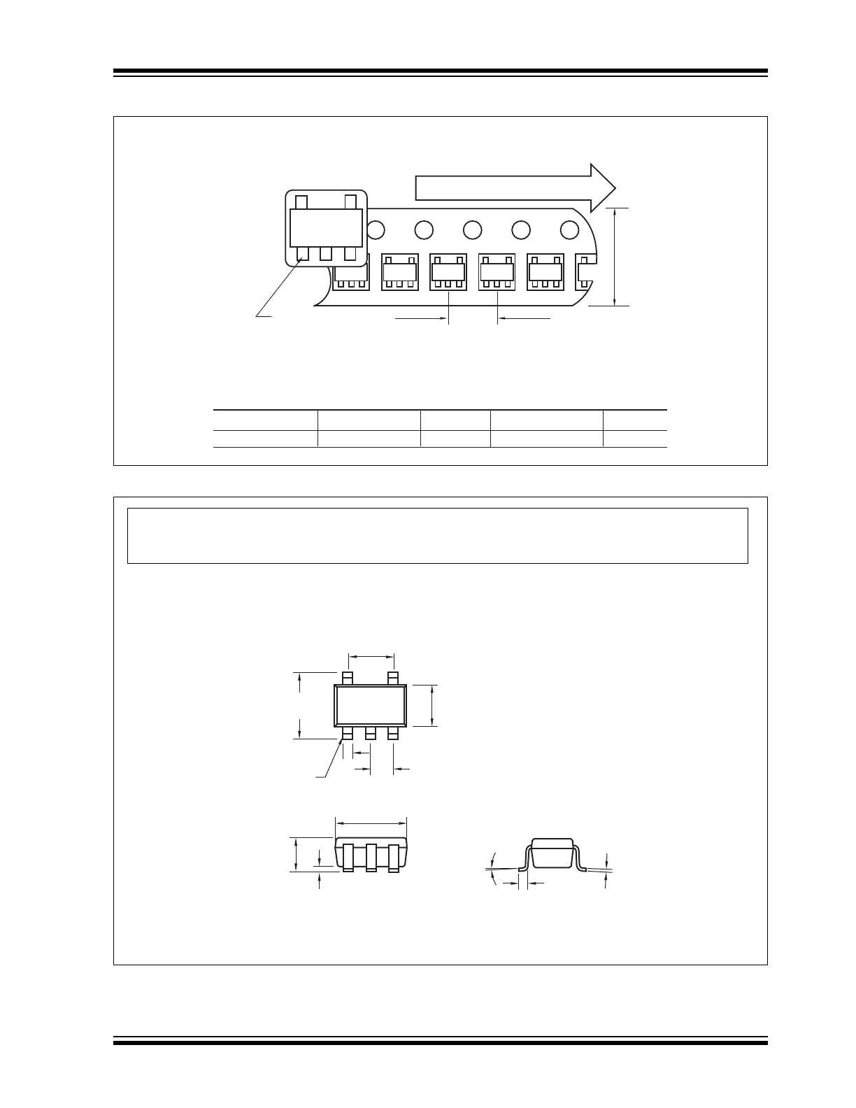
5.2
Taping Form
5.3
Package Dimensions
Component Taping Orientation for 5-Pin SOT-23A (EIAJ SC-74A) Devices
Package
Carrier Width (W)
Pitch (P)
Part Per Full Reel
Reel Size
5-Pin SOT-23A
8 mm
4 mm
3000
7 in
Carrier Tape, Number of Components Per Reel and Reel Size
User Direction of Feed
Device
Marking
PIN 1
Standard Reel Component Orientation
TR Suffix Device
(Mark Right Side Up)
W
P
.071 (1.80)
.059 (1.50)
.122 (3.10)
.098 (2.50)
.075 (1.90)
REF.
.020 (0.50)
.012 (0.30)
PIN 1
.037 (0.95)
REF.
.122 (3.10)
.106 (2.70)
.057 (1.45)
.035 (0.90)
.006 (0.15)
.000 (0.00)
.024 (0.60)
.004 (0.10)
10
°
MAX.
.010 (0.25)
.004 (0.09)
SOT-23A-5
Dimensions: inches (mm)
Note:
For the most current package drawings, please see the Microchip Packaging Specification located
at http://www.microchip.com/packaging

TC105
DS21349C-page 10
2001-2012 Microchip Technology Inc.
REVISION HISTORY
Revision C (November 2012)
Added a note to the package outline drawing.