
©
2005 Microchip Technology Inc.
DS21345C-page 1
Features
• Combines Two Comparators and a Voltage
Reference in a Single Package
• Optimized for Single Supply Operation
• Small Package: 8-Pin MSOP
• Ultra Low Input Bias Current: Less than 100pA
• Low Quiescent Current, Operating: 10
μ
A (Typ.)
Shutdown Mode: 6
μ
A (Typ.)
• Rail-to-Rail Inputs and Outputs
• Operates Down to V
DD
= 1.8V
• Reference and One Comparator Remain Active in
Shutdown to Provide Supervisory Functions
Applications
• Power Supply Circuits
• Battery Operated Equipment
• Consumer Products
• Replacements for Discrete Components
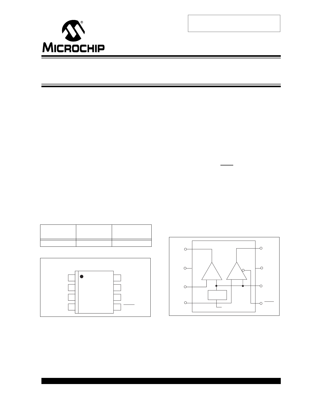
Device Selection Table
Package Type
General Description
The TC1040 is a mixed-function device combining two
comparators and a voltage reference in a single 8-pin
package. The inverting input of Comparator A and the
non-inverting input of Comparator B are internally
connected to the reference.
This increased integration allows the user to replace
two packages, which saves space, lowers supply
current and increases system performance. The
TC1040 operates from two 1.5V alkaline cells down to
V
DD
= 1.8V. It requires only 10
μ
A typical of supply
current, which significantly extends battery life. A low
power shutdown input (SHDN) disables one of the
comparators, placing its outputs in a high-impedance
state. This mode saves battery power and allows
comparator outputs to share common analog lines
(multiplexing). Shutdown current is 6
μ
A (typical).
Rail-to-rail inputs and outputs allow operation from low
supply voltages with large input and output signal
swings.
Packaged in an 8-Pin MSOP, the TC1040 is ideal for
applications requiring low power level detection.
Functional Block Diagram
Part Number
Package
Temperature
Range
TC1040CEUA
8-Pin MSOP
-40°C to +85°C
INB-
REF
1
2
3
4
8
7
6
5
TC1040CEUA
8-Pin MSOP
OUTB
V
DD
INA+
V
SS
OUTA
SHDN
+
–
+
–
TC1040
OUTB
V
DD
REF
SHDN
INB-
INA+
V
SS
OUTA
B
A
Voltage
Reference
V
SS
1
2
3
4
5
6
7
8
TC1040
Linear Building Block – Dual Low Power Comparator and
Voltage Reference with Shutdown
Obsolete Device
TC1040
DS21345C-page 2
©
2005 Microchip Technology Inc.
1.0
ELECTRICAL
CHARACTERISTICS
ABSOLUTE MAXIMUM RATINGS*
Supply Voltage ......................................................6.0V
Voltage on Any Pin .......... (V
SS
– 0.3V) to (V
DD
+ 0.3V)
Junction Temperature....................................... +150°C
Operating Temperature Range............. -40°C to +85°C
Storage Temperature Range ..............-55°C to +150°C
*Stresses above those listed under "Absolute Maximum
Ratings" may cause permanent damage to the device. These
are stress ratings only and functional operation of the device
at these or any other conditions above those indicated in the
operation sections of the specifications is not implied.
Exposure to Absolute Maximum Rating conditions for
extended periods may affect device reliability.
TC1040 ELECTRICAL SPECIFICATIONS
Electrical Characteristics: Typical values apply at 25°C and V
DD
= 3.0V. Minimum and maximum values apply for T
A
= -40° to
+85°C and V
DD
= 1.8V to 5.5V, unless otherwise specified.
Symbol
Parameter
Min
Typ
Max
Units
Test Conditions
V
DD
Supply Voltage
1.8
—
5.5
V
I
Q
Supply Current Operating
—
10
15
μ
A
All outputs unloaded, SHDN = V
DD
I
SHDN
Supply Current, Shutdown
—
0.05
0.1
μ
A
SHDN = V
SS
Shutdown Input
V
IH
Input High Threshold
80% V
DD
—
—
V
V
IL
Input Low Threshold
—
—
20% V
DD
V
I
SI
Shutdown Input Current
—
—
±100
nA
Comparators
R
OUT
(SD)
Output Resistance in Shutdown
20
—
—
M
Ω
SHDN = V
SS
, COMPB only
C
OUT
(SD)
Output Capacitance in Shutdown
—
—
5
pF
SHDN = V
SS
, COMPB only
T
SEL
Select Time (For Valid Output)
—
20
—
μ
sec
(SHDN = V
IH
to V
OUT
)
R
L
=10k
Ω
to V
SS,
COMPB only
T
DESEL
Deselect Time
—
500
—
nsec
(SHDN = V
IL
to V
OUT
)
R
L
=10k
Ω
to V
SS,
COMPB only
V
IR
Input Voltage Range
V
SS
– 0.2
—
V
DD
+ 0.2
V
V
OS
Input Offset Voltage
-5
-5
—
+5
+5
mV
V
DD
= 3V, T
A
= 25°C
T
A
= -40°C to 85°C
I
B
Input Bias Current
—
—
±100
pA
T
A
= 25°C, INA+, INB- = V
DD
to V
SS
V
OH
Output High Voltage
V
DD
– 0.3
—
—
V
R
L
= 10k
Ω
to V
SS
V
OL
Output Low Voltage
—
—
0.3
V
R
L
= 10k
Ω
to V
DD
PSRR
Power Supply Rejection Ratio
60
—
—
dB
T
A
= 25°C
V
DD
= 1.8V to 5V
I
SRC
Output Source Current
1
—
—
mA
INA+ = V
DD
, INB- = V
SS
Output Shorted to V
SS
V
DD
= 1.8V
I
SINK
Output Sink Current
2
—
—
mA
INA+ = V
SS
, INB- =V
DD,
Output Shorted to V
DD
V
DD
= 1.8V
t
PD1
Response Time
—
4
—
μ
sec
100mV Overdrive, C
L
= 100pF
t
PD2
Response Time
—
6
—
μ
sec
10mV Overdrive, C
L
= 100pF
Voltage Reference
V
REF
Reference Voltage
1.176
1.200
1.224
V
I
REF(SOURCE)
Source Current
50
—
—
μ
A
I
REF(SINK)
Sink Current
50
—
—
μ
A
C
L(REF)
Load Capacitance
—
—
100
pF
E
VREF
Voltage Noise
—
20
—
μ
V
RMS
100Hz to 100kHz
e
VREF
Noise Density
—
1.0
—
μ
V/
√
Hz 1kHz
©
2005 Microchip Technology Inc.
DS21345C-page 3
TC1040
2.0
PIN DESCRIPTION
The description of the pins are listed in Table 2-1.
TABLE 2-1:
PIN FUNCTION TABLE
Pin No.
(8-Pin MSOP)
Symbol
Description
1
OUTA
Comparator output.
2
V
SS
Negative power supply.
3
INA+
Non-inverting input to Comparator A.
4
INB-
Inverting input to Comparator B.
5
SHDN
Shutdown input.
6
REF
Voltage reference output.
7
V
DD
Positive power supply.
8
OUTB
Comparator output.
TC1040
DS21345C-page 4
©
2005 Microchip Technology Inc.
3.0
DETAILED DESCRIPTION
The TC1040 is one of a series of very low power, linear
building block products targeted at low voltage, single
supply applications. The TC1040 minimum operating
voltage is 1.8V and typical supply current is only 10
μ
A
(fully enabled). It combines two comparators and a
voltage reference in a single package. A shutdown
mode is incorporated for easy adaptation to system
power management schemes. During shutdown, one
comparator is disabled (i.e., powered down with output
at a high impedance). The “still awake” comparator and
voltage reference can be used as a wake-up timer,
power supply monitor, LDO controller or other
continuous duty circuit function.
3.1
Comparators
The TC1040 contains two comparators. The compara-
tor’s input range extends beyond both supply voltages
by 200mV and the outputs will swing to within several
millivolts of the supplies, depending on the load current
being driven. The inverting input of Comparator A and
the non-inverting input of Comparator B are internally
connected to the output of the voltage reference.
The comparators exhibit a propagation delay and
supply current which are largely independent of supply
voltage. The low input bias current and offset voltage
make them suitable for high impedance precision
applications.
Comparator B is disabled during shutdown and has a
high impedance output. Comparator COMPA remains
active.
3.2
Voltage Reference
A 2.0 percent tolerance, internally biased, 1.20V
bandgap voltage reference is included in the TC1040.
It has a push-pull output capable of sourcing and
sinking 50
μ
A. The voltage reference remains fully
enabled during shutdown.
3.3
Shutdown Input
SHDN at V
IL
disables one comparator. The SHDN input
cannot be allowed to float; when not used, connect it to
V
DD
. The disabled comparator’s output is in a high
impedance state when shutdown is active. The
disabled comparator’s inputs and outputs can be driven
from rail-to-rail by an external voltage when the
TC1040 is in shutdown. No latchup will occur when the
device is driven to its enabled state when SHDN is set
to V
IH
.
4.0
TYPICAL APPLICATIONS
The TC1040 lends itself to a wide variety of
applications, particularly in battery powered systems. It
typically finds application in power management,
processor supervisory and interface circuitry.
4.1
Wake-Up Timer
Many microcontrollers have a low-power “sleep” mode
that significantly reduces their supply current. Typically,
the microcontroller is placed in this mode via a software
instruction, and returns to a fully-enabled state upon
reception of an external signal (“wake-up”). The wake-
up signal is usually supplied by a hardware timer. Most
system applications demand that this timer have a long
duration (typically seconds or minutes), and consume
as little supply current as possible.
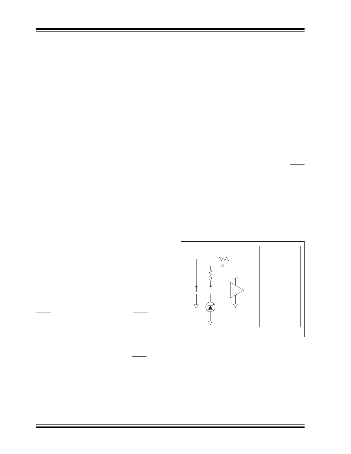
The circuit shown in Figure 4-1 is a wake-up timer
made from Comparator A. (Comparator A is used
because the wake-up timer must operate when SHDN
is active.) Capacitor C1 charges through R1 until a
voltage equal to V
R
is reached, at which point the
“wake-up” is driven active. Upon wake-up, the
microcontroller resets the timer by forcing a logic low
on a dedicated, open drain I/O port pin. This discharges
C1 through R4 (the value of R4 is chosen to limit
maximum current sunk by the I/O port pin). With a 3V
supply, the circuit as shown consumes typically 8
μ
A
and furnishes a nominal timer duration of 25 seconds.
FIGURE 4-1:
WAKE-UP TIMER
Wake-Up
R1
5M
R4
V
R
C
1
10
µF
V
DD
V
DD
–
+
I/O*
*Open Drain Port Pin
Microcontroller
COMPA
1/2
TC1040

©
2005 Microchip Technology Inc.
DS21345C-page 5
TC1040
4.2
Precision Battery Monitor
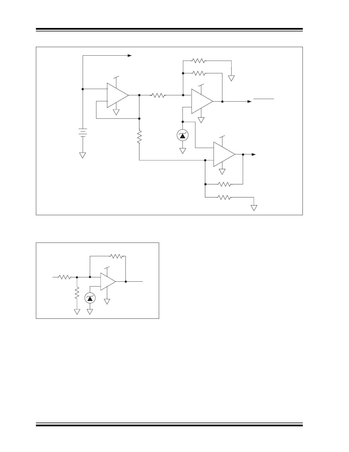
Figure 4-2 is a precision battery low/battery dead
monitoring circuit. Typically, the battery low output
warns the user that a battery dead condition is
imminent. Battery dead typically initiates a forced
shutdown to prevent operation at low internal supply
voltages (which can cause unstable system operation).
The circuit in Figure 4-2 uses a single TC1040, one-
half of a TC1029, and only six external resistors.
COMPA and COMPB provide precision voltage
detection using V
R
as a reference. Resistors R2 and
R4 set the detection threshold for BATT LOW, while
Resistors R1 and R7 set the detection threshold for
BATT FAIL. The component values shown assert
BATT LOW at 2.2V (typical) and BATT FAIL at 2.0
(typical). Total current consumed by this circuit is
typically 22
μ
A at 3V. Resistors R5 and R6 provide
hysteresis for comparators COMPA and COMPB,
respectively.
4.3
External Hysteresis (Comparator)
Hysteresis can be set externally with two resistors
using positive feedback techniques (see Figure 4-3).
The design procedure for setting external comparator
hysteresis is as follows:
1.
Choose the feedback resistor R
C
. Since the
input bias current of the comparator is at most
100pA, the current through R
C
can be set to
100nA (i.e., 1000 times the input bias current)
and retain excellent accuracy. The current
through R
C
at the comparator’s trip point is V
R
/
R
C
where V
R
is a stable reference voltage.
2.
Determine the hysteresis voltage (V
HY
) between
the upper and lower thresholds.
3.
Calculate R
A
as follows:
EQUATION 4-1:
4.
Choose the rising threshold voltage for V
SRC
(V
THR
).
5.
Calculate R
B
as follows:
EQUATION 4-2:
6.
Verify the threshold voltages with these
formulas:
V
SRC
rising:
EQUATION 4-3:
V
SRC
falling:
EQUATION 4-4:
R
A
R
C
V
HY
V
DD
-----------
⎝
⎠
⎛
⎞
=
R
B
1
V
THR
V
R
R
A
×
---------------------
⎝
⎛
⎠
⎞
1
R
A
-------
–
1
R
C
-------
–
-----------------------------------------------------------
=
V
THR
V
R
(
)
R
A
(
)
1
R
A
-------
⎝
⎠
⎛
⎞
1
R
B
-------
⎝
⎠
⎛
⎞
1
R
C
-------
⎝
⎠
⎛
⎞
+
+
=
V
THF
V
THR
R
A
V
DD
×
R
C
-------------------------
⎝
⎠
⎛
⎞
–
=
TC1040
DS21345C-page 6
©
2005 Microchip Technology Inc.
FIGURE 4-2:
PRECISION BATTERY MONITOR
FIGURE 4-3:
COMPARATOR
EXTERNAL HYSTERESIS
CONFIGURATION
V
DD
V
DD
V
DD
R2, 330k, 1%
R4, 470k, 1%
R5, 7.5M
R6, 7.5M
R3, 470k, 1%
R1, 270k, 1%
V
R
To System DC/DC
Converter
3V
Alkaline
TC1040
BATTFAIL
BATTLOW
COMPA
+
–
COMPB
+
–
AMP1
+
–
+
TC1034
+
–
V
R
V
DD
V
OUT
V
SRC
R
A
R
B
R
C
COMPA
TC1040
1/2
©
2005 Microchip Technology Inc.
DS21345C-page 7
TC1040
5.0
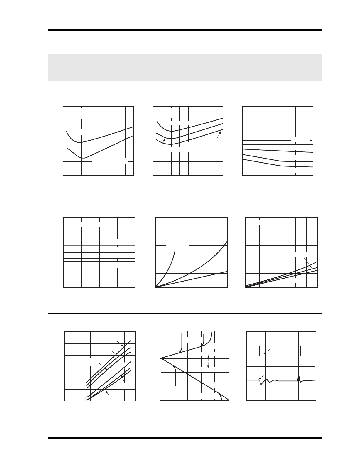
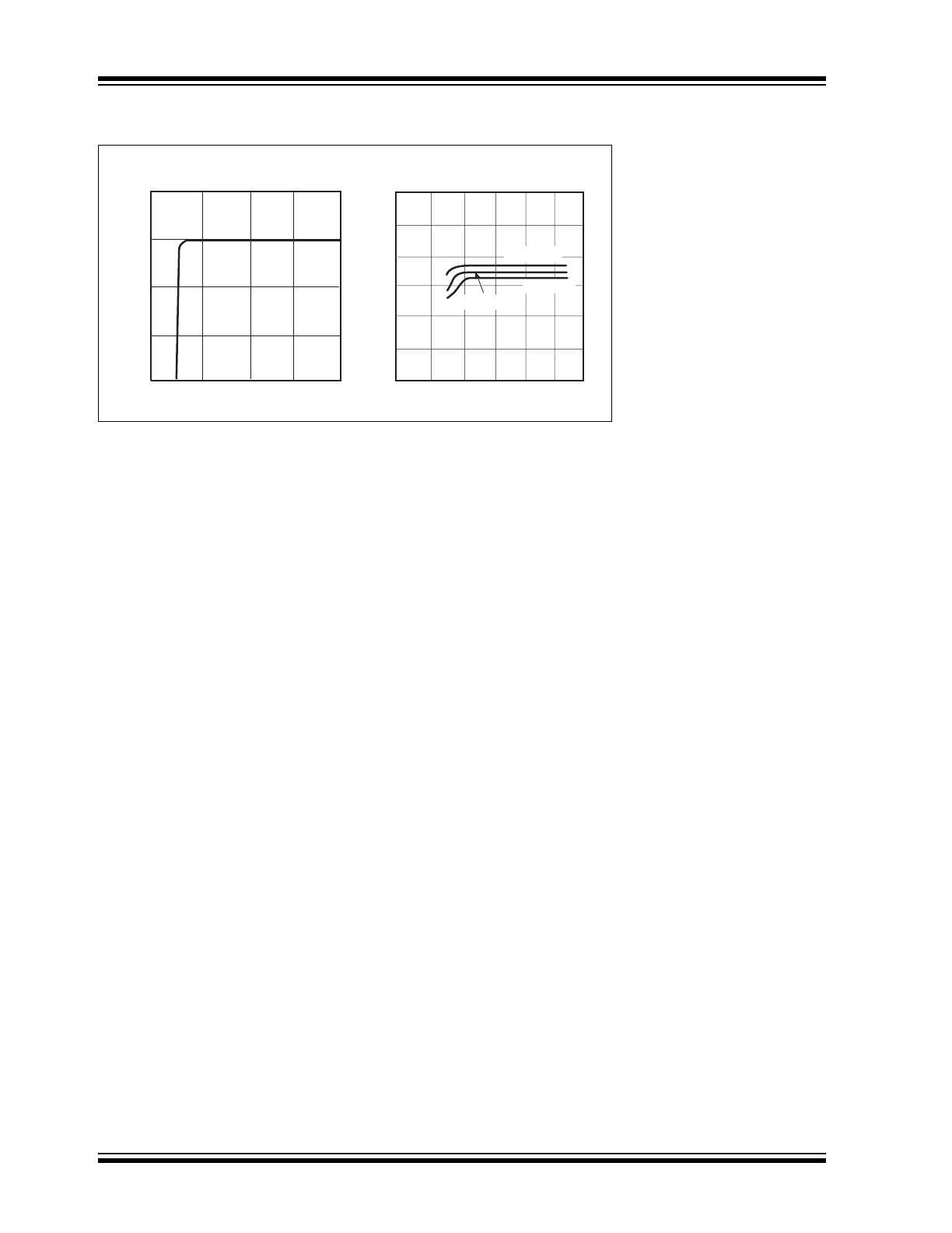
TYPICAL CHARACTERISTICS
Note:
The graphs and tables provided following this note are a statistical summary based on a limited number of
samples and are provided for informational purposes only. The performance characteristics listed herein
are not tested or guaranteed. In some graphs or tables, the data presented may be outside the specified
operating range (e.g., outside specified power supply range) and therefore outside the warranted range.
7
6
5
4
3
2
1.5
2
2.5
3
3.5
4
4.5
5
5.5
SUPPLY VOLTAGE (V)
SUPPLY VOLTAGE (V)
Comparator Propagation Delay
vs. Supply Voltage
DELAY TO RISING EDGE (
µ
sec)
Overdrive = 10mV
Overdrive = 50mV
7
6
5
4
3
2
1.5
2
2.5
3
3.5
4
4.5
5
5.5
DELAY TO FALLING EDGE (
µ
sec)
7
6
5
4
3
-40
°C
85
°C
25
°C
TEMPERATURE (
°C)
DELAY TO RISING EDGE (
µ
sec)
Overdrive = 100mV
Overdrive = 10mV
Overdrive = 50mV
Comparator Propagation Delay
vs. Supply Voltage
Comparator Propagation Delay
vs. Temperature
T
A
= 25°C
C
L
= 100pF
T
A
= 25°C
C
L
= 100pF
Overdrive = 100mV
V
DD
= 4V
V
DD
= 5V
V
DD
= 2V
V
DD
= 3V
-40
°C
85
°C
25
°C
2.5
2.0
1.5
1.0
.5
0
0
1
2
3
4
5
6
V
DD
- V
OUT
(V)
I
SOURCE
(mA)
7
6
5
4
3
Comparator Output Swing
vs. Output Source Current
DELAY TO FALLING EDGE (
µ
sec)
Overdrive = 100mV
2.5
2.0
1.5
1.0
.5
0
0
1
2
3
4
5
Comparator Propagation Delay
vs. Temperature
Comparator Output Swing
vs. Output Sink Current
TEMPERATURE (
°C)
I
SINK
(mA)
V
DD
= 4V
V
DD
= 5V
V
DD
= 2V
V
DD
= 3V
T
A
= 25°C
T
A
= 25°C
V
DD
= 3V
V
DD
= 1.8V
V
DD
= 5.5V
V
DD
= 3V
V
DD
= 1.8V
V
DD
= 5.5V
V
OUT
- V
SS
(V)
6
60
50
Sinking
40
30
20
10
0
0
1
2
3
4
5
6
OUTPUT SHORT-CIRCUIT CURRENT (mA)
SUPPLY VOLTAGE (V)
Comparator Output Short-Circuit
Current vs. Supply Voltage
Sourcing
T
A
= -40
°C
T
A
= -40
°C
T
A
= 25
°C
T
A
= 85
°C
T
A
= 25
°C
T
A
= 85
°C
REFERENCE VOLTAGE (V)
1.240
1.220
1.200
1.180
1.160
1.140
0
2
4
6
8
10
LOAD CURRENT (mA)
Reference Voltage vs.
Load Current
V
DD
= 1.8V
V
DD
= 3V
V
DD
= 5.5V
Sinking
Sourcing
V
DD
= 1.8V
V
DD
= 3V
V
DD
= 5.5V
4
3
2
1
0
0
100
200
300
400
SUPPLY AND REFERENCE VOLTAGES (V)
TIME (
µsec)
Line Transient
Response of V
REF
V
DD
V
REF
TC1040
DS21345C-page 8
©
2005 Microchip Technology Inc.
5.0 TYPICAL CHARACTERISTICS (CONTINUED)
1.25
1.20
1.15
1.10
1.05
1
2
3
4
5
REFERENCE VOLTAGE (V)
0
1
2
3
4
5
6
SUPPLY CURRENT
(µ
A)
SUPPLY VOLTAGE (V)
Supply Current vs. Supply Voltage
T
A
= 85
°C
T
A
= -40
°C
T
A
= 25
°C
Reference Voltage
vs. Supply Voltage
SUPPLY VOLTAGE (V)
12
11
10
9
8
7
6
©
2005 Microchip Technology Inc.
DS21345C-page 9
TC1040
6.0
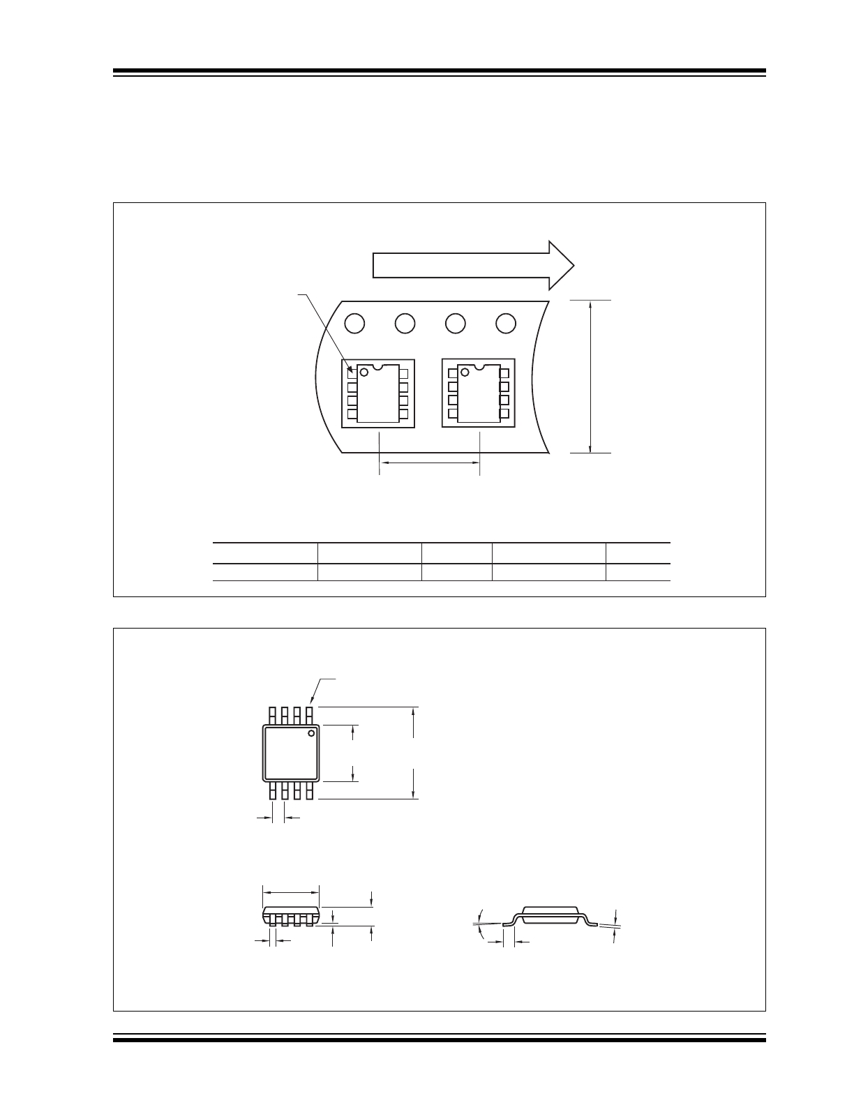
PACKAGING INFORMATION
6.1
Package Marking Information
Package marking data not available at this time.
6.2
Taping Form
6.3
Package Dimensions
Component Taping Orientation for 8-Pin MSOP Devices
Package
Carrier Width (W)
Pitch (P)
Part Per Full Reel
Reel Size
8-Pin MSOP
12 mm
8 mm
2500
13 in
Carrier Tape, Number of Components Per Reel and Reel Size
PIN 1
User Direction of Feed
Standard Reel Component Orientation
for TR Suffix Device
W
P
8-Pin MSOP
.122 (3.10)
.114 (2.90)
.122 (3.10)
.114 (2.90)
.043 (1.10)
MAX.
.006 (0.15)
.002 (0.05)
.016 (0.40)
.010 (0.25)
.197 (5.00)
.189 (4.80)
.008 (0.20)
.005 (0.13)
.028 (0.70)
.016 (0.40)
6
° MAX.
.026 (0.65) TYP.
PIN 1
Dimensions: inches (mm)

TC1040
DS21345C-page 10
©
2005 Microchip Technology Inc.
NOTES:
©
2005 Microchip Technology Inc.
DS21345C-page 1
Features
• Combines Two Comparators and a Voltage
Reference in a Single Package
• Optimized for Single Supply Operation
• Small Package: 8-Pin MSOP
• Ultra Low Input Bias Current: Less than 100pA
• Low Quiescent Current, Operating: 10
μ
A (Typ.)
Shutdown Mode: 6
μ
A (Typ.)
• Rail-to-Rail Inputs and Outputs
• Operates Down to V
DD
= 1.8V
• Reference and One Comparator Remain Active in
Shutdown to Provide Supervisory Functions
Applications
• Power Supply Circuits
• Battery Operated Equipment
• Consumer Products
• Replacements for Discrete Components
Device Selection Table
Package Type
General Description
The TC1040 is a mixed-function device combining two
comparators and a voltage reference in a single 8-pin
package. The inverting input of Comparator A and the
non-inverting input of Comparator B are internally
connected to the reference.
This increased integration allows the user to replace
two packages, which saves space, lowers supply
current and increases system performance. The
TC1040 operates from two 1.5V alkaline cells down to
V
DD
= 1.8V. It requires only 10
μ
A typical of supply
current, which significantly extends battery life. A low
power shutdown input (SHDN) disables one of the
comparators, placing its outputs in a high-impedance
state. This mode saves battery power and allows
comparator outputs to share common analog lines
(multiplexing). Shutdown current is 6
μ
A (typical).
Rail-to-rail inputs and outputs allow operation from low
supply voltages with large input and output signal
swings.
Packaged in an 8-Pin MSOP, the TC1040 is ideal for
applications requiring low power level detection.
Functional Block Diagram
Part Number
Package
Temperature
Range
TC1040CEUA
8-Pin MSOP
-40°C to +85°C
INB-
REF
1
2
3
4
8
7
6
5
TC1040CEUA
8-Pin MSOP
OUTB
V
DD
INA+
V
SS
OUTA
SHDN
+
–
+
–
TC1040
OUTB
V
DD
REF
SHDN
INB-
INA+
V
SS
OUTA
B
A
Voltage
Reference
V
SS
1
2
3
4
5
6
7
8
TC1040
Linear Building Block – Dual Low Power Comparator and
Voltage Reference with Shutdown
Obsolete Device
TC1040
DS21345C-page 2
©
2005 Microchip Technology Inc.
1.0
ELECTRICAL
CHARACTERISTICS
ABSOLUTE MAXIMUM RATINGS*
Supply Voltage ......................................................6.0V
Voltage on Any Pin .......... (V
SS
– 0.3V) to (V
DD
+ 0.3V)
Junction Temperature....................................... +150°C
Operating Temperature Range............. -40°C to +85°C
Storage Temperature Range ..............-55°C to +150°C
*Stresses above those listed under "Absolute Maximum
Ratings" may cause permanent damage to the device. These
are stress ratings only and functional operation of the device
at these or any other conditions above those indicated in the
operation sections of the specifications is not implied.
Exposure to Absolute Maximum Rating conditions for
extended periods may affect device reliability.
TC1040 ELECTRICAL SPECIFICATIONS
Electrical Characteristics: Typical values apply at 25°C and V
DD
= 3.0V. Minimum and maximum values apply for T
A
= -40° to
+85°C and V
DD
= 1.8V to 5.5V, unless otherwise specified.
Symbol
Parameter
Min
Typ
Max
Units
Test Conditions
V
DD
Supply Voltage
1.8
—
5.5
V
I
Q
Supply Current Operating
—
10
15
μ
A
All outputs unloaded, SHDN = V
DD
I
SHDN
Supply Current, Shutdown
—
0.05
0.1
μ
A
SHDN = V
SS
Shutdown Input
V
IH
Input High Threshold
80% V
DD
—
—
V
V
IL
Input Low Threshold
—
—
20% V
DD
V
I
SI
Shutdown Input Current
—
—
±100
nA
Comparators
R
OUT
(SD)
Output Resistance in Shutdown
20
—
—
M
Ω
SHDN = V
SS
, COMPB only
C
OUT
(SD)
Output Capacitance in Shutdown
—
—
5
pF
SHDN = V
SS
, COMPB only
T
SEL
Select Time (For Valid Output)
—
20
—
μ
sec
(SHDN = V
IH
to V
OUT
)
R
L
=10k
Ω
to V
SS,
COMPB only
T
DESEL
Deselect Time
—
500
—
nsec
(SHDN = V
IL
to V
OUT
)
R
L
=10k
Ω
to V
SS,
COMPB only
V
IR
Input Voltage Range
V
SS
– 0.2
—
V
DD
+ 0.2
V
V
OS
Input Offset Voltage
-5
-5
—
+5
+5
mV
V
DD
= 3V, T
A
= 25°C
T
A
= -40°C to 85°C
I
B
Input Bias Current
—
—
±100
pA
T
A
= 25°C, INA+, INB- = V
DD
to V
SS
V
OH
Output High Voltage
V
DD
– 0.3
—
—
V
R
L
= 10k
Ω
to V
SS
V
OL
Output Low Voltage
—
—
0.3
V
R
L
= 10k
Ω
to V
DD
PSRR
Power Supply Rejection Ratio
60
—
—
dB
T
A
= 25°C
V
DD
= 1.8V to 5V
I
SRC
Output Source Current
1
—
—
mA
INA+ = V
DD
, INB- = V
SS
Output Shorted to V
SS
V
DD
= 1.8V
I
SINK
Output Sink Current
2
—
—
mA
INA+ = V
SS
, INB- =V
DD,
Output Shorted to V
DD
V
DD
= 1.8V
t
PD1
Response Time
—
4
—
μ
sec
100mV Overdrive, C
L
= 100pF
t
PD2
Response Time
—
6
—
μ
sec
10mV Overdrive, C
L
= 100pF
Voltage Reference
V
REF
Reference Voltage
1.176
1.200
1.224
V
I
REF(SOURCE)
Source Current
50
—
—
μ
A
I
REF(SINK)
Sink Current
50
—
—
μ
A
C
L(REF)
Load Capacitance
—
—
100
pF
E
VREF
Voltage Noise
—
20
—
μ
V
RMS
100Hz to 100kHz
e
VREF
Noise Density
—
1.0
—
μ
V/
√
Hz 1kHz
©
2005 Microchip Technology Inc.
DS21345C-page 3
TC1040
2.0
PIN DESCRIPTION
The description of the pins are listed in Table 2-1.
TABLE 2-1:
PIN FUNCTION TABLE
Pin No.
(8-Pin MSOP)
Symbol
Description
1
OUTA
Comparator output.
2
V
SS
Negative power supply.
3
INA+
Non-inverting input to Comparator A.
4
INB-
Inverting input to Comparator B.
5
SHDN
Shutdown input.
6
REF
Voltage reference output.
7
V
DD
Positive power supply.
8
OUTB
Comparator output.
TC1040
DS21345C-page 4
©
2005 Microchip Technology Inc.
3.0
DETAILED DESCRIPTION
The TC1040 is one of a series of very low power, linear
building block products targeted at low voltage, single
supply applications. The TC1040 minimum operating
voltage is 1.8V and typical supply current is only 10
μ
A
(fully enabled). It combines two comparators and a
voltage reference in a single package. A shutdown
mode is incorporated for easy adaptation to system
power management schemes. During shutdown, one
comparator is disabled (i.e., powered down with output
at a high impedance). The “still awake” comparator and
voltage reference can be used as a wake-up timer,
power supply monitor, LDO controller or other
continuous duty circuit function.
3.1
Comparators
The TC1040 contains two comparators. The compara-
tor’s input range extends beyond both supply voltages
by 200mV and the outputs will swing to within several
millivolts of the supplies, depending on the load current
being driven. The inverting input of Comparator A and
the non-inverting input of Comparator B are internally
connected to the output of the voltage reference.
The comparators exhibit a propagation delay and
supply current which are largely independent of supply
voltage. The low input bias current and offset voltage
make them suitable for high impedance precision
applications.
Comparator B is disabled during shutdown and has a
high impedance output. Comparator COMPA remains
active.
3.2
Voltage Reference
A 2.0 percent tolerance, internally biased, 1.20V
bandgap voltage reference is included in the TC1040.
It has a push-pull output capable of sourcing and
sinking 50
μ
A. The voltage reference remains fully
enabled during shutdown.
3.3
Shutdown Input
SHDN at V
IL
disables one comparator. The SHDN input
cannot be allowed to float; when not used, connect it to
V
DD
. The disabled comparator’s output is in a high
impedance state when shutdown is active. The
disabled comparator’s inputs and outputs can be driven
from rail-to-rail by an external voltage when the
TC1040 is in shutdown. No latchup will occur when the
device is driven to its enabled state when SHDN is set
to V
IH
.
4.0
TYPICAL APPLICATIONS
The TC1040 lends itself to a wide variety of
applications, particularly in battery powered systems. It
typically finds application in power management,
processor supervisory and interface circuitry.
4.1
Wake-Up Timer
Many microcontrollers have a low-power “sleep” mode
that significantly reduces their supply current. Typically,
the microcontroller is placed in this mode via a software
instruction, and returns to a fully-enabled state upon
reception of an external signal (“wake-up”). The wake-
up signal is usually supplied by a hardware timer. Most
system applications demand that this timer have a long
duration (typically seconds or minutes), and consume
as little supply current as possible.
The circuit shown in Figure 4-1 is a wake-up timer
made from Comparator A. (Comparator A is used
because the wake-up timer must operate when SHDN
is active.) Capacitor C1 charges through R1 until a
voltage equal to V
R
is reached, at which point the
“wake-up” is driven active. Upon wake-up, the
microcontroller resets the timer by forcing a logic low
on a dedicated, open drain I/O port pin. This discharges
C1 through R4 (the value of R4 is chosen to limit
maximum current sunk by the I/O port pin). With a 3V
supply, the circuit as shown consumes typically 8
μ
A
and furnishes a nominal timer duration of 25 seconds.
FIGURE 4-1:
WAKE-UP TIMER
Wake-Up
R1
5M
R4
V
R
C
1
10
µF
V
DD
V
DD
–
+
I/O*
*Open Drain Port Pin
Microcontroller
COMPA
1/2
TC1040
©
2005 Microchip Technology Inc.
DS21345C-page 5
TC1040
4.2
Precision Battery Monitor
Figure 4-2 is a precision battery low/battery dead
monitoring circuit. Typically, the battery low output
warns the user that a battery dead condition is
imminent. Battery dead typically initiates a forced
shutdown to prevent operation at low internal supply
voltages (which can cause unstable system operation).
The circuit in Figure 4-2 uses a single TC1040, one-
half of a TC1029, and only six external resistors.
COMPA and COMPB provide precision voltage
detection using V
R
as a reference. Resistors R2 and
R4 set the detection threshold for BATT LOW, while
Resistors R1 and R7 set the detection threshold for
BATT FAIL. The component values shown assert
BATT LOW at 2.2V (typical) and BATT FAIL at 2.0
(typical). Total current consumed by this circuit is
typically 22
μ
A at 3V. Resistors R5 and R6 provide
hysteresis for comparators COMPA and COMPB,
respectively.
4.3
External Hysteresis (Comparator)
Hysteresis can be set externally with two resistors
using positive feedback techniques (see Figure 4-3).
The design procedure for setting external comparator
hysteresis is as follows:
1.
Choose the feedback resistor R
C
. Since the
input bias current of the comparator is at most
100pA, the current through R
C
can be set to
100nA (i.e., 1000 times the input bias current)
and retain excellent accuracy. The current
through R
C
at the comparator’s trip point is V
R
/
R
C
where V
R
is a stable reference voltage.
2.
Determine the hysteresis voltage (V
HY
) between
the upper and lower thresholds.
3.
Calculate R
A
as follows:
EQUATION 4-1:
4.
Choose the rising threshold voltage for V
SRC
(V
THR
).
5.
Calculate R
B
as follows:
EQUATION 4-2:
6.
Verify the threshold voltages with these
formulas:
V
SRC
rising:
EQUATION 4-3:
V
SRC
falling:
EQUATION 4-4:
R
A
R
C
V
HY
V
DD
-----------
⎝
⎠
⎛
⎞
=
R
B
1
V
THR
V
R
R
A
×
---------------------
⎝
⎛
⎠
⎞
1
R
A
-------
–
1
R
C
-------
–
-----------------------------------------------------------
=
V
THR
V
R
(
)
R
A
(
)
1
R
A
-------
⎝
⎠
⎛
⎞
1
R
B
-------
⎝
⎠
⎛
⎞
1
R
C
-------
⎝
⎠
⎛
⎞
+
+
=
V
THF
V
THR
R
A
V
DD
×
R
C
-------------------------
⎝
⎠
⎛
⎞
–
=
TC1040
DS21345C-page 6
©
2005 Microchip Technology Inc.
FIGURE 4-2:
PRECISION BATTERY MONITOR
FIGURE 4-3:
COMPARATOR
EXTERNAL HYSTERESIS
CONFIGURATION
V
DD
V
DD
V
DD
R2, 330k, 1%
R4, 470k, 1%
R5, 7.5M
R6, 7.5M
R3, 470k, 1%
R1, 270k, 1%
V
R
To System DC/DC
Converter
3V
Alkaline
TC1040
BATTFAIL
BATTLOW
COMPA
+
–
COMPB
+
–
AMP1
+
–
+
TC1034
+
–
V
R
V
DD
V
OUT
V
SRC
R
A
R
B
R
C
COMPA
TC1040
1/2
©
2005 Microchip Technology Inc.
DS21345C-page 7
TC1040
5.0
TYPICAL CHARACTERISTICS
Note:
The graphs and tables provided following this note are a statistical summary based on a limited number of
samples and are provided for informational purposes only. The performance characteristics listed herein
are not tested or guaranteed. In some graphs or tables, the data presented may be outside the specified
operating range (e.g., outside specified power supply range) and therefore outside the warranted range.
7
6
5
4
3
2
1.5
2
2.5
3
3.5
4
4.5
5
5.5
SUPPLY VOLTAGE (V)
SUPPLY VOLTAGE (V)
Comparator Propagation Delay
vs. Supply Voltage
DELAY TO RISING EDGE (
µ
sec)
Overdrive = 10mV
Overdrive = 50mV
7
6
5
4
3
2
1.5
2
2.5
3
3.5
4
4.5
5
5.5
DELAY TO FALLING EDGE (
µ
sec)
7
6
5
4
3
-40
°C
85
°C
25
°C
TEMPERATURE (
°C)
DELAY TO RISING EDGE (
µ
sec)
Overdrive = 100mV
Overdrive = 10mV
Overdrive = 50mV
Comparator Propagation Delay
vs. Supply Voltage
Comparator Propagation Delay
vs. Temperature
T
A
= 25°C
C
L
= 100pF
T
A
= 25°C
C
L
= 100pF
Overdrive = 100mV
V
DD
= 4V
V
DD
= 5V
V
DD
= 2V
V
DD
= 3V
-40
°C
85
°C
25
°C
2.5
2.0
1.5
1.0
.5
0
0
1
2
3
4
5
6
V
DD
- V
OUT
(V)
I
SOURCE
(mA)
7
6
5
4
3
Comparator Output Swing
vs. Output Source Current
DELAY TO FALLING EDGE (
µ
sec)
Overdrive = 100mV
2.5
2.0
1.5
1.0
.5
0
0
1
2
3
4
5
Comparator Propagation Delay
vs. Temperature
Comparator Output Swing
vs. Output Sink Current
TEMPERATURE (
°C)
I
SINK
(mA)
V
DD
= 4V
V
DD
= 5V
V
DD
= 2V
V
DD
= 3V
T
A
= 25°C
T
A
= 25°C
V
DD
= 3V
V
DD
= 1.8V
V
DD
= 5.5V
V
DD
= 3V
V
DD
= 1.8V
V
DD
= 5.5V
V
OUT
- V
SS
(V)
6
60
50
Sinking
40
30
20
10
0
0
1
2
3
4
5
6
OUTPUT SHORT-CIRCUIT CURRENT (mA)
SUPPLY VOLTAGE (V)
Comparator Output Short-Circuit
Current vs. Supply Voltage
Sourcing
T
A
= -40
°C
T
A
= -40
°C
T
A
= 25
°C
T
A
= 85
°C
T
A
= 25
°C
T
A
= 85
°C
REFERENCE VOLTAGE (V)
1.240
1.220
1.200
1.180
1.160
1.140
0
2
4
6
8
10
LOAD CURRENT (mA)
Reference Voltage vs.
Load Current
V
DD
= 1.8V
V
DD
= 3V
V
DD
= 5.5V
Sinking
Sourcing
V
DD
= 1.8V
V
DD
= 3V
V
DD
= 5.5V
4
3
2
1
0
0
100
200
300
400
SUPPLY AND REFERENCE VOLTAGES (V)
TIME (
µsec)
Line Transient
Response of V
REF
V
DD
V
REF
TC1040
DS21345C-page 8
©
2005 Microchip Technology Inc.
5.0 TYPICAL CHARACTERISTICS (CONTINUED)
1.25
1.20
1.15
1.10
1.05
1
2
3
4
5
REFERENCE VOLTAGE (V)
0
1
2
3
4
5
6
SUPPLY CURRENT
(µ
A)
SUPPLY VOLTAGE (V)
Supply Current vs. Supply Voltage
T
A
= 85
°C
T
A
= -40
°C
T
A
= 25
°C
Reference Voltage
vs. Supply Voltage
SUPPLY VOLTAGE (V)
12
11
10
9
8
7
6
©
2005 Microchip Technology Inc.
DS21345C-page 9
TC1040
6.0
PACKAGING INFORMATION
6.1
Package Marking Information
Package marking data not available at this time.
6.2
Taping Form
6.3
Package Dimensions
Component Taping Orientation for 8-Pin MSOP Devices
Package
Carrier Width (W)
Pitch (P)
Part Per Full Reel
Reel Size
8-Pin MSOP
12 mm
8 mm
2500
13 in
Carrier Tape, Number of Components Per Reel and Reel Size
PIN 1
User Direction of Feed
Standard Reel Component Orientation
for TR Suffix Device
W
P
8-Pin MSOP
.122 (3.10)
.114 (2.90)
.122 (3.10)
.114 (2.90)
.043 (1.10)
MAX.
.006 (0.15)
.002 (0.05)
.016 (0.40)
.010 (0.25)
.197 (5.00)
.189 (4.80)
.008 (0.20)
.005 (0.13)
.028 (0.70)
.016 (0.40)
6
° MAX.
.026 (0.65) TYP.
PIN 1
Dimensions: inches (mm)
TC1040
DS21345C-page 10
©
2005 Microchip Technology Inc.
NOTES: