
2003-2012 Microchip Technology Inc.
DS21333C-page 1
TC1302A/B
Features
• Dual Output LDO:
- V
OUT1
= 1.5V to 3.3V @ 300 mA
- V
OUT2
= 1.5V to 3.3V @ 150 mA
• Output Voltage (See Table 8-1)
• Low Dropout Voltage:
- V
OUT1
= 104 mV @ 300 mA Typical
- V
OUT2
= 150 mV @ 150 mA Typical
• Low Supply Current: 116 µA Typical
TC1302A/B with both output voltages available
• Reference Bypass Input for Low-Noise Operation
• Both Output Voltages Stable with a Minimum of
1 µF Ceramic Output Capacitor
• Separate V
OUT1
and V
OUT2
SHDN pins
(TC1302B)
• Power-Saving Shutdown Mode of Operation
• Wake-up from SHDN: 5.3 µs. Typical
• Small 8-pin DFN or MSOP Package Options
• Operating Junction Temperature Range:
- -40°C to +125°C
• Overtemperature and Overcurrent Protection
Applications
• Cellular/GSM/PHS Phones
• Battery-Operated Systems
• Hand-Held Medical Instruments
• Portable Computers/PDAs
• Linear Post-Regulators for SMPS
• Pagers
Related Literature
• AN765, “Using Microchip’s Micropower LDOs”,
DS00765, Microchip Technology Inc., 2002
• AN766, “Pin-Compatible CMOS Upgrades to
BiPolar LDOs”, DS00766,
Microchip Technology Inc., 2002
• AN792, “A Method to Determine How Much
Power a SOT23 Can Dissipate in an Application”,
DS00792, Microchip Technology Inc., 2001
Description
The TC1302A/B combines two Low Dropout (LDO)
regulators into a single 8-pin MSOP or DFN package.
Both regulator outputs feature low dropout voltage,
104 mV @ 300 mA for V
OUT1
, 150 mV @ 150 mA for
V
OUT2
, low quiescent current consumption, 58 µA each
and a typical regulation accuracy of 0.5%. Several
fixed-output voltage combinations are available. A
reference bypass pin is available to further reduce
output noise and improve the power supply rejection
ratio of both LDOs.
The TC1302A/B is stable over all line and load
conditions, with a minimum of 1 µF of ceramic output
capacitance, and utilizes a unique compensation
scheme to provide fast dynamic response to sudden
line voltage and load current changes.
Additional features include an overcurrent limit and
overtemperature protection that combine to provide a
robust design for all load fault conditions.
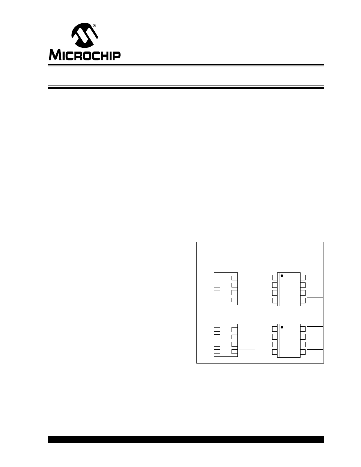
Package Types
8-Pin DFN/MSOP
NC
SHDN2
Bypass
GND
NC
1
2
3
4
5
6
7
8
V
OUT2
V
IN
1
2
3
4
5
6
7
8
V
OUT1
TC1302A
NC
SHDN2
Bypass
GND
NC
V
OUT2
V
IN
V
OUT1
DFN8
MSOP8
NC
SHDN2
Bypass
GND
SHDN1
1
2
3
4
5
6
7
8
V
OUT2
V
IN
1
2
3
4
5
6
7
8
V
OUT1
TC1302B
NC
SHDN2
Bypass
GND
SHDN1
V
OUT2
V
IN
V
OUT1
DFN8
MSOP8
Low Quiescent Current Dual Output LDO
TC1302A/B
DS21333C-page 2
2003-2012 Microchip Technology Inc.
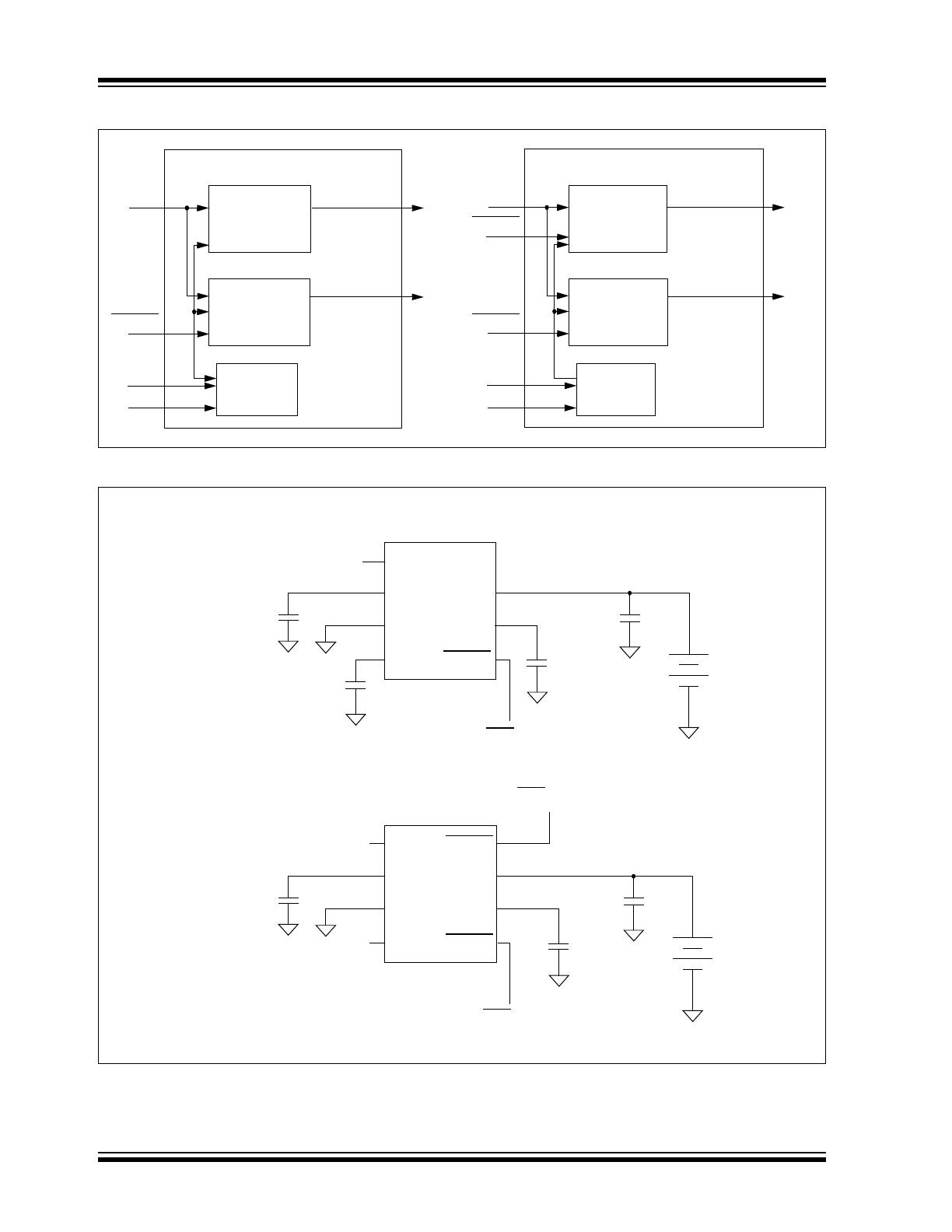
Functional Block Diagrams
Typical Application Circuits
LDO #2
150 mA
LDO #1
300 mA
LDO #2
150 mA
V
IN
V
OUT1
V
OUT2
Bandgap
Reference
SHDN2
GND
Bypass
TC1302A
TC1302B
V
IN
SHDN2
GND
Bypass
SHDN1
LDO #1
300 mA
Bandgap
Reference
V
OUT1
V
OUT2
1.2V
1.2V
8
4
1
2
3
NC
GND
NC
BATTERY
C
OUT1
1 µF Ceramic
X5R
C
IN
1 µF
TC1302A
C
OUT2
1 µF Ceramic
X5R
C
BYPASS
(Note)
10 nF Ceramic
Bypass
V
IN
7
2.7V
to
4.2V
V
OUT2
6
SHDN2
ON/OFF Control V
OUT2
2.8V @ 300 mA
2.6V @ 150 mA
5
V
OUT1
8
4
1
2
3
NC
GND
SHDN1
BATTERY
C
OUT1
1 µF Ceramic
X5R
C
IN
1 µF
TC1302B
C
OUT2
1 µF Ceramic
X5R
Bypass
V
IN
7
2.7V
to
4.2V
V
OUT2
6
SHDN2
ON/OFF Control V
OUT2
2.8V @ 300 mA
2.6V @ 150 mA
5
ON/OFF Control V
OUT1
Note: C
BYPASS
is optional
V
OUT1
2003-2012 Microchip Technology Inc.
DS21333C-page 3
TC1302A/B
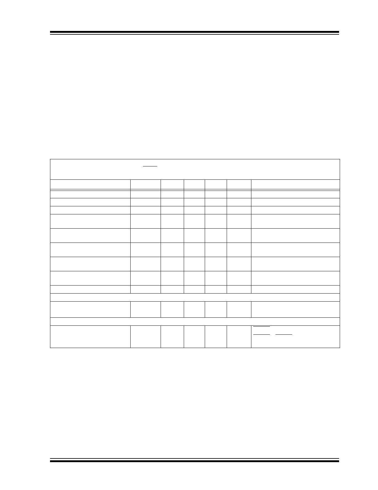
1.0
ELECTRICAL
CHARACTERISTICS
Absolute Maximum Ratings †
V
DD
...................................................................................6.5V
Maximum Voltage on Any Pin ...... (V
SS
– 0.3) to (V
IN
+ 0.3)V
Power Dissipation ..........................Internally Limited (Note 7)
Storage temperature .....................................-65°C to +150°C
Maximum Junction Temperature, T
J
........................... +150°C
Continuous Operating Temperature Range ..-40°C to +125°C
ESD protection on all pins, HBM, MM
4 kV, 400V
† Notice: Stresses above those listed under “Maximum Rat-
ings” may cause permanent damage to the device. This is a
stress rating only and functional operation of the device at
those or any other conditions above those indicated in the
operational listings of this specification is not implied. Expo-
sure to maximum rating conditions for extended periods may
affect device reliability.
DC CHARACTERISTICS
Electrical Specifications: Unless otherwise noted, V
IN
= V
R
+1V, I
OUT1
=
I
OUT2
= 100 µA, C
IN
= 4.7 µF,
C
OUT1
= C
OUT2
= 1 µF, C
BYPASS
= 10 nF, SHDN > V
IH
, T
A
= +25°C.
Boldface type specifications apply for junction temperatures of -40°C to +125°C.
Parameters
Sym
Min
Typ
Max
Units
Conditions
Input Operating Voltage
V
IN
2.7
—
6.0
V
Note 1
Maximum Output Current
I
OUT1Max
300
—
—
mA
V
IN
= 2.7V to 6.0V (Note 1)
Maximum Output Current
I
OUT2Max
150
—
—
mA
V
IN
= 2.7V to 6.0V (Note 1)
Output Voltage Tolerance
(V
OUT1
and V
OUT2
)
V
OUT
V
R
– 2.5
V
R
±0.5 V
R
+ 2.5
%
Note 2
Temperature Coefficient
(V
OUT1
and V
OUT2
)
TCV
OUT
—
25
—
ppm/°C
Note 3
Line Regulation
(V
OUT1
and V
OUT2
)
V
OUT
/
V
IN
—
0.02
0.2
%/V
(V
R
+ 1V)
V
IN
6V
Load Regulation, V
OUT
2.5V
(V
OUT1
and V
OUT2
)
V
OUT
V
OUT
-1
0.1
+1
%
I
OUTX
= 0.1 mA to I
OUTMax
,
(Note 4)
Load Regulation, V
OUT
< 2.5V
(V
OUT1
and V
OUT2
)
V
OUT
V
OUT
-1.5
0.1
+1.5
%
I
OUTX
= 0.1 mA to I
OUTMax
,
(Note 4)
Thermal Regulation
V
OUT
/
P
D
—
0.04
—
%/W
Note 5
Dropout Voltage (Note 6)
V
OUT1
> 2.7V
V
IN
– V
OUT
—
104
180
mV
I
OUT1
= 300 mA
V
OUT2
> 2.6V
V
IN
– V
OUT
—
150
250
mV
I
OUT2
= 150 mA
Supply Current
TC1302A
I
IN(A)
—
103
180
µA
SHDN2 = V
IN
, I
OUT1
= I
OUT2
= 0 mA
TC1302B
I
IN(B)
—
114
180
µA
SHDN1 = SHDN2 = V
IN
,
I
OUT1
= I
OUT2
= 0 mA
Note
1:
The minimum V
IN
has to meet two conditions: V
IN
2.7V and V
IN
V
R
+ V
DROPOUT
.
2:
V
R
is defined as the higher of the two regulator nominal output voltages (V
OUT1
or V
OUT2
).
3:
TCV
OUT
= ((V
OUTmax
- V
OUTmin
) * 10
6
)/(V
OUT
*
T).
4:
Regulation is measured at a constant junction temperature using low duty-cycle pulse testing. Load regulation is tested
over a load range from 0.1 mA to the maximum specified output current. Changes in output voltage due to heating
effects are covered by the thermal regulation specification.
5:
Thermal regulation is defined as the change in output voltage at a time t after a change in power dissipation is applied,
excluding load or line regulation effects. Specifications are for a current pulse equal to I
LMAX
at V
IN
= 6V for t = 10 msec.
6:
Dropout voltage is defined as the input-to-output voltage differential at which the output voltage drops 2% below its
value measured at a 1V differential.
7:
The maximum allowable power dissipation is a function of ambient temperature, the maximum allowable junction
temperature and the thermal resistance from junction to air (i.e., T
A
, T
J
,
JA
). Exceeding the maximum allowable power
dissipation causes the device to initiate thermal shutdown.
TC1302A/B
DS21333C-page 4
2003-2012 Microchip Technology Inc.
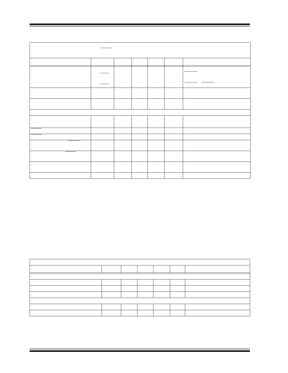
TEMPERATURE SPECIFICATIONS
Shutdown Supply Current
TC1302A
I
IN_SHDNA
—
58
90
µA
SHDN2 = GND
Shutdown Supply Current
TC1302B
I
IN_SHDNB
—
0.1
1
µA
SHDN1 = SHDN2 = GND
Power Supply Rejection Ratio
PSRR
—
58
—
dB
f
100 Hz, I
OUT1
= I
OUT2
= 50 mA,
C
IN
= 0 µF
Output Noise
eN
—
830
—
nV/(Hz)
½
f
1 kHz, I
OUT1
= I
OUT2
= 50 mA,
C
IN
= 0 µF
Output Short Circuit Current (Average)
V
OUT1
I
OUTsc1
—
200
—
mA
R
LOAD1
1
V
OUT2
I
OUTsc2
—
140
—
mA
R
LOAD2
1
SHDN Input High Threshold
V
IH
45
—
—
%V
IN
V
IN
= 2.7V to 6.0V
SHDN Input Low Threshold
V
IL
—
—
15
%V
IN
V
IN
= 2.7V to 6.0V
Wake Up Time (From SHDN
mode), (V
OUT2
)
t
WK
—
5.3
20
µs
V
IN
= 5V, I
OUT1
= I
OUT2
= 30 mA,
See Figure 5-1
Settling Time (From SHDN mode),
(V
OUT2
)
t
S
—
50
—
µs
V
IN
= 5V, I
OUT1
= I
OUT2
= 50 mA,
See Figure 5-2
Thermal Shutdown Die
Temperature
T
SD
—
150
—
°C
V
IN
= 5V, I
OUT1
= I
OUT2
= 100 µA
Thermal Shutdown Hysteresis
T
HYS
—
10
—
°C
V
IN
= 5V
Electrical Specifications: Unless otherwise indicated, all limits are specified for: V
IN
= +2.7V to +6.0V.
Parameters
Sym
Min
Typ
Max
Units
Conditions
Temperature Ranges
Operating Junction Temperature Range
T
A
-40
—
+125
°C
Steady State
Storage Temperature Range
T
A
-65
—
+150
°C
Maximum Junction Temperature
T
J
—
—
+150
°C
Transient
Thermal Package Resistances
Thermal Resistance, MSOP8
JA
—
208
—
°C/W
Typical 4-Layer Board
Thermal Resistance, DFN8
JA
—
41
—
°C/W
Typical 4-Layer Board with Vias
DC CHARACTERISTICS (Continued)
Electrical Specifications: Unless otherwise noted, V
IN
= V
R
+1V, I
OUT1
=
I
OUT2
= 100 µA, C
IN
= 4.7 µF,
C
OUT1
= C
OUT2
= 1 µF, C
BYPASS
= 10 nF, SHDN > V
IH
, T
A
= +25°C.
Boldface type specifications apply for junction temperatures of -40°C to +125°C.
Parameters
Sym
Min
Typ
Max
Units
Conditions
Note
1:
The minimum V
IN
has to meet two conditions: V
IN
2.7V and V
IN
V
R
+ V
DROPOUT
.
2:
V
R
is defined as the higher of the two regulator nominal output voltages (V
OUT1
or V
OUT2
).
3:
TCV
OUT
= ((V
OUTmax
- V
OUTmin
) * 10
6
)/(V
OUT
*
T).
4:
Regulation is measured at a constant junction temperature using low duty-cycle pulse testing. Load regulation is tested
over a load range from 0.1 mA to the maximum specified output current. Changes in output voltage due to heating
effects are covered by the thermal regulation specification.
5:
Thermal regulation is defined as the change in output voltage at a time t after a change in power dissipation is applied,
excluding load or line regulation effects. Specifications are for a current pulse equal to I
LMAX
at V
IN
= 6V for t = 10 msec.
6:
Dropout voltage is defined as the input-to-output voltage differential at which the output voltage drops 2% below its
value measured at a 1V differential.
7:
The maximum allowable power dissipation is a function of ambient temperature, the maximum allowable junction
temperature and the thermal resistance from junction to air (i.e., T
A
, T
J
,
JA
). Exceeding the maximum allowable power
dissipation causes the device to initiate thermal shutdown.
2003-2012 Microchip Technology Inc.
DS21333C-page 5
TC1302A/B
2.0
TYPICAL PERFORMANCE CURVES
Note: Unless otherwise indicated,
V
IN
= V
R
+1V, I
OUT1
=
I
OUT2
= 100 µA, C
IN
= 4.7 µF, C
OUT1 =
C
OUT2
= 1 µF (X5R or X7R),
C
BYPASS
= 0 pF, SHDN1 = SHDN2 > V
IH
, T
A
= +25°C.
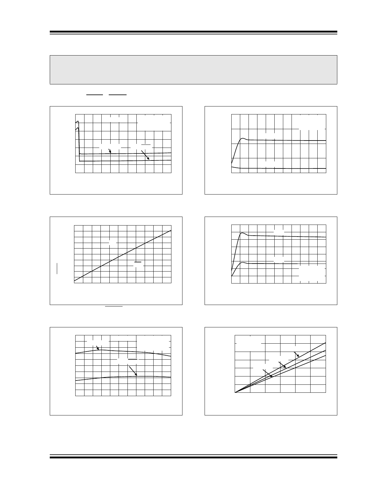
FIGURE 2-1:
Quiescent Current vs. Input
Voltage.
FIGURE 2-2:
SHDN Voltage Threshold
vs. Input Voltage.
FIGURE 2-3:
Quiescent Current vs.
Junction Temperature.
FIGURE 2-4:
Output Voltage vs. Input
Voltage.
FIGURE 2-5:
Output Voltage vs. Input
Voltage.
FIGURE 2-6:
Dropout Voltage vs. Output
Current (V
OUT1
).
Note:
The graphs and tables provided following this note are a statistical summary based on a limited number of
samples and are provided for informational purposes only. The performance characteristics listed herein
are not tested or guaranteed. In some graphs or tables, the data presented may be outside the specified
operating range (e.g., outside specified power supply range) and therefore outside the warranted range.
0
50
100
150
200
250
300
350
2.7 3.0 3.3 3.6 3.9 4.2 4.5 4.8 5.1 5.4 5.7 6.0
Input Voltage (V)
Quiescent C
u
rr
e
nt (µA
)
V
OUT2
SHDN
V
OUT2
Active
T
J
= +25°C
I
OUT1
= I
OUT2
= 0 µA
V
OUT1
Active
TC1302B
0.8
0.9
1.0
1.1
1.2
1.3
1.4
1.5
1.6
1.7
1.8
2.7
3
3.3 3.6 3.9 4.2 4.5 4.8 5.1 5.4 5.7
6
Input Voltage (V)
SH
D
N
Thr
e
s
hol
d
(V
)
ON
OFF
40
50
60
70
80
90
100
110
120
130
140
-40 -25 -10
5
20 35 50 65
80 95 110 125
Junction Temperature (°C)
Quiescent C
u
rr
e
nt (µA
)
V
IN
= 4.2V
I
OUT1
= I
OUT2
= 0 µA
V
OUT1
Active
V
OUT2
SHDN
V
OUT2
Active
TC1302B
2.60
2.70
2.80
2.90
3.00
2.7
3
3.3 3.6 3.9 4.2 4.5 4.8 5.1 5.4 5.7
6
Input Voltage (V)
Output V
o
ltage (V
)
T
J
= +25°C
I
OUT1
= 100 mA
I
OUT2
= 50 mA
V
OUT1
V
OUT2
2.50
2.55
2.60
2.65
2.70
2.75
2.80
2.85
2.90
2.7
3
3.3 3.6 3.9 4.2 4.5 4.8 5.1 5.4 5.7
6
Input Voltage (V)
Output V
o
ltage (V
)
T
J
= +25°C
I
OUT1
= 300 mA
I
OUT2
= 100 mA
V
OUT1
V
OUT2
0.0
20.0
40.0
60.0
80.0
100.0
120.0
140.0
0
50
100
150
200
250
300
I
OUT1
(mA)
D
ropout V
o
lt
age V
OUT
1
(m
V
)
V
R1
= 2.8V
V
R2
= 2.6V
I
OUT2
= 100 µA
T
J
= - 40°C
T
J
= +25°C
T
J
= +125°C
TC1302A/B
DS21333C-page 6
2003-2012 Microchip Technology Inc.
Note: Unless otherwise indicated,
V
IN
= V
R
+1V, I
OUT1
=
I
OUT2
= 100 µA, C
IN
= 4.7 µF, C
OUT1 =
C
OUT2
= 1 µF (X5R or X7R),
C
BYPASS
= 0 pF, SHDN1 = SHDN2 > V
IH
, T
A
= +25°C.
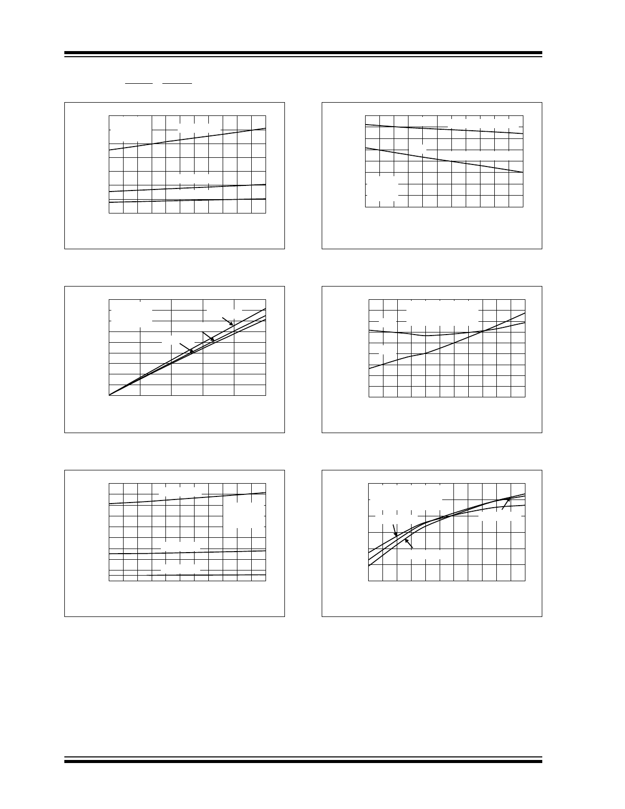
FIGURE 2-7:
Dropout Voltage vs.
Junction Temperature (V
OUT1
).
FIGURE 2-8:
Dropout Voltage vs. Output
Current (V
OUT2
).
FIGURE 2-9:
Dropout Voltage vs.
Junction Temperature (V
OUT2
).
FIGURE 2-10:
V
OUT1
and V
OUT2
Load
Regulation vs. Junction Temperature.
FIGURE 2-11:
V
OUT1
and V
OUT2
Line
Regulation vs. Junction Temperature.
FIGURE 2-12:
V
OUT1
vs. Junction
Temperature.
0
20
40
60
80
100
120
140
-40 -25 -10
5
20 35 50 65 80 95 110 125
Junction Temperature (°C)
D
ropout V
o
lt
age V
OUT
1
(m
V
)
V
R1
= 2.8V
V
R2
= 2.6V
I
OUT2
= 100 µA
I
OUT1
= 300 mA
I
OUT1
= 100 mA
I
OUT1
= 50 mA
0
20
40
60
80
100
120
140
160
180
0
30
60
90
120
150
I
OUT2
(mA)
D
ropout V
o
lt
age,
V
OUT
2
(m
v)
V
R1
= 2.8V
V
R2
= 2.6V
I
OUT1
= 100 µA
T
J
= +125°C
T
J
= +25°C
T
J
= - 40°C
0
20
40
60
80
100
120
140
160
180
-40 -25 -10
5
20 35 50 65 80 95 110 125
Junction Temperature (°C)
D
ropout V
o
lt
age V
OUT
2
(m
V
)
V
R1
= 2.8V
V
R2
= 2.6V
I
OUT1
= 100 µA
I
OUT2
= 150 mA
I
OUT2
= 50 mA
I
OUT2
= 10 mA
-0.40
-0.30
-0.20
-0.10
0.00
0.10
0.20
0.30
0.40
-40 -25 -10
5
20
35
50
65
80
95 110 125
Junction Temperature (125°C)
Load Regulation (%
)
I
OUT2
= 0.1 mA to 150 mA
I
OUT1
= 0.1 mA to 300 mA
V
R1
= 2.8V
V
R2
= 2.6V
V
IN
= 4.2
V
OUT2
V
OUT1
0.000
0.005
0.010
0.015
0.020
0.025
0.030
0.035
0.040
0.045
-40 -25 -10
5
20 35 50 65 80 95 110 125
Junction Temperature (°C)
Li
ne R
e
gul
ati
on (%
/V
)
V
IN
= 3.8V to 6.0V
V
R1
= 2.8V, I
OUT1
= 100 µA
V
R2
= 2.6V, I
OUT2
= 100 µA
V
OUT1
V
OUT2
2.808
2.812
2.816
2.820
2.824
2.828
2.832
-40 -25 -10
5
20 35 50 65 80 95 110 125
Junction Temperature (°C)
Ou
tp
u
t Vo
lt
ag
e V
OU
T1
(V)
V
IN
= 4.2V
V
R1
= 2.8V
V
R2
= 2.6V, I
OUT2
= 100 µA
I
OUT1
= 300 mA
I
OUT1
= 100 µA
I
OUT1
= 100 mA
2003-2012 Microchip Technology Inc.
DS21333C-page 7
TC1302A/B
Note: Unless otherwise indicated,
V
IN
= V
R
+1V, I
OUT1
=
I
OUT2
= 100 µA, C
IN
= 4.7 µF, C
OUT1 =
C
OUT2
= 1 µF (X5R or X7R),
C
BYPASS
= 0 pF, SHDN1 = SHDN2 > V
IH
, T
A
= +25°C.
FIGURE 2-13:
V
OUT1
vs. Junction
Temperature.
FIGURE 2-14:
V
OUT2
vs. Junction
Temperature.
FIGURE 2-15:
V
OUT2
vs. Junction
Temperature.
FIGURE 2-16:
Power Supply Rejection
Ratio vs. Frequency (without bypass capacitor).
FIGURE 2-17:
Power Supply Rejection
Ratio vs. Frequency (with bypass capacitor).
FIGURE 2-18:
V
OUT1
and V
OUT2
Noise vs.
Frequency (without bypass capacitor).
2.808
2.816
2.824
2.832
2.840
2.848
2.856
-40 -25 -10
5
20
35
50
65
80 95 110 125
Junction Temperature (°C)
O
u
tput
V
o
lt
age V
OU
T
1
(V)
V
R1
= 2.8V, I
OUT1
= 300 mA
V
R2
= 2.6V, I
OUT2
= 100 µA
V
IN
= 6.0V
V
IN
= 4.2V
V
IN
= 3.0V
2.615
2.620
2.625
2.630
2.635
2.640
2.645
-40 -25 -10
5
20
35
50
65
80 95 110 125
Junction Temperature (°C)
O
u
tput
V
o
lt
age V
OU
T
2
(V)
V
IN
= 4.2V
V
R1
= 2.8V, I
OUT1
= 100 µA
V
R2
= 2.6V
I
OUT2
= 150 mA
I
OUT2
= 100 µA
I
OUT2
= 50 mA
2.624
2.628
2.632
2.636
2.640
2.644
-40 -25 -10
5
20 35 50 65 80 95 110 125
Junction Temperature (°C)
Output V
o
ltage V
OUT
2
(V
)
V
R1
= 2.8V, I
OUT1
= 100 µA
V
R2
= 2.6V, I
OUT2
= 150 mA
V
IN
= 6.0V
V
IN
= 3.0V
V
IN
= 4.2V
0.01
0.1
1
10
0.01
0.1
1
10
100
1000
Frequency (KHz)
NOISE (μV/
Hz)
V
IN
= 4.2V
V
R1
= 2.8V
V
R2
=2.6V
I
OUT1
= 150 mA
I
OUT2
= 100 mA
C
BYPASS
= 0 nF
V
OUT1
V
OUT2
TC1302A/B
DS21333C-page 8
2003-2012 Microchip Technology Inc.
Note: Unless otherwise indicated,
V
IN
= V
R
+1V, I
OUT1
=
I
OUT2
= 100 µA, C
IN
= 4.7 µF, C
OUT1 =
C
OUT2
= 1 µF (X5R or X7R),
C
BYPASS
= 0 pF, SHDN1 = SHDN2 > V
IH
, T
A
= +25°C.
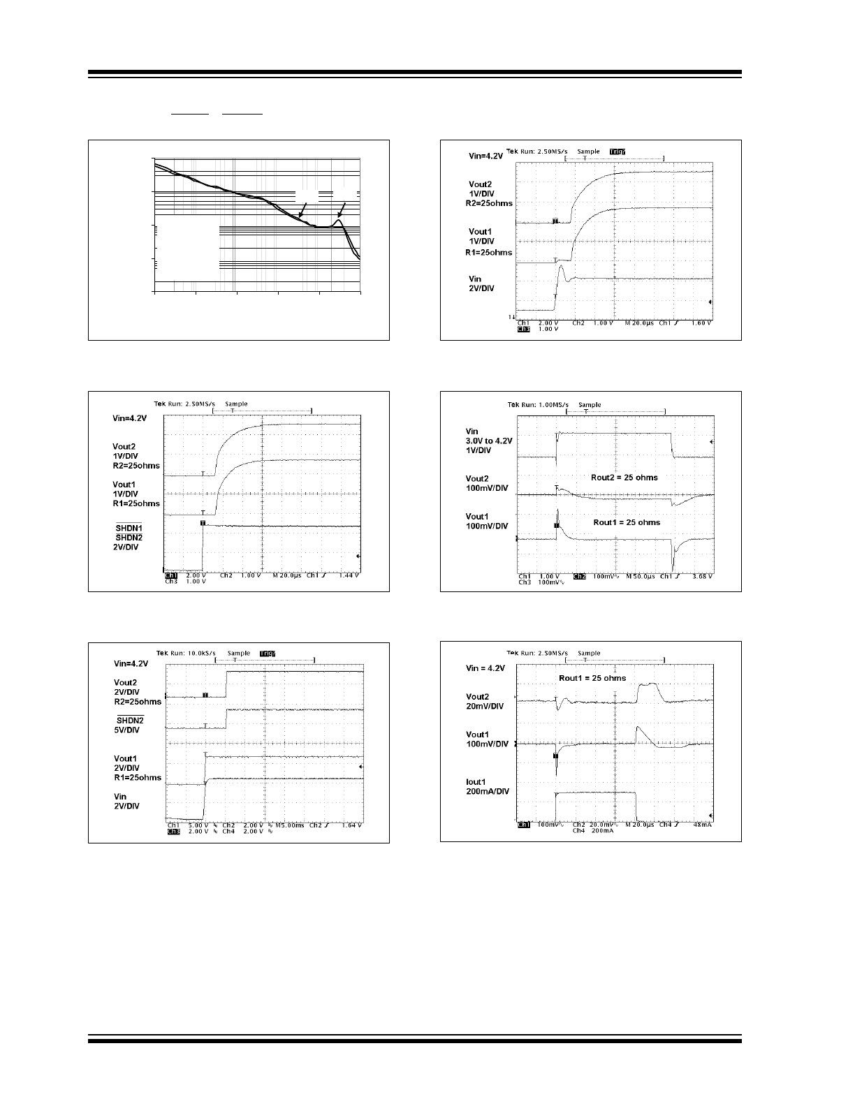
FIGURE 2-19:
V
OUT1
and V
OUT2
Noise vs.
Frequency (with bypass capacitor).
FIGURE 2-20:
V
OUT1
and V
OUT2
Power-up
from Shutdown TC1302B.
FIGURE 2-21:
V
OUT2
Power-up from
Shutdown Input TC1302A.
FIGURE 2-22:
V
OUT1
and V
OUT2
Power-up
from Input Voltage TC1302B.
FIGURE 2-23:
Dynamic Line Response.
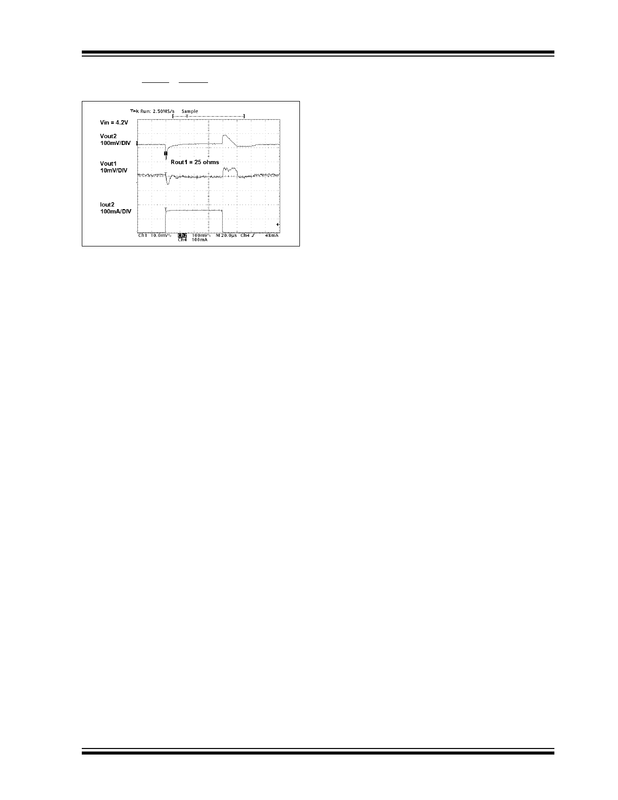
FIGURE 2-24:
300 mA Dynamic Load Step
V
OUT1
.
0.001
0.01
0.1
1
10
0.01
0.1
1
10
100
1000
Frequency (KHz)
NOISE (μV/
Hz)
V
IN
= 4.2V
V
R1
= 2.8V
V
R2
=2.6V
I
OUT1
= 150 mA
I
OUT2
= 100 mA
C
BYPASS
= 10 nF
V
OUT1
V
OUT2
2003-2012 Microchip Technology Inc.
DS21333C-page 9
TC1302A/B
Note: Unless otherwise indicated,
V
IN
= V
R
+1V, I
OUT1
=
I
OUT2
= 100 µA, C
IN
= 4.7 µF, C
OUT1 =
C
OUT2
= 1 µF (X5R or X7R),
C
BYPASS
= 0 pF, SHDN1 = SHDN2 > V
IH
, T
A
= +25°C.
FIGURE 2-25:
150 mA Dynamic Load Step
V
OUT2
.
TC1302A/B
DS21333C-page 10
2003-2012 Microchip Technology Inc.
3.0
TC1302A PIN DESCRIPTIONS
The descriptions of the pins are listed in Table 3-1.
TABLE 3-1:
TC1302A PIN FUNCTION TABLE
3.1
Regulated Output Voltage #1
(V
OUT1
)
Connect V
OUT1
to the positive side of the V
OUT1
capacitor and load. Capable of 300 mA maximum
output current. V
OUT1
output is available when V
IN
is
available; there is no pin to turn it OFF. See TC1302B
if ON/OFF control of V
OUT1
is desired.
3.2
Circuit Ground Pin (GND)
Connect GND to the negative side of the input and
output capacitor. Only the LDO internal circuitry bias
current flows out of this pin (200 µA maximum).
3.3
Reference Bypass Input
By connecting an external 10 nF capacitor (typical) to
the Bypass Input, both outputs (V
OUT1
and V
OUT2
) will
have less noise and improved Power Supply Ripple
Rejection (PSRR) performance. The LDO output
voltage start-up time will increase with the addition of
an external bypass capacitor. By leaving this pin
unconnected, the start-up time will be minimized.
3.4
Output Voltage #2 Shutdown
(SHDN2)
ON/OFF control is performed by connecting SHDN2 to
its proper level. When the input of this pin is connected
to a voltage less than 15% of V
IN
, V
OUT2
will be OFF. If
this pin is connected to a voltage that is greater than
45% of V
IN
, V
OUT2
will be turned ON.
3.5
Regulated Output Voltage #2
(V
OUT2
)
Connect V
OUT2
to the positive side of the V
OUT2
capacitor and load. This pin is capable of a maximum
output current of 150 mA. V
OUT2
can be turned ON and
OFF using SHDN2.
3.6
Unregulated Input Voltage Pin
(V
IN
)
Connect the unregulated input voltage source to V
IN
. If
the input voltage source is located more than several
inches away or is a battery, a typical input capacitance
of 1 µF to 4.7 µF is recommended.
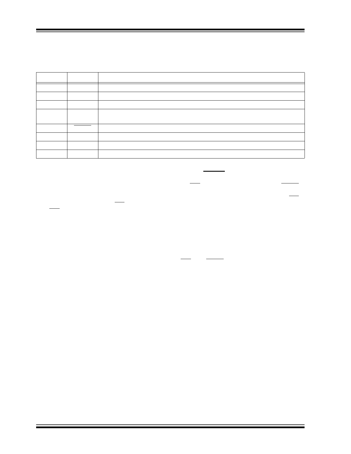
Pin No.
Name
Function
1
NC
No connect.
2
V
OUT1
Regulated output voltage #1, capable of 300 mA.
3
GND
Circuit ground pin.
4
Bypass
Internal reference bypass pin. A 10 nF external capacitor can be used to further reduce
output noise and improve PSRR performance.
5
SHDN2
Output #2 shutdown control input.
6
V
OUT2
Regulated output voltage #2, capable of 150 mA.
7
V
IN
Unregulated input voltage pin.
8
NC
No connect.