
2004 Microchip Technology Inc.
Preliminary
DS21233B-page 1
24C01B/02B
FEATURES
• Single supply with 5.0V operation
• Low power CMOS technology
- 1 mA active current typical
- 10 µA standby current typical at 5.0V
- 5 µA standby current typical at 5.0V
• Organized as a single block of 128 bytes (128 x 8)
or 256 bytes (256 x 8)
• 2-wire serial interface bus, I
2
C compatible
• 100 kHz compatibility
• Self-timed write cycle (including auto-erase)
• Page-write buffer for up to 8 bytes
• 2 ms typical write cycle time for page-write
• Hardware write protect for entire memory
• Can be operated as a serial ROM
• ESD protection > 3,000V
• 1,000,000 ERASE/WRITE cycles guaranteed
Data retention > 200 years
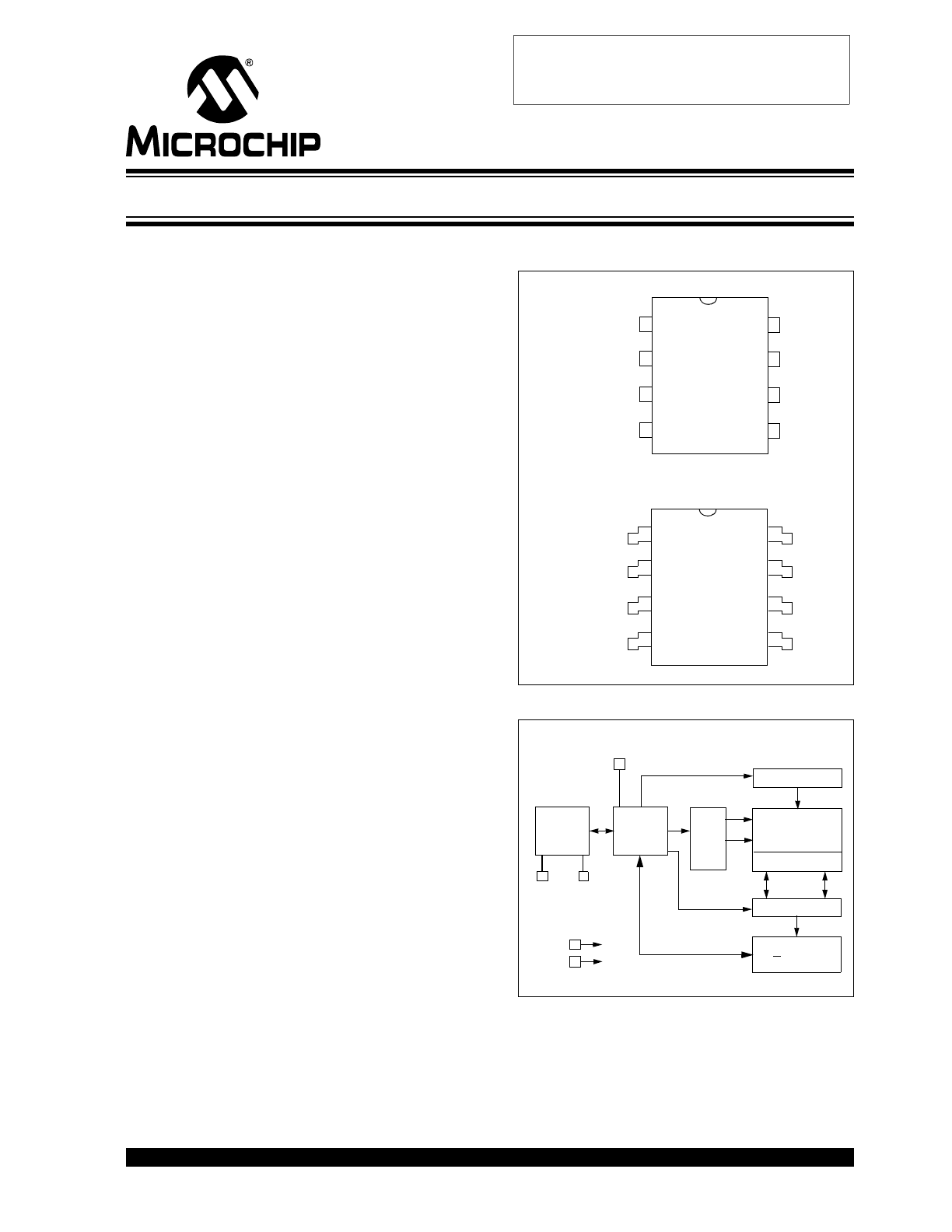
• 8 pin DIP or SOIC package
• Available for extended temperature ranges
DESCRIPTION
The Microchip Technology Inc. 24C01B and 24C02B
are 1K bit and 2K bit Electrically Erasable PROMs. The
devices are organized as a single block of 128 x 8 bit
or 256 x 8 bit memory with a 2-wire serial interface.
The 24C01B and 24C02B also have page-write capa-
bility for up to 8 bytes of data. The 24C01B and 24C02B
are available in the standard 8-pin DIP and an 8-pin
surface mount SOIC package.
These devices are for extended temperature
applications only. It is recommended that all other
applications use Microchip’s 24LC01B/02B.
PACKAGE TYPES
BLOCK DIAGRAM
- Automotive (E):
-40°C to
+125°C
24C
0
1
B
/02
B
24
C
0
1B
/0
2
B
1
2
3
4
8
7
6
5
NC
NC
NC
Vss
Vcc
WP
SCL
SDA
NC
NC
NC
Vss
1
2
3
4
8
7
6
5
Vcc
WP
SCL
SDA
PDIP
SOIC
HV GENERATOR
EEPROM
ARRAY
PAGE LATCHES
YDEC
XDEC
SENSE AMP
R/W CONTROL
MEMORY
CONTROL
LOGIC
I/O
CONTROL
LOGIC
WP
SDA SCL
V
CC
V
SS
1K/2K 5.0V I
2
C
™
Serial EEPROM
I
2
C is a trademark of Philips Corporation.
Obsolete Device
Please use 24LC01B or 24LC02B.
24C01B/02B
DS21233B-page 2
Preliminary
2004 Microchip Technology Inc.
1.0
ELECTRICAL CHARACTERISTICS
1.1
Maximum Ratings*
V
CC
...................................................................................7.0V
All inputs and outputs w.r.t. V
SS
............... -0.6V to V
CC
+1.0V
Storage temperature .....................................-65°C to +150°C
Ambient temp. with power applied ................-65°C to +125°C
Soldering temperature of leads (10 seconds) ............. +300°C
ESD protection on all pins............................................ Š 4 kV
*Notice: Stresses above those listed under “Maximum ratings”
may cause permanent damage to the device. This is a stress rat-
ing only and functional operation of the device at those or any
other conditions above those indicated in the operational listings
of this specification is not implied. Exposure to maximum rating
conditions for extended periods may affect device reliability.
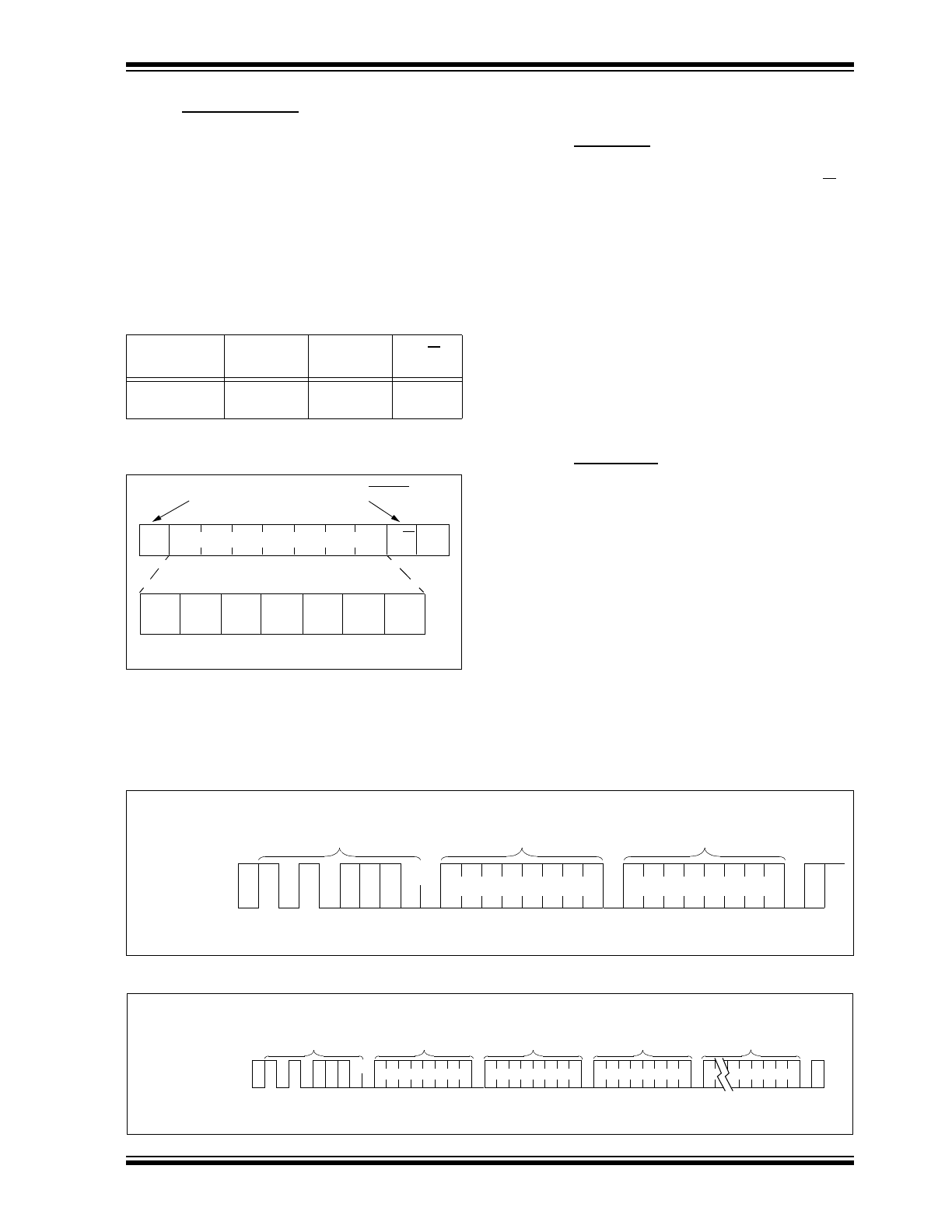
TABLE 1-1:
PIN FUNCTION TABLE
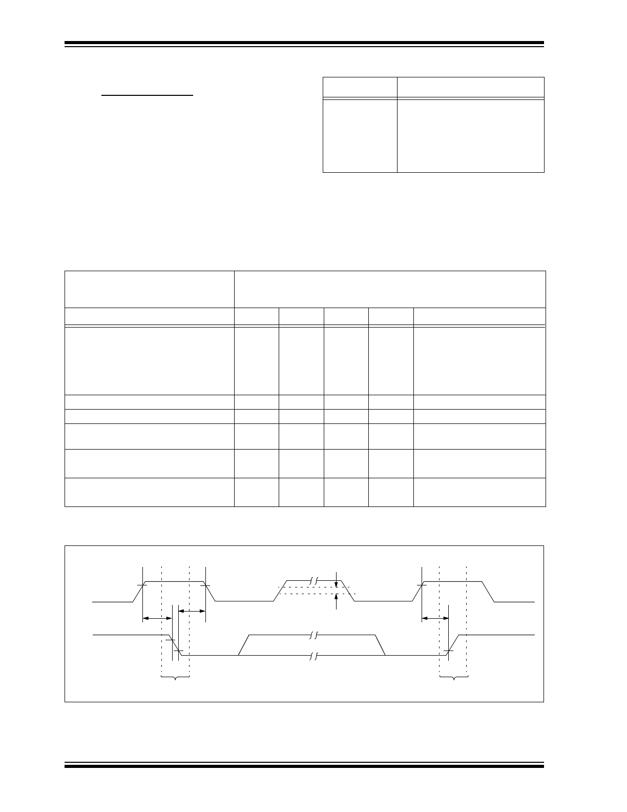
FIGURE 1-1:
BUS TIMING START/STOP
Name
Function
V
SS
SDA
SCL
WP
V
CC
NC
Ground
Serial Address/Data I/O
Serial Clock
Write Protect Input
+5.0V Power Supply
No Internal Connection
TABLE 1-1:
DC CHARACTERISTICS
All parameters apply across the speci-
fied operating ranges unless otherwise
noted.
V
CC
= +4.5V to 5.5V
Automotive (E):
Tamb = -40°C to 125°C
Parameter
Symbol
Min.
Max.
Units
Conditions
WP, SCL and SDA pins:
High level input voltage
V
IH
.7 V
CC
V
Low level input voltage
V
IL
.3 V
CC
V
Hysteresis of Schmidt trigger inputs
V
HYS
.05 V
CC
—
V
(Note)
Low level output voltage
V
OL
.40
V
I
OL
= 3.0 mA, V
CC
= 2.5V
Input leakage current
I
LI
-10
10
µA
V
IN
= .1V to 5.5V
Output leakage current
I
LO
-10
10
µmA
V
OUT
= .1V to 5.5V
Pin capacitance (all inputs/outputs)
C
IN
,
C
OUT
—
10
pF
V
CC
= 5.0V (Note)
Tamb = 25°C, F
CLK
= 1 MHz
Operating current
I
CC
Write
—
3
mA
V
CC
= 5.5V, SCL = 100 kHz
I
CC
Read
—
1
mA
Standby current
I
CCS
—
30
µA
V
CC
= 3.0V, SDA = SCL = V
CC
100
µA
V
CC
= 5.5V, SDA = SCL = V
CC
Note:
This parameter is periodically sampled and not 100% tested.
SCL
SDA
T
SU
:
STA
T
HD
:
STA
START
STOP
V
HYS
T
SU
:
STO
24C01B/02B
2004 Microchip Technology Inc.
Preliminary
DS21233B-page 3
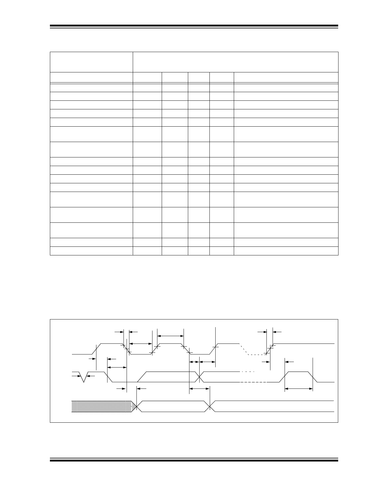
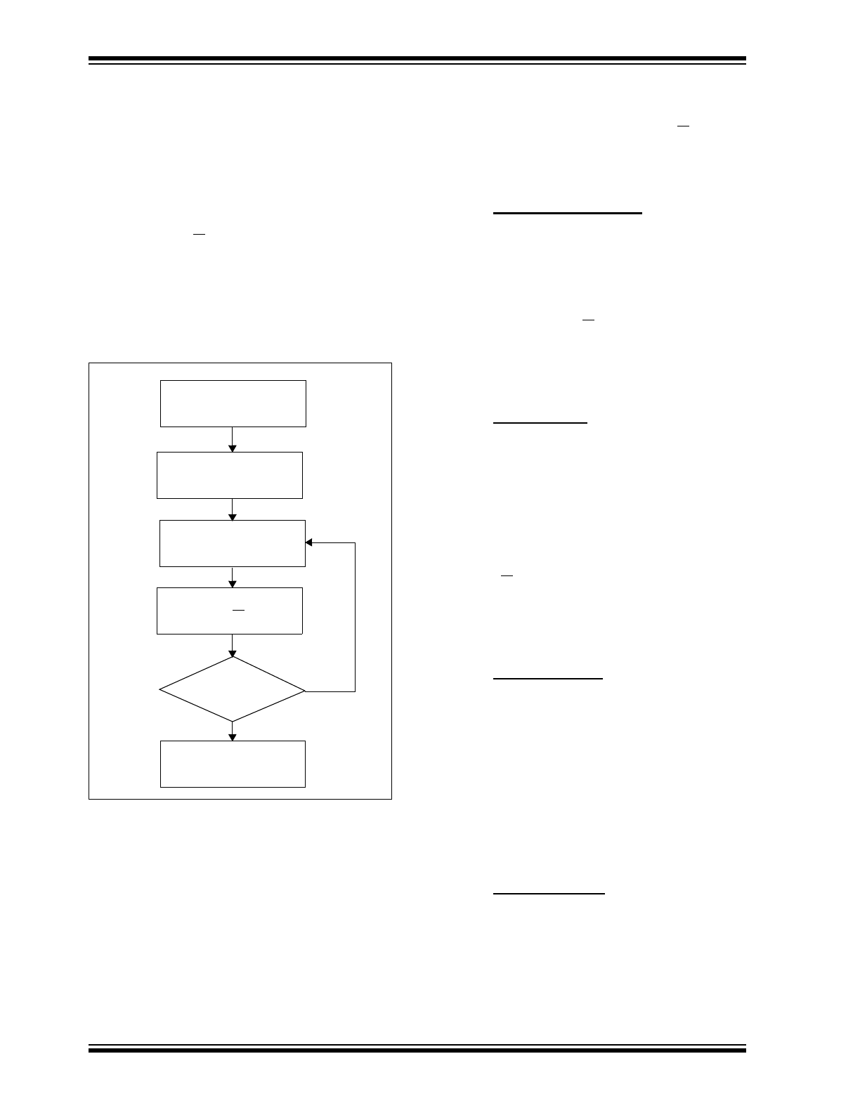
FIGURE 1-2:
BUS TIMING DATA
TABLE 1-2:
AC CHARACTERISTICS
All Parameters apply across the
specified operating ranges unless
otherwise noted
Vcc = 4.5V to 5.5V
Automotive (E):
Tamb = -40°C to +125°C,
Parameter
Symbol
Min.
Max.
Units
Remarks
Clock frequency
F
CLK
—
100
kHz
Clock high time
T
HIGH
4000
—
ns
Clock low time
T
LOW
4700
—
ns
SDA and SCL rise time
T
R
—
1000
ns
(Note 1)
SDA and SCL fall time
T
F
—
300
ns
(Note 1)
START condition hold time
T
HD
:
STA
4000
—
ns
After this period the first clock pulse is
generated
START condition setup time
T
SU
:
STA
4700
—
ns
Only relevant for repeated
START condition
Data input hold time
T
HD
:
DAT
0
—
ns
(Note 2)
Data input setup time
T
SU
:
DAT
250
—
ns
STOP condition setup time
T
SU
:
STO
4000
—
ns
Output valid from clock
T
AA
—
3500
ns
(Note 2)
Bus free time
T
BUF
4700
—
ns
Time the bus must be free before a new
transmission can start
Output fall time from V
IH
minimum to V
IL
maximum
T
OF
—
250
ns
(Note 1), CB ð 100 pF
Input filter spike suppression
(SDA and SCL pins)
T
SP
—
50
ns
(Note 3)
Write cycle time
T
WR
—
10
ms
Byte or Page mode
Endurance
—
1M
—
cycles
25°C, Vcc = 5.0V, Block Mode (Note 4)
Note 1: Not 100% tested. CB = total capacitance of one bus line in pF.
2: As a transmitter, the device must provide an internal minimum delay time to bridge the undefined region
(minimum 300 ns) of the falling edge of SCL to avoid unintended generation of START or STOP conditions.
3: The combined T
SP
and V
HYS
specifications are due to Schmitt trigger inputs which provide improved noise
spike suppression. This eliminates the need for a TI specification for standard operation.
4: This parameter is not tested but guaranteed by characterization. For endurance estimates in a specific
application, please consult the Total Endurance Model which can be obtained on our BBS or website.
SCL
SDA
IN
SDA
OUT
T
HD
:
STA
T
SU
:
STA
T
F
T
HIGH
T
R
T
SU
:
STO
T
SU
:
DAT
T
HD
:
DAT
T
BUF
T
AA
T
HD
:
STA
T
AA
T
SP
T
LOW
24C01B/02B
DS21233B-page 4
Preliminary
2004 Microchip Technology Inc.
2.0
FUNCTIONAL DESCRIPTION
The 24C01B/02B supports a bi-directional two wire bus
and data transmission protocol. A device that sends
data onto the bus is defined as transmitter, and a
device receiving data as receiver. The bus has to be
controlled by a master device which generates the
serial clock (SCL), controls the bus access, and gener-
ates the START and STOP conditions, while the
24C01B/02B works as slave. Both master and slave
can operate as transmitter or receiver but the master
device determines which mode is activated.
3.0
BUS CHARACTERISTICS
The following bus protocol has been defined:
• Data transfer may be initiated only when the bus
is not busy.
• During data transfer, the data line must remain
stable whenever the clock line is HIGH. Changes
in the data line while the clock line is HIGH will be
interpreted as a START or STOP condition.
Accordingly, the following bus conditions have been
defined (Figure 3-1).
3.1
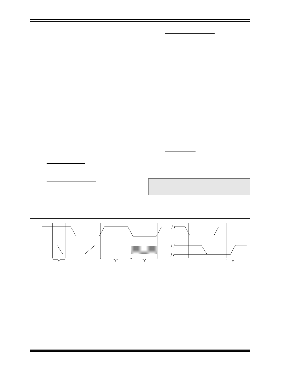
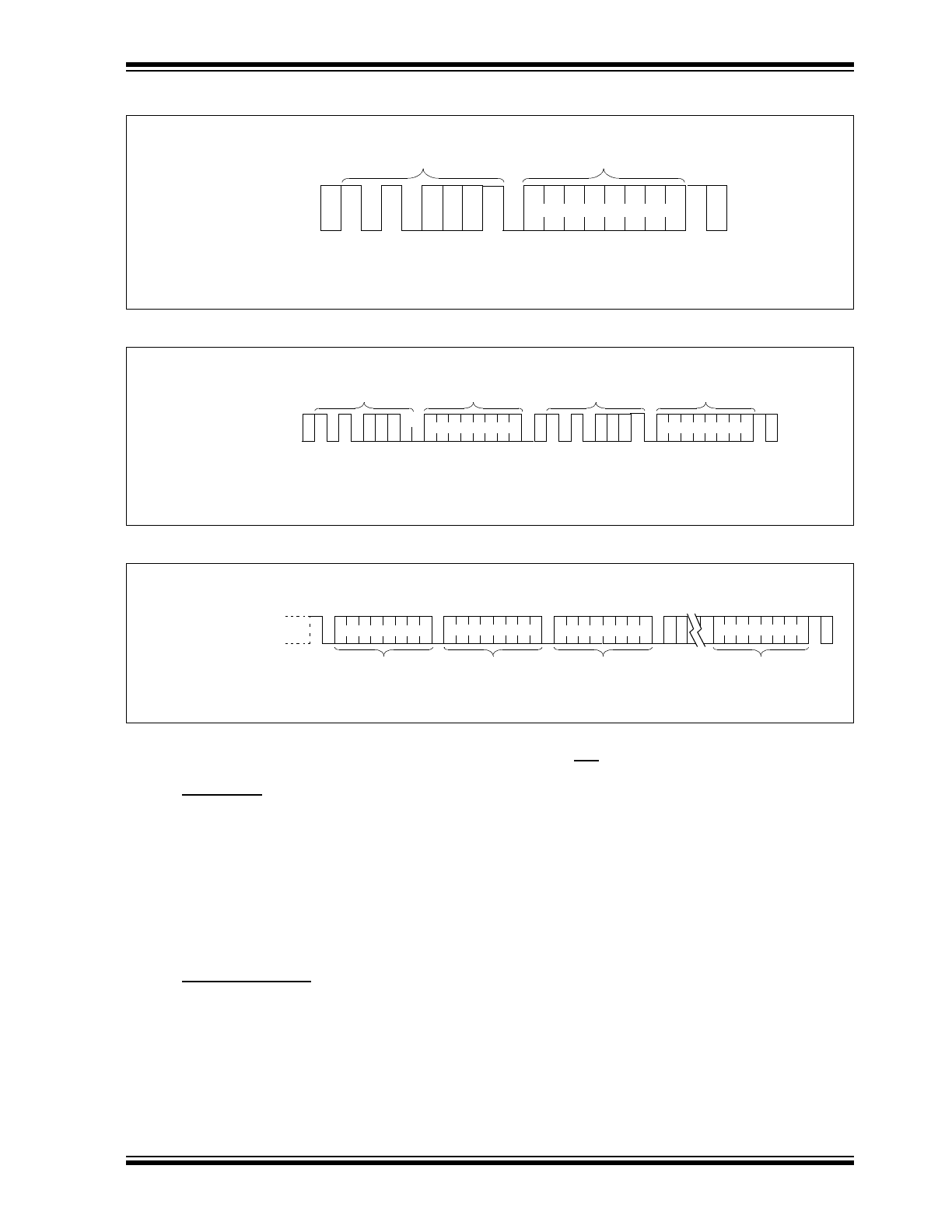
Bus Not Busy (A)
Both data and clock lines remain HIGH.
3.2
Start Data Transfer (B)
A HIGH to LOW transition of the SDA line while the
clock (SCL) is HIGH determines a START condition.
All commands must be preceded by a START condi-
tion.
3.3
Stop Data Transfer (C)
A LOW to HIGH transition of the SDA line while the
clock (SCL) is HIGH determines a STOP condition. All
operations must be ended with a STOP condition.
3.4
Data Valid (D)
The state of the data line represents valid data when,
after a START condition, the data line is stable for the
duration of the HIGH period of the clock signal.
The data on the line must be changed during the LOW
period of the clock signal. There is one clock pulse per
bit of data.
Each data transfer is initiated with a START condition
and terminated with a STOP condition. The number of
the data bytes transferred between the START and
STOP conditions is determined by the master device
and is theoretically unlimited, although only the last six-
teen will be stored when doing a write operation. When
an overwrite does occur it will replace data in a first in
first out fashion.
3.5
Acknowledge
Each receiving device, when addressed, is obliged to
generate an acknowledge after the reception of each
byte. The master device must generate an extra clock
pulse which is associated with this acknowledge bit.
The device that acknowledges has to pull down the
SDA line during the acknowledge clock pulse in such a
FIGURE 3-1:
DATA TRANSFER SEQUENCE ON THE SERIAL BUS
Note:
The 24C01B/02B does not generate any
acknowledge bits if an internal program-
ming cycle is in progress.
SCL
SDA
(
A
)
(B)
(D)
(D)
(C)
(
A
)
START
CONDITION
ADDRESS OR
ACKNOWLEDGE
VALID
DATA
ALLOWED
TO CHANGE
STOP
CONDITION
24C01B/02B
2004 Microchip Technology Inc.
Preliminary
DS21233B-page 5
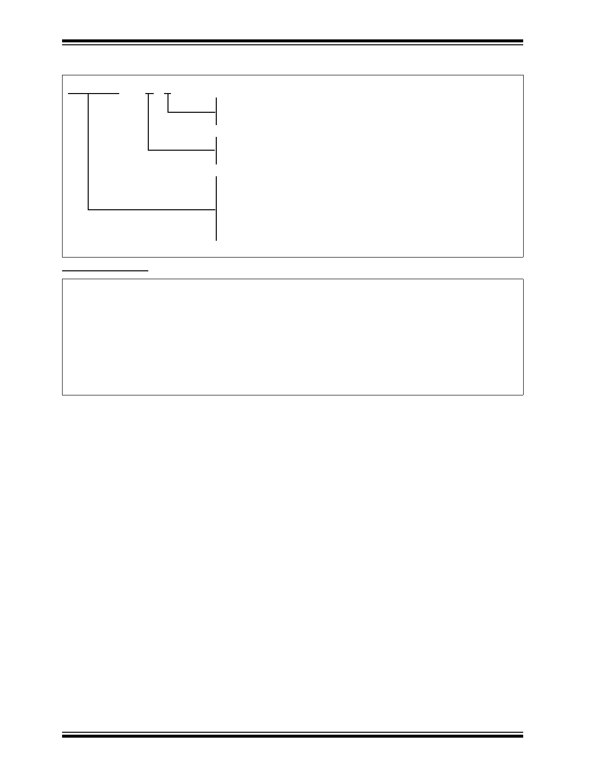
3.6
Device Address
After generating a START condition, the bus master
transmits the slave address consisting of a 4-bit device
code (1010) for the 24C01B/02B, followed by three
don't care bits.
The eighth bit of slave address determines if the master
device wants to read or write to the 24C01B/02B
(Figure 3-2).
The 24C01B/02B monitors the bus for its correspond-
ing slave address all the time. It generates an acknowl-
edge bit if the slave address was true and it is not in a
programming mode.
FIGURE 3-2:
CONTROL BYTE
ALLOCATION
4.0
WRITE OPERATION
4.1
Byte Write
Following the start signal from the master, the device
code (4 bits), the don't care bits (3 bits), and the R/W bit
which is a logic low is placed onto the bus by the master
transmitter. This indicates to the addressed slave
receiver that a byte with a word address will follow after
it has generated an acknowledge bit during the ninth
clock cycle. Therefore the next byte transmitted by the
master is the word address and will be written into the
address pointer of the 24C01B/02B. After receiving
another acknowledge signal from the 24C01B/02B the
master device will transmit the data word to be written
into the addressed memory location. The 24C01B/02B
acknowledges again and the master generates a stop
condition. This initiates the internal write cycle, and
during this time the 24C01B/02B will not generate
acknowledge signals (Figure 4-1).
4.2
Page Write
The write control byte, word address and the first data
byte are transmitted to the 24C01B/02B in the same
way as in a byte write. But instead of generating a stop
condition the master transmits up to eight data bytes to
the 24C01B/02B which are temporarily stored in the
on-chip page buffer and will be written into the memory
after the master has transmitted a stop condition. After
the receipt of each word, the three lower order address
pointer bits are internally incremented by one. The
higher order five bits of the word address remains con-
stant. If the master should transmit more than eight
words prior to generating the stop condition, the
address counter will roll over and the previously
received data will be overwritten. As with the byte write
operation, once the stop condition is received an inter-
nal write cycle will begin (Figure 4-2).
FIGURE 4-1:
BYTE WRITE
FIGURE 4-2:
PAGE WRITE
Operation
Control
Code
Chip
Select
R/W
Read
Write
1010
1010
XXX
XXX
1
0
X = Don’t care
R/W
A
1
0
1
0
X
X
X
READ/WRITE
START
SLAVE ADDRESS
S
P
S
T
A
R
T
S
T
O
P
BUS ACTIVITY
MASTER
SDA LINE
BUS ACTIVITY
A
C
K
A
C
K
A
C
K
CONTROL
BYTE
WORD
ADDRESS
DATA
S
P
BUS ACTIVITY
MASTER
SDA LINE
BUS ACTIVITY
S
T
A
R
T
S
T
O
P
CONTROL
BYTE
WORD
ADDRESS (n)
DATA n
DATAn + 7
DATAn + 1
A
C
K
A
C
K
A
C
K
A
C
K
A
C
K
24C01B/02B
DS21233B-page 6
Preliminary
2004 Microchip Technology Inc.
5.0
ACKNOWLEDGE POLLING
Since the device will not acknowledge during a write
cycle, this can be used to determine when the cycle is
complete (this feature can be used to maximize bus
throughput). Once the stop condition for a write com-
mand has been issued from the master, the device ini-
tiates the internally timed write cycle. ACK polling can
be initiated immediately. This involves the master send-
ing a start condition followed by the control byte for a
write command (R/W = 0). If the device is still busy with
the write cycle, then no ACK will be returned. If the
cycle is complete, then the device will return the ACK
and the master can then proceed with the next read or
write command. See Figure 5-1 for flow diagram.
FIGURE 5-1:
ACKNOWLEDGE POLLING
FLOW
6.0
WRITE PROTECTION
The 24C01B/02B can be used as a serial ROM when
the WP pin is connected to V
CC
. Programming will be
inhibited and the entire memory will be write-protected.
7.0
READ OPERATION
Read operations are initiated in the same way as write
operations with the exception that the R/W bit of the
slave address is set to one. There are three basic types
of read operations: current address read, random read,
and sequential read.
7.1
Current Address Read
The 24C01B/02B contains an address counter that
maintains the address of the last word accessed, inter-
nally incremented by one. Therefore, if the previous
access (either a read or write operation) was to
address n, the next current address read operation
would access data from address n + 1. Upon receipt of
the slave address with R/W bit set to one, the 24C01B/
02B issues an acknowledge and transmits the eight bit
data word. The master will not acknowledge the trans-
fer but does generate a stop condition and the 24C01B/
02B discontinues transmission (Figure 7-1).
7.2
Random Read
Random read operations allow the master to access
any memory location in a random manner. To perform
this type of read operation, first the word address must
be set. This is done by sending the word address to the
24C01B/02B as part of a write operation. After the word
address is sent, the master generates a start condition
following the acknowledge. This terminates the write
operation, but not before the internal address pointer is
set. Then the master issues the control byte again but
with the R/W bit set to a one. The 24C01B/02B will then
issue an acknowledge and transmits the eight bit data
word. The master will not acknowledge the transfer but
does generate a stop condition and the 24C01B/02B
discontinues transmission (Figure 7-2).
7.3
Sequential Read
Sequential reads are initiated in the same way as a ran-
dom read except that after the 24C01B/02B transmits
the first data byte, the master issues an acknowledge
as opposed to a stop condition in a random read. This
directs the 24C01B/02B to transmit the next sequen-
tially addressed 8-bit word (Figure 7-3).
To provide sequential reads the 24C01B/02B contains
an internal address pointer which is incremented by
one at the completion of each operation. This address
pointer allows the entire memory contents to be serially
read during one operation.
7.4
Noise Protection
The 24C01B/02B employs a V
CC
threshold detector
circuit which disables the internal erase/write logic if the
V
CC
is below 1.5 volts at nominal conditions.
The SCL and SDA inputs have Schmitt trigger and filter
circuits which suppress noise spikes to assure proper
device operation even on a noisy bus.
Send
Write Command
Send Stop
Condition to
Initiate Write Cycle
Send Start
Send Control Byte
with R/W = 0
Did Device
Acknowledge
(ACK = 0)?
Next
Operation
NO
YES
24C01B/02B
2004 Microchip Technology Inc.
Preliminary
DS21233B-page 7
FIGURE 7-1:
CURRENT ADDRESS READ
FIGURE 7-2:
RANDOM READ
FIGURE 7-3:
SEQUENTIAL READ
8.0
PIN DESCRIPTIONS
8.1
Serial Data
This is a bi-directional pin used to transfer addresses
and data into and data out of the device. It is an open
drain terminal, therefore the SDA bus requires a pull-up
resistor to V
CC
(typically 10 K¾ for 100 kHz).
For normal data transfer SDA is allowed to change only
during SCL low. Changes during SCL high are
reserved for indicating the START and STOP condi-
tions.
8.2
SCL Serial Clock
This input is used to synchronize the data transfer from
and to the device.
8.3
WP
This pin must be connected to either V
SS
or V
CC
.
If tied to V
SS
, normal memory operation is enabled
(read/write the entire memory).
If tied to V
CC
, WRITE operations are inhibited. The
entire memory will be write-protected. Read operations
are not affected.
This feature allows the user to use the 24C01B/02B as
a serial ROM when WP is enabled (tied to V
CC
).
S
P
BUS ACTIVITY
MASTER
SDA LINE
BUS ACTIVITY
S
T
A
R
T
CONTROL
BYTE
DATA n
A
C
K
N
O
A
C
K
S
T
O
P
S
P
S
BUS ACTIVITY
MASTER
SDA LINE
BUS ACTIVITY
S
T
A
R
T
S
T
O
P
CONTROL
BYTE
WORD
ADDRESS (n)
DATA n
A
C
K
A
C
K
N
O
A
C
K
CONTROL
BYTE
A
C
K
S
T
A
R
T
P
SDA LINE
BUS ACTIVITY
S
T
O
P
CONTROL
BYTE
DATA n
A
C
K
N
O
A
C
K
A
C
K
A
C
K
A
C
K
DATA n + 1
DATA n + 2
DATA n + X
BUS ACTIVITY
MASTER
24C01B/02B
DS21233B-page 8
Preliminary
2004 Microchip Technology Inc.
To order or obtain information, e.g., on pricing or delivery, refer to the factory or the listed sales office.
Sales and Support
24C01B/02B
—
/P
Package:
P = Plastic DIP (300 mil Body), 8-lead
SN = Plastic SOIC (150 mil Body)
Temperature
E = -40°C to +125°C
Range:
Device:
24C01B
1K I
2
C Serial EEPROM
24C01BT
1K I
2
C Serial EEPROM (Tape and Reel)
24C02B
2K I
2
C Serial EEPROM
24C02BT
2K I
2
C Serial EEPROM (Tape and Reel)
Data Sheets
Products supported by a preliminary Data Sheet may have an errata sheet describing minor operational differences and recom-
mended workarounds. To determine if an errata sheet exists for a particular device, please contact one of the following:
1.
Your local Microchip sales office
2.
The Microchip Corporate Literature Center U.S. FAX: (480) 792-7277
3.
The Microchip Worldwide Site (www.microchip.com)
Please specify which device, revision of silicon and Data Sheet (include Literature #) you are using.
New Customer Notification System
Register on our web site (www.microchip.com/cn) to receive the most current information on our products.

2004 Microchip Technology Inc.
Preliminary
DS21233B-page 9
Information contained in this publication regarding device
applications and the like is intended through suggestion only
and may be superseded by updates. It is your responsibility to
ensure that your application meets with your specifications.
No representation or warranty is given and no liability is
assumed by Microchip Technology Incorporated with respect
to the accuracy or use of such information, or infringement of
patents or other intellectual property rights arising from such
use or otherwise. Use of Microchip’s products as critical
components in life support systems is not authorized except
with express written approval by Microchip. No licenses are
conveyed, implicitly or otherwise, under any intellectual
property rights.
Trademarks
The Microchip name and logo, the Microchip logo, Accuron,
dsPIC, K
EE
L
OQ
, micro
ID
, MPLAB, PIC, PICmicro, PICSTART,
PRO MATE, PowerSmart, rfPIC, and SmartShunt are
registered trademarks of Microchip Technology Incorporated
in the U.S.A. and other countries.
AmpLab, FilterLab, MXDEV, MXLAB, PICMASTER, SEEVAL,
SmartSensor and The Embedded Control Solutions Company
are registered trademarks of Microchip Technology
Incorporated in the U.S.A.
Analog-for-the-Digital Age, Application Maestro, dsPICDEM,
dsPICDEM.net, dsPICworks, ECAN, ECONOMONITOR,
FanSense, FlexROM, fuzzyLAB, In-Circuit Serial
Programming, ICSP, ICEPIC, Migratable Memory, MPASM,
MPLIB, MPLINK, MPSIM, PICkit, PICDEM, PICDEM.net,
PICLAB, PICtail, PowerCal, PowerInfo, PowerMate,
PowerTool, rfLAB, rfPICDEM, Select Mode, Smart Serial,
SmartTel and Total Endurance are trademarks of Microchip
Technology Incorporated in the U.S.A. and other countries.
SQTP is a service mark of Microchip Technology Incorporated
in the U.S.A.
All other trademarks mentioned herein are property of their
respective companies.
© 2004, Microchip Technology Incorporated, Printed in the
U.S.A., All Rights Reserved.
Printed on recycled paper.
Note the following details of the code protection feature on Microchip devices:
•
Microchip products meet the specification contained in their particular Microchip Data Sheet.
•
Microchip believes that its family of products is one of the most secure families of its kind on the market today, when used in the
intended manner and under normal conditions.
•
There are dishonest and possibly illegal methods used to breach the code protection feature. All of these methods, to our
knowledge, require using the Microchip products in a manner outside the operating specifications contained in Microchip’s Data
Sheets. Most likely, the person doing so is engaged in theft of intellectual property.
•
Microchip is willing to work with the customer who is concerned about the integrity of their code.
•
Neither Microchip nor any other semiconductor manufacturer can guarantee the security of their code. Code protection does not
mean that we are guaranteeing the product as “unbreakable.”
Code protection is constantly evolving. We at Microchip are committed to continuously improving the code protection features of our
products. Attempts to break Microchip’s code protection feature may be a violation of the Digital Millennium Copyright Act. If such acts
allow unauthorized access to your software or other copyrighted work, you may have a right to sue for relief under that Act.
Microchip received ISO/TS-16949:2002 quality system certification for
its worldwide headquarters, design and wafer fabrication facilities in
Chandler and Tempe, Arizona and Mountain View, California in
October 2003. The Company’s quality system processes and
procedures are for its PICmicro
®
8-bit MCUs, K
EE
L
OQ
®
code hopping
devices, Serial EEPROMs, microperipherals, nonvolatile memory and
analog products. In addition, Microchip’s quality system for the design
and manufacture of development systems is ISO 9001:2000 certified.

Preliminary
2004 Microchip Technology Inc.
AMERICAS
Corporate Office
2355 West Chandler Blvd.
Chandler, AZ 85224-6199
Tel: 480-792-7200
Fax: 480-792-7277
Technical Support: 480-792-7627
Web Address: www.microchip.com
Atlanta
3780 Mansell Road, Suite 130
Alpharetta, GA 30022
Tel: 770-640-0034
Fax: 770-640-0307
Boston
2 Lan Drive, Suite 120
Westford, MA 01886
Tel: 978-692-3848
Fax: 978-692-3821
Chicago
333 Pierce Road, Suite 180
Itasca, IL 60143
Tel: 630-285-0071
Fax: 630-285-0075
Dallas
16200 Addison Road, Suite 255
Addison Plaza
Addison, TX 75001
Tel: 972-818-7423
Fax: 972-818-2924
Detroit
Tri-Atria Office Building
32255 Northwestern Highway, Suite 190
Farmington Hills, MI 48334
Tel: 248-538-2250
Fax: 248-538-2260
Kokomo
2767 S. Albright Road
Kokomo, IN 46902
Tel: 765-864-8360
Fax: 765-864-8387
Los Angeles
25950 Acero St., Suite 200
Mission Viejo, CA 92691
Tel: 949-462-9523
Fax: 949-462-9608
San Jose
1300 Terra Bella Avenue
Mountain View, CA 94043
Tel: 650-215-1444
Fax: 650-961-0286
Toronto
6285 Northam Drive, Suite 108
Mississauga, Ontario L4V 1X5, Canada
Tel: 905-673-0699
Fax: 905-673-6509
ASIA/PACIFIC
Australia
Microchip Technology Australia Pty Ltd
Unit 32 41 Rawson Street
Epping 2121, NSW
Sydney, Australia
Tel: 61-2-9868-6733
Fax: 61-2-9868-6755
China - Beijing
Unit 706B
Wan Tai Bei Hai Bldg.
No. 6 Chaoyangmen Bei Str.
Beijing, 100027, China
Tel: 86-10-85282100
Fax: 86-10-85282104
China - Chengdu
Rm. 2401-2402, 24th Floor,
Ming Xing Financial Tower
No. 88 TIDU Street
Chengdu 610016, China
Tel: 86-28-86766200
Fax: 86-28-86766599
China - Fuzhou
Unit 28F, World Trade Plaza
No. 71 Wusi Road
Fuzhou 350001, China
Tel: 86-591-7503506
Fax: 86-591-7503521
China - Hong Kong SAR
Unit 901-6, Tower 2, Metroplaza
223 Hing Fong Road
Kwai Fong, N.T., Hong Kong
Tel: 852-2401-1200
Fax: 852-2401-3431
China - Shanghai
Room 701, Bldg. B
Far East International Plaza
No. 317 Xian Xia Road
Shanghai, 200051
Tel: 86-21-6275-5700
Fax: 86-21-6275-5060
China - Shenzhen
Rm. 1812, 18/F, Building A, United Plaza
No. 5022 Binhe Road, Futian District
Shenzhen 518033, China
Tel: 86-755-82901380
Fax: 86-755-8295-1393
China - Shunde
Room 401, Hongjian Building, No. 2
Fengxiangnan Road, Ronggui Town, Shunde
District, Foshan City, Guangdong 528303, China
Tel: 86-757-28395507 Fax: 86-757-28395571
China - Qingdao
Rm. B505A, Fullhope Plaza,
No. 12 Hong Kong Central Rd.
Qingdao 266071, China
Tel: 86-532-5027355 Fax: 86-532-5027205
India
Divyasree Chambers
1 Floor, Wing A (A3/A4)
No. 11, O’Shaugnessey Road
Bangalore, 560 025, India
Tel: 91-80-22290061 Fax: 91-80-22290062
Japan
Yusen Shin Yokohama Building 10F
3-17-2, Shin Yokohama, Kohoku-ku,
Yokohama, Kanagawa, 222-0033, Japan
Tel: 81-45-471- 6166 Fax: 81-45-471-6122
Korea
168-1, Youngbo Bldg. 3 Floor
Samsung-Dong, Kangnam-Ku
Seoul, Korea 135-882
Tel: 82-2-554-7200 Fax: 82-2-558-5932 or
82-2-558-5934
Singapore
200 Middle Road
#07-02 Prime Centre
Singapore, 188980
Tel: 65-6334-8870 Fax: 65-6334-8850
Taiwan
Kaohsiung Branch
30F - 1 No. 8
Min Chuan 2nd Road
Kaohsiung 806, Taiwan
Tel: 886-7-536-4816
Fax: 886-7-536-4817
Taiwan
Taiwan Branch
11F-3, No. 207
Tung Hua North Road
Taipei, 105, Taiwan
Tel: 886-2-2717-7175 Fax: 886-2-2545-0139
Taiwan
Taiwan Branch
13F-3, No. 295, Sec. 2, Kung Fu Road
Hsinchu City 300, Taiwan
Tel: 886-3-572-9526
Fax: 886-3-572-6459
EUROPE
Austria
Durisolstrasse 2
A-4600 Wels
Austria
Tel: 43-7242-2244-399
Fax: 43-7242-2244-393
Denmark
Regus Business Centre
Lautrup hoj 1-3
Ballerup DK-2750 Denmark
Tel: 45-4420-9895 Fax: 45-4420-9910
France
Parc d’Activite du Moulin de Massy
43 Rue du Saule Trapu
Batiment A - ler Etage
91300 Massy, France
Tel: 33-1-69-53-63-20
Fax: 33-1-69-30-90-79
Germany
Steinheilstrasse 10
D-85737 Ismaning, Germany
Tel: 49-89-627-144-0
Fax: 49-89-627-144-44
Italy
Via Salvatore Quasimodo, 12
20025 Legnano (MI)
Milan, Italy
Tel: 39-0331-742611
Fax: 39-0331-466781
Netherlands
Waegenburghtplein 4
NL-5152 JR, Drunen, Netherlands
Tel: 31-416-690399
Fax: 31-416-690340
United Kingdom
505 Eskdale Road
Winnersh Triangle
Wokingham
Berkshire, England RG41 5TU
Tel: 44-118-921-5869
Fax: 44-118-921-5820
07/12/04
W
ORLDWIDE
S
ALES
AND
S
ERVICE