
1997-2012 Microchip Technology Inc.
DS21230E-page 1
25AA080/25LC080/25C080
Device Selection Table
Features:
• Low-power CMOS technology:
- Write current: 3 mA maximum
- Read current: 500
A typical
- Standby current: 500 nA typical
• 1024 x 8-bit organization
• 16 byte page
• Write cycle time: 5 ms max.
• Self-timed erase and write cycles
• Block write protection:
- Protect none, 1/4, 1/2 or all of array
• Built-in write protection:
- Power-on/off data protection circuitry
- Write enable latch
- Write-protect pin
• Sequential read
• High reliability:
- Endurance: 1 M cycles
- Data retention: > 200 years
- ESD protection: > 4000V
• 8-pin PDIP and SOIC (150 mil)
• Temperature ranges supported:
Description:
The Microchip Technology Inc. 25AA080/25LC080/
25C080 (25XX080
*
) are 8 Kbit Serial Electrically
Erasable PROMs. The memory is accessed via a
simple Serial Peripheral Interface (SPI) compatible
serial bus. The bus signals required are a clock input
(SCK) plus separate data in (SI) and data out (SO)
lines. Access to the device is controlled through a Chip
Select (CS) input.
Communication to the device can be paused via the
hold pin (HOLD). While the device is paused, transi-
tions on its inputs will be ignored, with the exception of
chip select, allowing the host to service higher priority
interrupts.
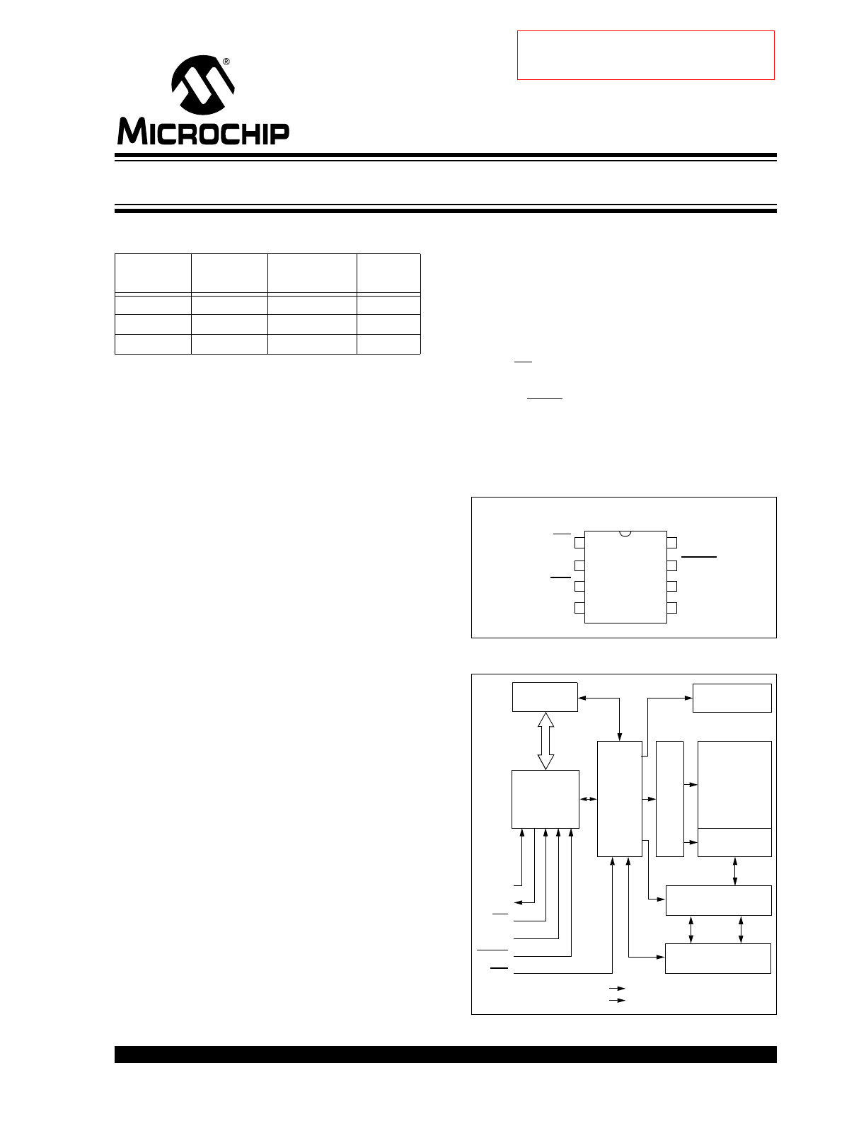
Package Types
Block Diagram
Part
Number
V
CC
Range
Max. Clock
Frequency
Temp.
Ranges
25AA080
1.8-5.5V
1 MHz
I
25LC080
2.5-5.5V
2 MHz
I
25C080
4.5-5.5V
3 MHz
I,E
- Industrial (I):
-40
C to +85C
- Automotive (E) (25C080):
-40°C to +125°C
CS
SO
WP
V
SS
V
CC
HOLD
SCK
SI
1
2
3
4
8
7
6
5
2
5
A
A
080
/
PDIP/SOIC
SI
SO
SCK
CS
HOLD
WP
Status
Register
I/O Control
Memory
Control
Logic
X
Dec
HV Generator
EEPROM
Array
Page Latches
Y Decoder
Sense Amp.
R/W Control
Logic
V
CC
V
SS
8K SPI Bus Serial EEPROM
Not recommended for new designs –
Please use 25AA080A/B or 25LC080A/B.
25AA080/25LC080/25C080
DS21230E-page 2
1997-2012 Microchip Technology Inc.
1.0
ELECTRICAL CHARACTERISTICS
Absolute Maximum Ratings
(†)
V
CC
.............................................................................................................................................................................7.0V
All inputs and outputs w.r.t. V
SS
........................................................................................................ -0.6V to V
CC
+ 1.0V
Storage temperature .................................................................................................................................-65°C to 150°C
Ambient temperature under bias ...............................................................................................................-40°C to 125°C
Soldering temperature of leads (10 seconds) ....................................................................................................... +300°C
ESD protection on all pins ......................................................................................................................................... 4 KV
1.1
DC Characteristics
† NOTICE: Stresses above those listed under ‘Maximum ratings’ may cause permanent damage to the device. This
is a stress rating only and functional operation of the device at those or any other conditions above those indicated in
the operational listings of this specification is not implied. Exposure to maximum rating conditions for an extended
period of time may affect device reliability.
DC CHARACTERISTICS
Industrial (I):
T
A
= -40°C to +85°C
V
CC
= 1.8V to 5.5V
Automotive (E): T
A
= -40°C to +125°C V
CC
= 4.5V to 5.5V (25C080 only)
Param.
No.
Sym.
Characteristic
Min.
Max.
Units
Test Conditions
D001
V
IH
1
High-level input
voltage
2.0
V
CC
+1
V
V
CC
2.7V (Note)
D002
V
IH
2
0.7 V
CC
V
CC
+1
V
V
CC
< 2.7V (Note)
D003
V
IL
1
Low-level input
voltage
-0.3
0.8
V
V
CC
2.7V (Note)
D004
V
IL
2
-0.3
0.3 V
CC
V
V
CC
< 2.7V (Note)
D005
V
OL
Low-level output
voltage
—
0.4
V
I
OL
= 2.1 mA
D006
V
OL
—
0.2
V
I
OL
= 1.0 mA, V
CC
< 2.5V
D007
V
OH
High-level output
voltage
V
CC
-0.5
—
V
I
OH
= -400
A
D008
I
LI
Input leakage current
-10
10
A
CS = V
CC
, V
IN
= V
SS
TO
V
CC
D009
I
LO
Output leakage
current
-10
10
A
CS = V
CC
, V
OUT
= V
SS
TO
V
CC
D010
C
INT
Internal Capacitance
(all inputs and
outputs)
—
7
pF
T
A
= 25°C, CLK = 1.0 MHz,
V
CC
= 5.0V (Note)
D011
I
CC
Read
Operating Current
—
—
1
500
mA
A
V
CC
= 5.5V; F
CLK
= 3.0 MHz;
SO = Open
V
CC
= 2.5V; F
CLK
= 2.0 MHz;
SO = Open
D012
I
CC
Write
—
—
5
3
mA
mA
V
CC
= 5.5V
V
CC
= 2.5V
D013
I
CCS
Standby Current
—
—
5
1
A
A
CS = V
CC
= 5.5V, Inputs tied to V
CC
or
V
SS
CS = V
CC
= 2.5V, Inputs tied to V
CC
or
V
SS
Note:
This parameter is periodically sampled and not 100% tested.
1997-2012 Microchip Technology Inc.
DS21230E-page 3
25AA080/25LC080/25C080
1.2
AC Characteristics
AC CHARACTERISTICS
Industrial (I):
T
A
= -40°C to +85°C
V
CC
= 1.8V to 5.5V
Automotive (E): T
A
= -40°C to +125°C
V
CC
= 4.5V to 5.5V (25C080 only)
Param.
No.
Sym.
Characteristic
Min.
Max.
Units
Test Conditions
1
F
CLK
Clock Frequency
—
—
—
3
2
1
MHz
MHz
MHz
V
CC
= 4.5V to 5.5V
V
CC
= 2.5V to 4.5V
V
CC
= 1.8V to 2.5V
2
T
CSS
CS Setup Time
100
250
500
—
—
—
ns
ns
ns
V
CC
= 4.5V to 5.5V
V
CC
= 2.5V to 4.5V
V
CC
= 1.8V to 2.5V
3
T
CSH
CS Hold Time
150
250
475
—
—
—
ns
ns
ns
V
CC
= 4.5V to 5.5V
V
CC
= 2.5V to 4.5V
V
CC
= 1.8V to 2.5V
4
T
CSD
CS Disable Time
500
—
ns
—
5
Tsu
Data Setup Time
30
50
50
—
—
—
ns
ns
ns
V
CC
= 4.5V to 5.5V
V
CC
= 2.5V to 4.5V
V
CC
= 1.8V to 2.5V
6
T
HD
Data Hold Time
50
100
100
—
—
—
ns
ns
ns
V
CC
= 4.5V to 5.5V
V
CC
= 2.5V to 4.5V
V
CC
= 1.8V to 2.5V
7
T
R
CLK Rise Time
—
2
s
(Note 1)
8
T
F
CLK Fall Time
—
2
s
(Note 1)
9
T
HI
Clock High Time
150
230
475
—
—
—
ns
ns
ns
V
CC
= 4.5V to 5.5V
V
CC
= 2.5V to 4.5V
V
CC
= 1.8V to 2.5V
10
T
LO
Clock Low Time
150
230
475
—
—
—
ns
ns
ns
V
CC
= 4.5V to 5.5V
V
CC
= 2.5V to 4.5V
V
CC
= 1.8V to 2.5V
11
T
CLD
Clock Delay Time
50
—
ns
—
12
T
CLE
Clock Enable Time
50
—
ns
—
13
T
V
Output Valid from Clock Low
—
—
—
150
230
475
ns
ns
ns
V
CC
= 4.5V to 5.5V
V
CC
= 2.5V to 4.5V
V
CC
= 1.8V to 2.5V
14
T
HO
Output Hold Time
0
—
ns
(Note 1)
15
T
DIS
Output Disable Time
—
—
—
200
250
500
ns
ns
ns
V
CC
= 4.5V to 5.5V (Note 1)
V
CC
= 2.5V to 4.5V (Note 1)
V
CC
= 1.8V to 2.5V (Note 1)
16
T
HS
HOLD Setup Time
100
100
200
—
—
—
ns
ns
ns
V
CC
= 4.5V to 5.5V
V
CC
= 2.5V to 4.5V
V
CC
= 1.8V to 2.5V
17
T
HH
HOLD Hold Time
100
100
200
—
—
—
ns
ns
ns
V
CC
= 4.5V to 5.5V
V
CC
= 2.5V to 4.5V
V
CC
= 1.8V to 2.5V
18
T
HZ
HOLD Low to Output High-Z
100
150
200
—
—
—
ns
ns
ns
V
CC
= 4.5V to 5.5V (Note 1)
V
CC
= 2.5V to 4.5V (Note 1)
V
CC
= 1.8V to 2.5V (Note 1)
19
T
HV
HOLD High to Output Valid
100
150
200
—
—
—
ns
ns
ns
V
CC
= 4.5V to 5.5V
V
CC
= 2.5V to 4.5V
V
CC
= 1.8V to 2.5V
20
T
WC
Internal Write Cycle Time
—
5
ms
—
21
—
Endurance
1M
—
E/W
Cycles
(Note 2)
Note 1:
This parameter is periodically sampled and not 100% tested.
2:
This parameter is not tested but ensured by characterization. For endurance estimates in a specific application, please
consult the Total Endurance™ Model which can be obtained from Microchip’s web site at: www.microchip.com.
25AA080/25LC080/25C080
DS21230E-page 4
1997-2012 Microchip Technology Inc.
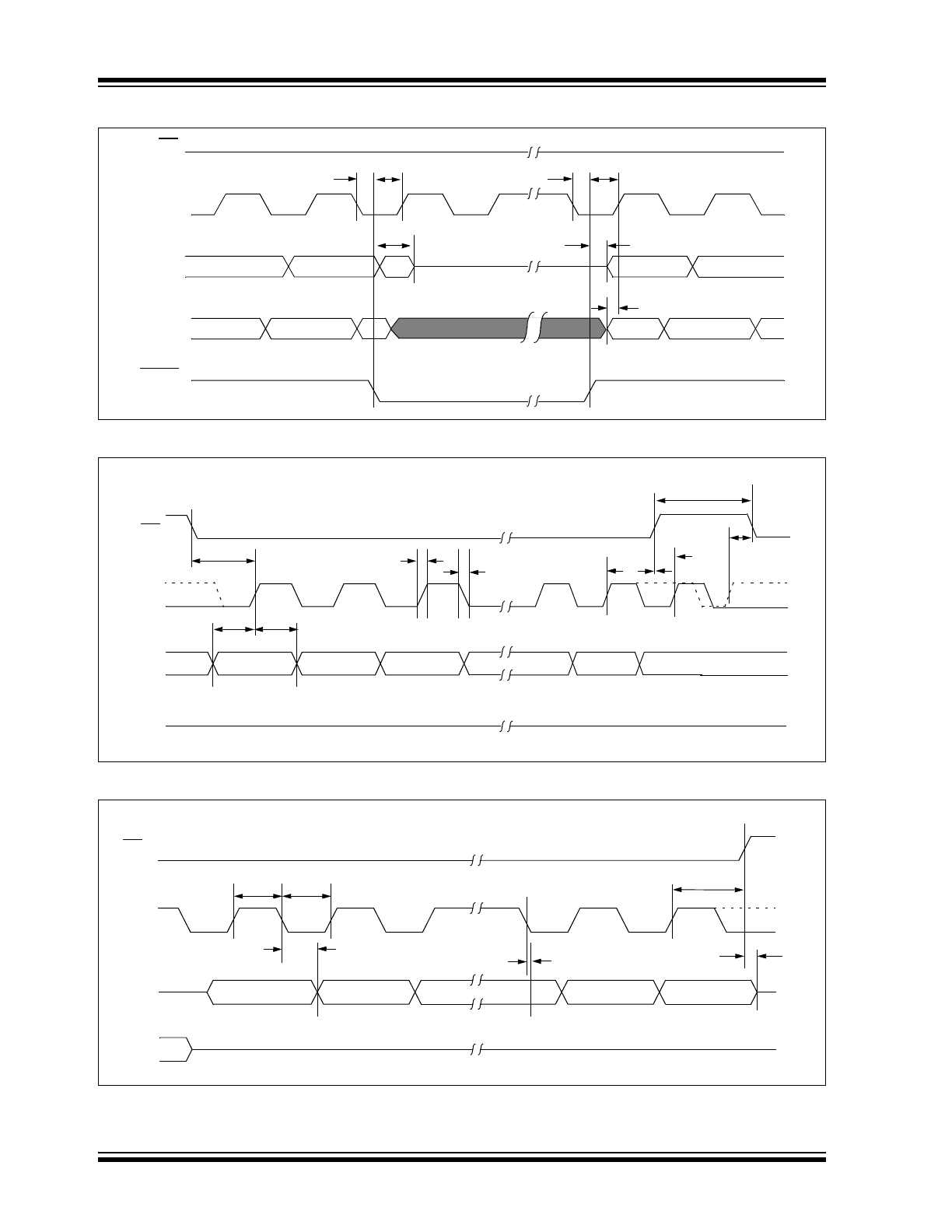
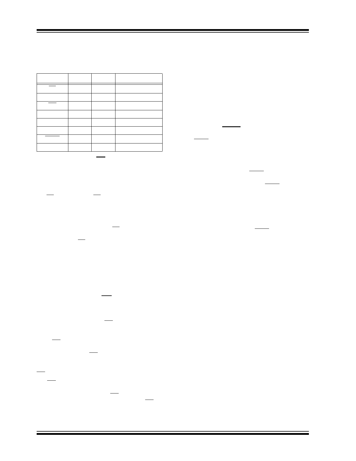
FIGURE 1-1:
HOLD TIMING
FIGURE 1-2:
SERIAL INPUT TIMING
FIGURE 1-3:
SERIAL OUTPUT TIMING
CS
SCK
SO
SI
HOLD
17
16
16
17
19
18
don’t care
5
High-impedance
n+2
n+1
n
n-1
n
n+2
n+1
n
n
n-1
CS
SCK
SI
SO
6
5
8
7
11
3
LSB in
MSB in
High-impedance
12
Mode 1,1
Mode 0,0
2
4
CS
SCK
SO
10
9
13
MSB out
ISB out
3
15
don’t care
SI
Mode 1,1
Mode 0,0
14
1997-2012 Microchip Technology Inc.
DS21230E-page 5
25AA080/25LC080/25C080
1.3
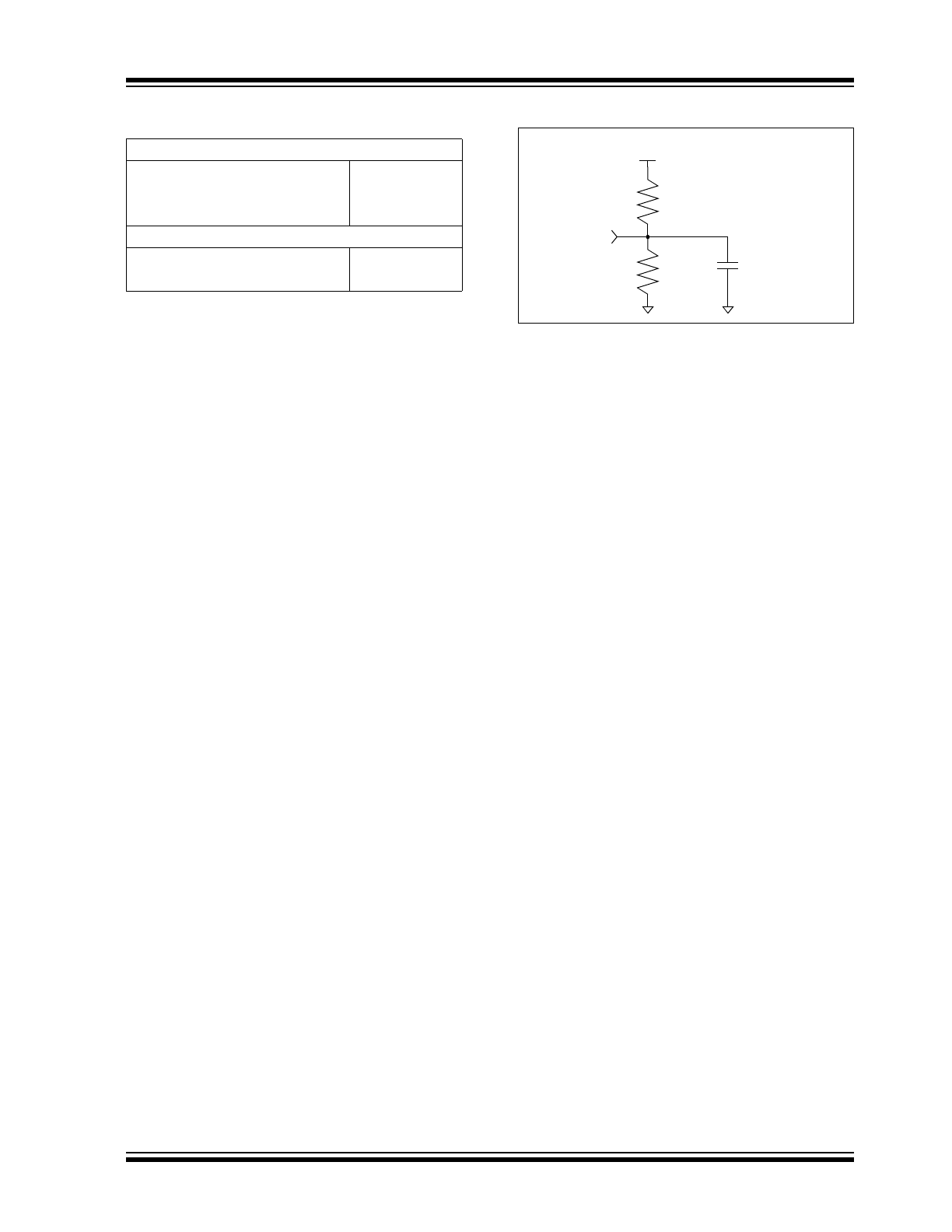
AC Test Conditions
FIGURE 1-4:
AC TEST CIRCUIT
AC Waveform:
V
LO
= 0.2V
—
V
H I
= V
CC
- 0.2V
(Note 1)
V
H I
= 4.0V
(Note 2)
Timing Measurement Reference Level
Input
0.5 V
CC
Output
0.5 V
CC
Note 1: For V
CC
4.0V
2: For V
CC
> 4.0V
V
CC
SO
100 pF
1.8 K
2.25 K
25AA080/25LC080/25C080
DS21230E-page 6
1997-2012 Microchip Technology Inc.
2.0
PIN DESCRIPTIONS
The descriptions of the pins are listed in Table 2-1.
TABLE 2-1:
PIN FUNCTION TABLE
2.1
Chip Select (CS)
A low level on this pin selects the device. A high level
deselects the device and forces it into Standby mode.
However, a programming cycle which is already
initiated or in progress will be completed, regardless of
the CS input signal. If CS is brought high during a
program cycle, the device will go into Standby mode as
soon as the programming cycle is complete. When the
device is deselected, SO goes to the high-impedance
state, allowing multiple parts to share the same SPI
bus. A low-to-high transition on CS after a valid write
sequence initiates an internal write cycle. After power-
up, a low level on CS is required prior to any sequence
being initiated.
2.2
Serial Output (SO)
The SO pin is used to transfer data out of the 25XX080.
During a read cycle, data is shifted out on this pin after
the falling edge of the serial clock.
2.3
Write-Protect (WP)
This pin is used in conjunction with the WPEN bit in the
Status register to prohibit writes to the nonvolatile bits
in the Status register. When WP is low and WPEN is
high, writing to the nonvolatile bits in the Status register
is disabled. All other operations function normally.
When WP is high, all functions, including writes to the
nonvolatile bits in the Status register operate normally.
If the WPEN bit is set, WP low during a Status register
write sequence will disable writing to the Status
register. If an internal write cycle has already begun,
WP going low will have no effect on the write.
The WP pin function is blocked when the WPEN bit in
the Status register is low. This allows the user to install
the 25XX080 in a system with WP pin grounded and
still be able to write to the Status register. The WP pin
functions will be enabled when the WPEN bit is set
high.
2.4
Serial Input (SI)
The SI pin is used to transfer data into the device. It
receives instructions, addresses and data. Data is
latched on the rising edge of the serial clock.
2.5
Serial Clock (SCK)
The SCK is used to synchronize the communication
between a master and the 25XX080. Instructions,
addresses or data present on the SI pin are latched on
the rising edge of the clock input, while data on the SO
pin is updated after the falling edge of the clock input.
2.6
Hold (HOLD)
The HOLD pin is used to suspend transmission to the
25XX080 while in the middle of a serial sequence
without having to retransmit the entire sequence again.
It must be held high any time this function is not being
used. Once the device is selected and a serial
sequence is underway, the HOLD pin may be pulled
low to pause further serial communication without
resetting the serial sequence. The HOLD pin must be
brought low while SCK is low, otherwise the HOLD
function will not be invoked until the next SCK high-to-
low transition. The 25XX080 must remain selected
during this sequence. The SI, SCK and SO pins are in
a high-impedance state during the time the device is
paused and transitions on these pins will be ignored. To
resume serial communication, HOLD must be brought
high while the SCK pin is low, otherwise serial commu-
nication will not resume. Lowering the HOLD line at any
time will tri-state the SO line.
Name
PDIP
SOIC
Function
CS
1
1
Chip Select Input
SO
2
2
Serial Data Output
WP
3
3
Write-Protect Pin
Vss
4
4
Ground
SI
5
5
Serial Data Input
SCK
6
6
Serial Clock Input
HOLD
7
7
Hold Input
Vcc
8
8
Supply Voltage

1997-2012 Microchip Technology Inc.
DS21230E-page 7
25AA080/25LC080/25C080
3.0
FUNCTIONAL DESCRIPTION
3.1
Principles of Operation
The 25XX080 are 1024 byte Serial EEPROMs
designed to interface directly with the Serial Peripheral
Interface (SPI) port of many of today’s popular micro-
controller families, including Microchip’s PIC16C6X/7X
microcontrollers. It may also interface with microcon-
trollers that do not have a built-in SPI port by using
discrete I/O lines programmed properly with the
software.
The 25XX080 contains an 8-bit instruction register. The
device is accessed via the SI pin, with data being
clocked in on the rising edge of SCK. The CS pin must
be low and the HOLD pin must be high for the entire
operation. The WP pin must be held high to allow
writing to the memory array.
Table 3-1 contains a list of the possible instruction
bytes and format for device operation. All instructions,
addresses, and data are transferred MSB first, LSB
last.
Data is sampled on the first rising edge of SCK after CS
goes low. If the clock line is shared with other periph-
eral devices on the SPI bus, the user can assert the
HOLD input and place the 25XX080 in ‘HOLD’ mode.
After releasing the HOLD pin, operation will resume
from the point when the HOLD was asserted.
3.2
Read Sequence
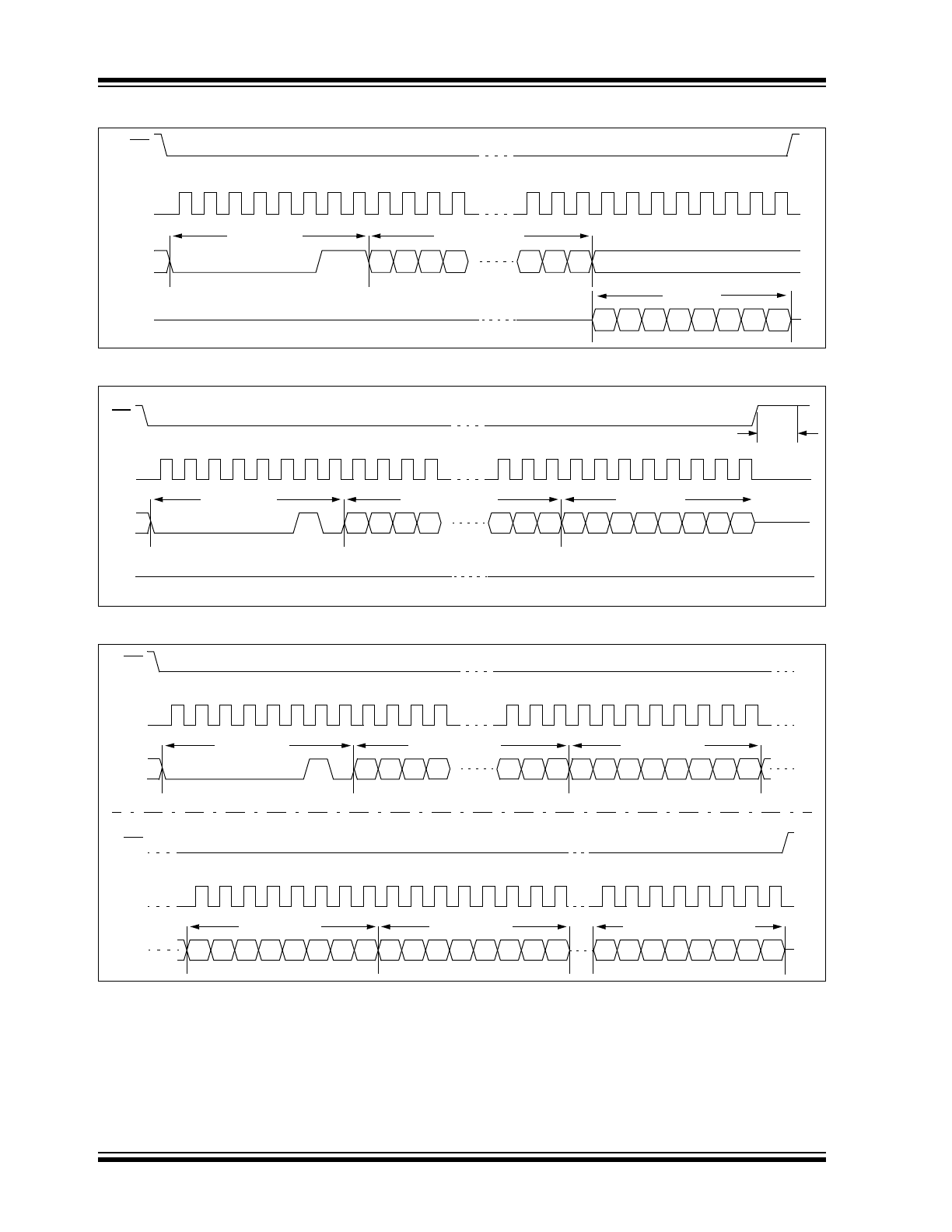
The device is selected by pulling CS low. The 8-bit READ
instruction is transmitted to the 25XX080 followed by
the 16-bit address, with the six MSBs of the address
being "don’t care" bits. After the correct READ instruction
and address are sent, the data stored in the memory at
the selected address is shifted out on the SO pin. The
data stored in the memory at the next address can be
read sequentially by continuing to provide clock pulses.
The internal address pointer is automatically incre-
mented to the next higher address after each byte of
data is shifted out. When the highest address is reached
(03FFh), the address counter rolls over to address
0000h allowing the read cycle to be continued indefi-
nitely. The read operation is terminated by raising the
CS pin (Figure 3-1).
3.3
Write Sequence
Prior to any attempt to write data to the 25XX080, the
write enable latch must be set by issuing the WREN
instruction (Figure 3-4). This is done by setting CS low
and then clocking out the proper instruction into the
25XX080. After all eight bits of the instruction are trans-
mitted, the CS must be brought high to set the write
enable latch. If the write operation is initiated immedi-
ately after the WREN instruction without CS being
brought high, the data will not be written to the array
because the write enable latch will not have been
properly set.
Once the write enable latch is set, the user may
proceed by setting the CS low, issuing a WRITE instruc-
tion, followed by the 16-bit address, with the six MSBs
of the address being “don’t care” bits, and then the data
to be written. Up to 16 bytes of data can be sent to the
25XX080 before a write cycle is necessary. The only
restriction is that all of the bytes must reside in the
same page. A page address begins with
xxxx
xxxx
xxxx
0000
and ends with
xxxx
xxxx
xxxx
1111
.
If the internal address counter reaches
xxxx
xxxx
xxxx
1111
and the clock continues, the counter will
roll back to the first address of the page and overwrite
any data in the page that may have been written.
For the data to be actually written to the array, the CS
must be brought high after the Least Significant bit (D0)
of the n
th
data byte has been clocked in. If CS is
brought high at any other time, the write operation will
not be completed. Refer to Figure 3-2 and Figure 3-3
for more detailed illustrations on the byte write
sequence and the page write sequence respectively.
While the write is in progress, the Status register may
be read to check the status of the WPEN, WIP, WEL,
BP1 and BP0 bits (Figure 3-6). A read attempt of a
memory array location will not be possible during a
write cycle. When the write cycle is completed, the
write enable latch is reset.
TABLE 3-1:
INSTRUCTION SET
Instruction Name
Instruction Format
Description
READ
0000 0011
Read data from memory array beginning at selected address
WRITE
0000 0010
Write data to memory array beginning at selected address
WRDI
0000 0100
Reset the write enable latch (disable write operations)
WREN
0000 0110
Set the write enable latch (enable write operations)
RDSR
0000 0101
Read Status register
WRSR
0000 0001
Write Status register
25AA080/25LC080/25C080
DS21230E-page 8
1997-2012 Microchip Technology Inc.
FIGURE 3-1:
READ SEQUENCE
FIGURE 3-2:
BYTE WRITE SEQUENCE
FIGURE 3-3:
PAGE WRITE SEQUENCE
SO
SI
SCK
CS
0
2
3
4
5
6
7
8
9 10 11
21 22 23 24 25 26 27 28 29 30 31
1
0
1
0
0
0
0
0
1
15 14 13 12
2
1
0
7
6
5
4
3
2
1
0
instruction
16-bit address
data out
High-impedance
SO
SI
CS
9 10 11
21 22 23 24 25 26 27 28 29 30 31
0
0
0
0
0
0
0
1
15 14 13 12
2
1
0
7
6
5
4
3
2
1
0
instruction
16-bit address
data byte
High-impedance
SCK
0
2
3
4
5
6
7
1
8
Twc
SI
CS
9 10 11
21 22 23 24 25 26 27 28 29 30 31
0
0
0
0
0
0
0
1
15 14 13 12
2
1
0
7
6
5
4
3
2
1
0
instruction
16-bit address
data byte 1
SCK
0
2
3
4
5
6
7
1
8
SI
CS
41 42 43
46 47
7
6
5
4
3
2
1
0
data byte n (16 max)
SCK
32
34 35 36 37 38 39
33
40
7
6
5
4
3
2
1
0
data byte 3
7
6
5
4
3
2
1
0
data byte 2
44 45
1997-2012 Microchip Technology Inc.
DS21230E-page 9
25AA080/25LC080/25C080
3.4
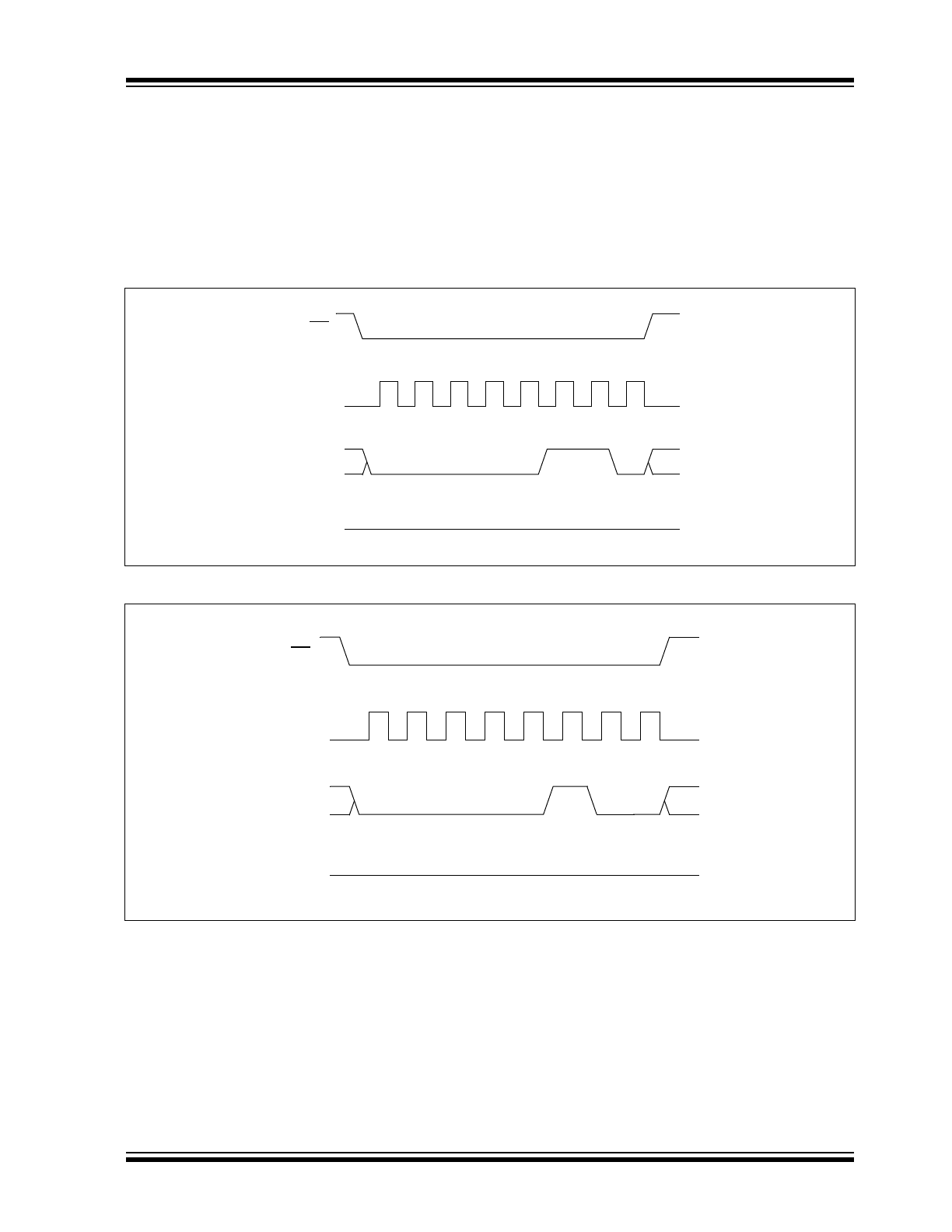
Write Enable (WREN) and Write
Disable (WRDI)
The 25XX080 contains a write enable latch. See
Table 3-3 for the Write-Protect Functionality Matrix.
This latch must be set before any write operation will be
completed internally. The WREN instruction will set the
latch, and the WRDI will reset the latch.
The following is a list of conditions under which the
write enable latch will be reset:
• Power-up
• WRDI instruction successfully executed
• WRSR instruction successfully executed
• WRITE instruction successfully executed
FIGURE 3-4:
WRITE ENABLE SEQUENCE
FIGURE 3-5:
WRITE DISABLE SEQUENCE
SCK
0
2
3
4
5
6
7
1
SI
High-impedance
SO
CS
0
1
0
0
0
0
0
1
SCK
0
2
3
4
5
6
7
1
SI
High-impedance
SO
CS
0
1
0
0
0
0
0
10
25AA080/25LC080/25C080
DS21230E-page 10
1997-2012 Microchip Technology Inc.
3.5
Read Status Register (RDSR)
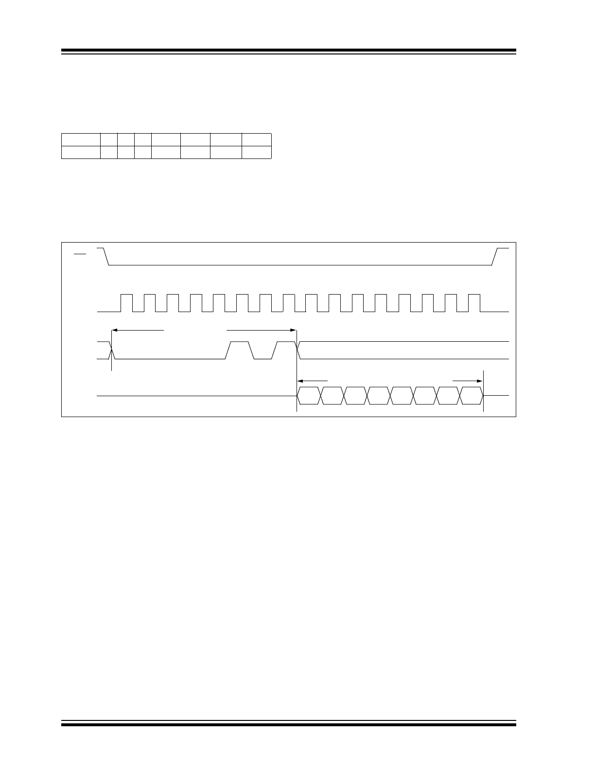
The Read Status Register (RDSR) instruction provides
access to the Status register. The Status register may
be read at any time, even during a write cycle. The
Status register is formatted as follows:
The Write-In-Process (WIP) bit indicates whether the
25XX080 is busy with a write operation. When set to a
‘
1
’, a write is in progress, when set to a ‘
0
’, no write is
in progress. This bit is read-only.
The Write Enable Latch (WEL) bit indicates the status
of the write enable latch. When set to a ‘
1
’, the latch
allows writes to the array, when set to a ‘
0
’, the latch
prohibits writes to the array. The state of this bit can
always be updated via the WREN or WRDI commands
regardless of the state of write protection on the Status
register. This bit is read only.
The Block Protection (BP0 and BP1) bits indicate
which blocks are currently write-protected. These bits
are set by the user issuing the WRSR instruction. These
bits are nonvolatile.
See Figure 3-6 for the RDSR timing sequence.
FIGURE 3-6:
READ STATUS REGISTER TIMING SEQUENCE
7
6
5
4
3
2
1
0
WPEN
X
X
X
BP1
BP0
WEL
WIP
SO
SI
CS
9
10
11
12
13
14
15
1
1
0
0
0
0
0
0
7
6
5
4
2
1
0
instruction
data from Status register
High-impedance
SCK
0
2
3
4
5
6
7
1
8
3