
2004 Microchip Technology Inc.
DS21226E-page 1
24LCS61/24LCS62
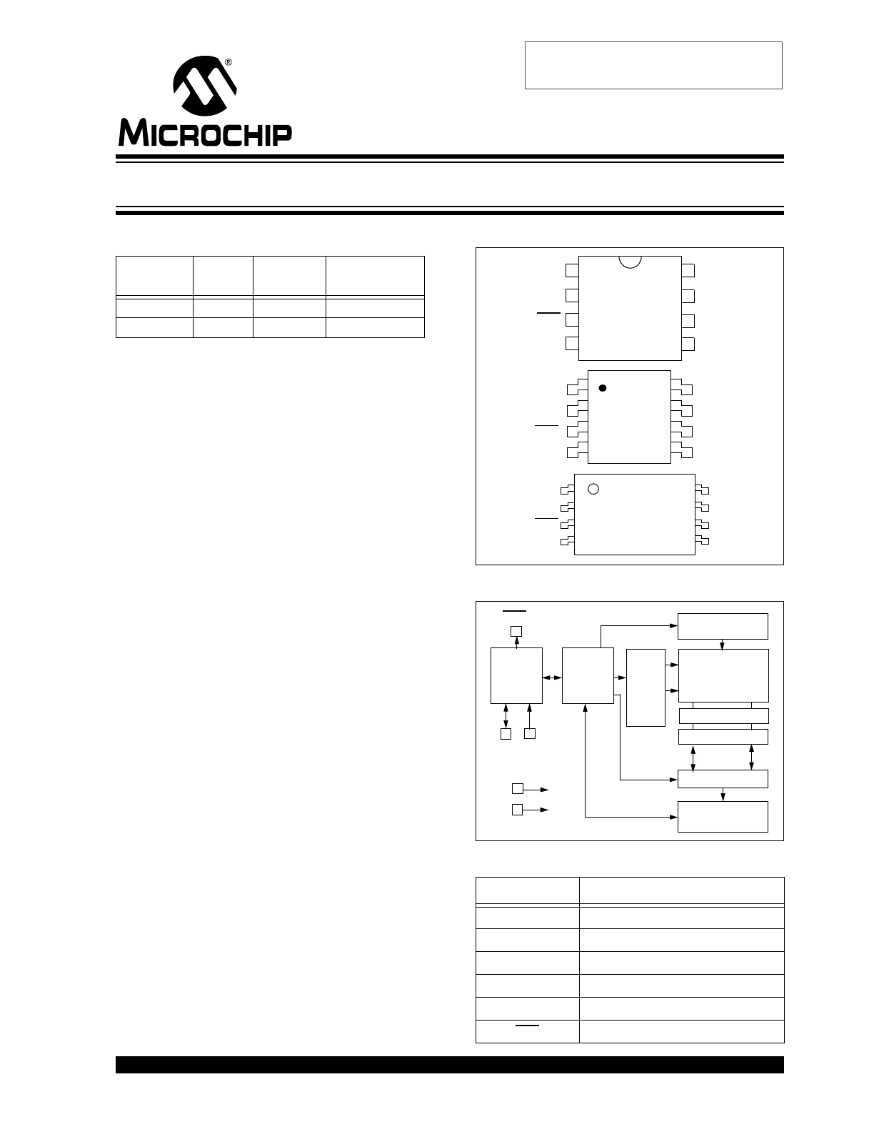
Device Selection Table
Features
• Low-power CMOS technology
- 1 mA active current typical
- 10
µ
A standby current typical at 5.5V
• Software addressability allows up to 255 devices
on the same bus
• 2-wire serial interface bus, I
2
C compatible
• Automatic bus arbitration
• Wakes up to control code 0110
• General purpose output pin can be used to enable
other circuitry
• 100 kHz and 400 kHz compatibility
• Page write buffer for up to 16 bytes
• 10 ms max write cycle time for byte or page write
• 1,000,000 erase/write cycles
• 8-pin PDIP, SOIC or TSSOP packages
• Temperature ranges supported:
Description
The Microchip Technology Inc. 24LCS61/62 is a 1K/2K
bit Serial EEPROM developed for applications that
require many devices on the same bus but do not have
the I/O pins required to address each one individually.
These devices contain an 8 bit address register that is
set upon power-up and allows the connection of up to
255 devices on the same bus. When the process of
assigning ID values to each device is in progress, the
device will automatically handle bus arbitration if more
than one device is operating on the bus. In addition, an
external open drain output pin is available that can be
used to enable other circuitry associated with each
individual system. Low current design permits
operation with typical standby and active currents of
only 10
µ
A and 1 mA respectively. The device has a
page write capability for up to 16 bytes of data. The
device is available in the standard 8-pin PDIP, SOIC
(150 mil), and TSSOP packages.
Package Types
Block Diagram
Pin Function Table
Device
Array
Size
Voltage
Range
Software Write
Protection
24LCS51
1K bits
2.5V-5.5V
Entire Array
24LCS62
2K bits
2.5V-5.5V
Lower Half
- Industrial (I):
-40°C to +85°C
Name
Function
V
SS
Ground
SDA
Serial Data
SCL
Serial Clock
V
CC
+2.5V to 5.5V Power Supply
NC
No Internal Connection
EDS
External Device Select Output
PDIP
NC
NC
EDS
Vss
Vcc
NC
SCL
SDA
24L
CS
61/
62
1
2
3
4
8
7
6
5
NC
NC
EDS
Vss
V
CC
NC
SCL
SDA
24L
CS61/
62
1
2
3
4
8
7
6
5
SOIC
TSSOP
24L
CS61/
62
NC
NC
EDS
V
SS
Vcc
NC
SCL
SDA
1
2
3
4
8
7
6
5
I/O
Control
Logic
Memory
Control
Logic
XDEC
HV Generator
EEPROM
Array
YDEC
V
CC
V
SS
Sense Amp.
R/W Control
SDA SCL
EDS
ID Register
Serial Number
1K/2K Software Addressable I
2
C
™
Serial EEPROM
I
2
C is a trademark of Philips Corporation.
Obsolete Device
24LCS61/24LCS62
DS21226E-page 2
2004 Microchip Technology Inc.
1.0
ELECTRICAL CHARACTERISTICS
Absolute Maximum Ratings
(†)
V
CC
.............................................................................................................................................................................7.0V
All inputs and outputs w.r.t. V
SS
......................................................................................................... -0.6V to V
CC
+1.0V
Storage temperature ...............................................................................................................................-65°C to +150°C
Ambient temperature with power applied ................................................................................................-65°C to +125°C
ESD protection on all pins
......................................................................................................................................................≥
4 kV
† NOTICE: Stresses above those listed under “Absolute Maximum Ratings” may cause permanent damage to
the device. This is a stress rating only and functional operation of the device at those or any other conditions
above those indicated in the operational listings of this specification is not implied. Exposure to maximum rating
conditions for extended periods may affect device reliability.
TABLE 1-1:
DC CHARACTERISTICS
All parameters apply across the
specified operating ranges unless
otherwise noted.
V
CC
= +2.5V to +5.5V
Industrial (I): T
A
= -40°C to +85°C
Parameter
Symbol
Min.
Max.
Units
Conditions
SCL and SDA pins:
High-level input voltage
V
IH
0.7 V
CC
—
V
Low-level input voltage
V
IL
—
.3 V
CC
V
Hysteresis of Schmitt Trigger
inputs
V
HYS
0.05 V
CC
—
V
Low-level output voltage
(SDA and EDS pins)
V
OL
—
.40
V
I
OL
= 12 mA, V
CC
= 4.5V
I
OL
= 8 mA, V
CC
= 2.5V
Input leakage current
I
LI
—
±1
µ
A
V
IN
= Vss or Vcc
Output leakage current
I
LO
—
±1
µ
A
V
OUT
= Vss or Vcc
Pin capacitance (all inputs/outputs)
C
IN
,
C
OUT
—
10
pF
V
CC
= 5.0V (Note)
T
A
= 25°C, f = 1 MHz
Operating current
I
CC
Write
—
4
mA
V
CC
= 5.5V
I
CC
Read
—
1
mA
V
CC
= 5.5V, SCL = 400 kHz
Standby current
I
CCS
—
50
µ
A
V
CC
= 5.5V, SDA = SCL = V
CC
EDS = V
CC
Note:
This parameter is periodically sampled and not 100% tested.
2004 Microchip Technology Inc.
DS21226E-page 3
24LCS61/24LCS62
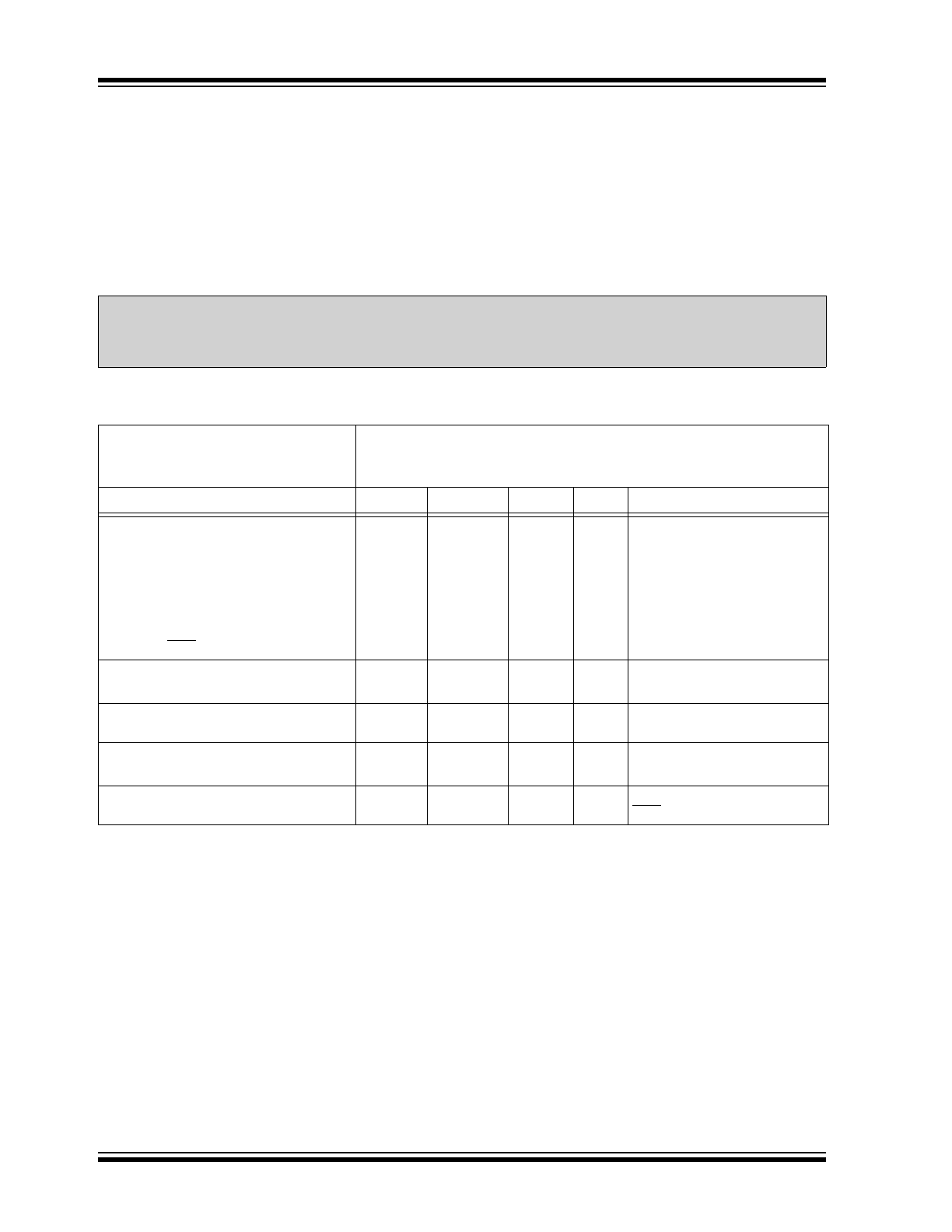
TABLE 1-2:
AC CHARACTERISTICS
FIGURE 1-1:
BUS TIMING DATA
All parameters apply across the specified
operating ranges unless otherwise noted.
Vcc = +2.5V to 5.5V
Industrial (I): T
A
= -40°C to +85°C
Parameter
Symbol
V
CC
= 2.5V - 5.5V
STD MODE
Vcc = 4.5V - 5.5V
FAST MODE
Units
Remarks
Min.
Max.
Min.
Max.
Clock frequency
F
CLK
—
100
—
400
kHz
Clock high time
T
HIGH
4000
—
600
—
ns
Clock low time
T
LOW
4700
—
1300
—
ns
SDA and SCL rise time
T
R
—
1000
—
300
ns
From V
IL
to V
IH
(Note 1)
SDA and SCL fall time
T
F
—
300
—
300
ns
From V
IL
to V
IH
(Note 1)
Start condition hold time
T
HD
:
STA
4000
—
600
—
ns
After this period the first
clock pulse is generated
Start condition setup time
T
SU
:
STA
4700
—
600
—
ns
Only relevant for repeated
Start condition
Data input hold time
T
HD
:
DAT
0
—
0
—
ns
(Note 2)
Data input setup time
T
SU
:
DAT
250
—
100
—
ns
Stop condition setup time
T
SU
:
STO
4000
—
600
—
ns
Output valid from clock
T
AA
—
3500
—
900
ns
(Note 2)
Bus free time
T
BUF
4700
—
1300
—
ns
Time the bus must be free
before a new transmission
can start
Output fall time
(from 0.7 V
CC
to 0.3 V
CC
)
T
OF
—
250
20 +0.1
C
B
250
ns
(Note 1), C
B
≤
100 pF
Input filter spike suppression
(SDA and SCL pins)
T
SP
—
50
—
50
ns
(Notes 1, 3)
Write cycle time
T
WC
—
10
—
10
ms
Byte or Page mode
Endurance
1M
—
1M
—
cycles 25°C, V
CC
= 5.0V, Block
mode (Note 4)
Note 1:
Not 100% tested. C
B
= total capacitance of one bus line in pF.
2:
As a transmitter, the device must provide an internal minimum delay time to bridge the undefined region
(minimum 300 ns) of the falling edge of SCL to avoid unintended generation of Start or Stop conditions.
3:
The combined T
SP
and V
HYS
specifications are due to Schmitt Trigger inputs which provide improved
noise spike suppression. This eliminates the need for a TI specification for standard operation.
4:
This parameter is not tested but ensured by characterization. For endurance estimates in a specific
application, please consult the Total Endurance™ Model which can be obtained from our web site.
SCL
SDA
IN
Tsu:sta
SDA
OUT
T
HD
:
STA
T
LOW
T
HIGH
T
R
T
BUF
T
AA
T
HD
:
DAT
T
SU
:
DAT
T
SU
:
STO
T
SP
T
F
24LCS61/24LCS62
DS21226E-page 4
2004 Microchip Technology Inc.
2.0
PIN DESCRIPTIONS
2.1
SDA (Serial Data)
This is a bidirectional pin used to transfer addresses
and data into and data out of the device. It is an open
drain terminal, therefore the SDA bus requires a pull-up
resistor to V
CC
(typical 10 k
Ω
for 100 kHz, 2 k
Ω
for
400 kHz).
For normal data transfer SDA is allowed to change only
during SCL low. Changes during SCL high are
reserved for indicating the Start and Stop conditions.
The SDA pin has Schmitt Trigger and filter circuits
which suppress noise spikes to assure proper device
operation even on a noisy bus
2.2
SCL (Serial Clock)
This input is used to synchronize the data transfer from
and to the device. The SCL pin has Schmitt Trigger and
filter circuits which suppress noise spikes to assure
proper device operation even on a noisy bus.
2.3
EDS (External Device Select)
The External Device Select (EDS) pin is an open drain
output that is controlled by using the OE bit in the
control byte. It can be used to enable other circuitry
when the device is selected. A pull-up resistor must be
added to this pin for proper operation. This pin should
not be pulled up to a voltage higher than Vcc+1V. See
Section 9.0 “External Device Select (EDS) Pin and
Output Enable (OE) Bit” for more details.
3.0
BUS CHARACTERISTICS
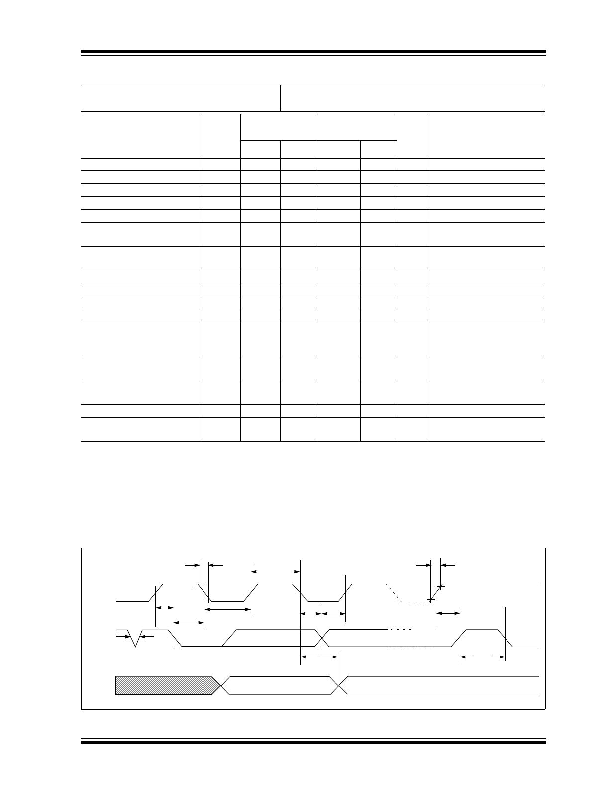
The following bus protocol has been defined:
• Data transfer may be initiated only when the bus
is not busy.
• During data transfer, the data line must remain
stable whenever the clock line is high. Changes in
the data line while the clock line is high will be
interpreted as a Start or Stop condition.
Accordingly, the following bus conditions have been
defined (Figure 3-1).
3.1
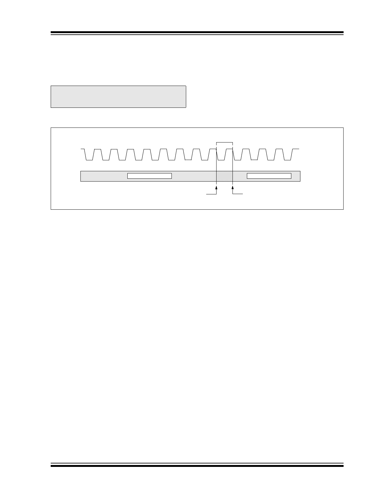
Bus not Busy (A)
Both data and clock lines remain high.
3.2
Start Data Transfer (B)
A high-to-low transition of the SDA line while the clock
(SCL) is high determines a Start condition. All
commands must be preceded by a Start condition.
3.3
Stop Data Transfer (C)
A low-to-high transition of the SDA line while the clock
(SCL) is high determines a Stop condition. All
operations must be ended with a Stop condition.
3.4
Data Valid (D)
The state of the data line represents valid data when,
after a Start condition, the data line is stable for the
duration of the high period of the clock signal.
The data on the line must be changed during the low
period of the clock signal. There is one bit of data per
clock pulse.
Each data transfer is initiated with a Start condition and
terminated with a Stop condition. The number of data
bytes transferred between the Start and Stop
conditions is determined by the master device and is
theoretically unlimited, although only the last sixteen
will be stored when doing a write operation. When an
overwrite does occur it will replace data in a first in first
out fashion.
FIGURE 3-1:
DATA TRANSFER SEQUENCE ON THE SERIAL BUS
(A)
(B)
(D)
(D)
(A)
(C)
SCL
SDA
START
CONDITION
DATA OR
ACKNOWLEDGE
VALID
DATA
ALLOWED
TO CHANGE
STOP
CONDITION
2004 Microchip Technology Inc.
DS21226E-page 5
24LCS61/24LCS62
3.5
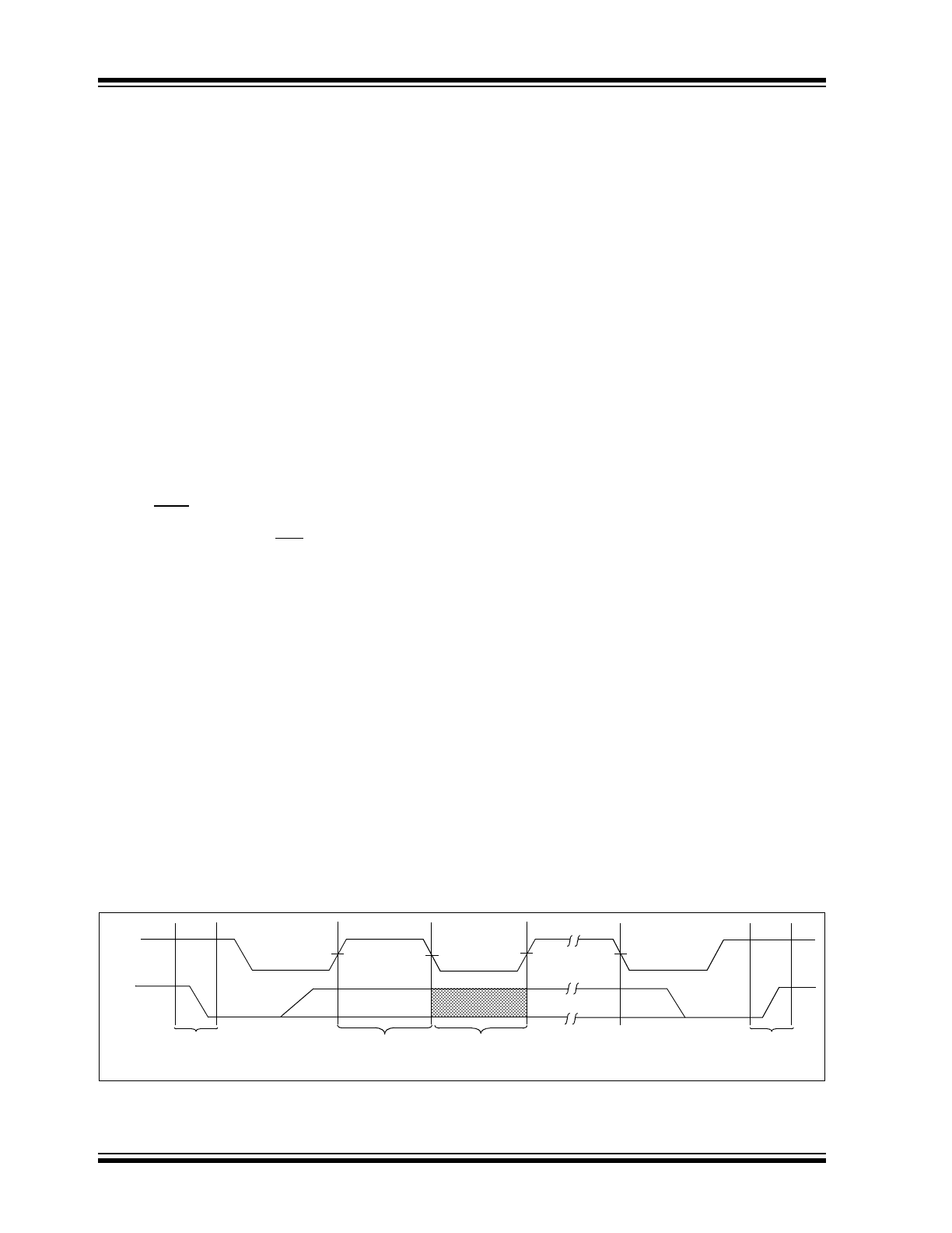
Acknowledge
Each receiving device, when addressed, is required to
generate an acknowledge after the reception of each
byte. The master device must generate an extra clock
pulse which is associated with this Acknowledge bit.
The device that acknowledges has to pull down the
SDA line during the Acknowledge clock pulse in such a
way that the SDA line is stable low during the high
period of the acknowledge related clock pulse. Of
course, setup and hold times must be taken into
account. A master must signal an end of data to the
slave by not generating an Acknowledge bit on the last
byte that has been clocked out of the slave. In this
case, the slave must leave the data line high to enable
the master to generate the Stop condition (Figure 3-2).
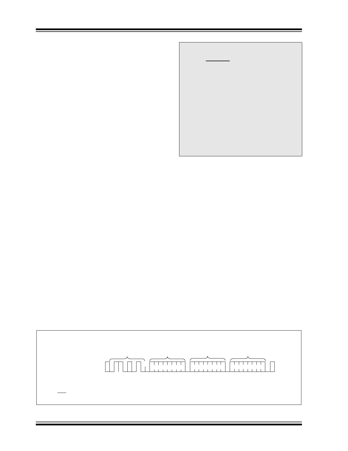
FIGURE 3-2:
ACKNOWLEDGE TIMING
Note:
The 24LCS61/62 does not generate any
Acknowledge bits if an internal program-
ming cycle is in progress.
SCL
9
8
7
6
5
4
3
2
1
1
2
3
Transmitter must release the SDA line at this point
allowing the Receiver to pull the SDA line low to
acknowledge the previous eight bits of data.
Receiver must release the SDA line at this point
so the Transmitter can continue sending data.
Data from transmitter
Data from transmitter
SDA
Acknowledge
Bit
24LCS61/24LCS62
DS21226E-page 6
2004 Microchip Technology Inc.
4.0
FUNCTIONAL DESCRIPTION
The 24LCS61/62 supports a bidirectional 2-wire bus
and data transmission protocol compatible with the I
2
C
protocol. The device is configured to reside on a
common I
2
C bus with up to 255 total 24LCS61/62
devices on the bus. Each device has a unique serial
number assigned to it when delivered from the factory.
In an actual system, this serial number will be used to
assign a separate 8-bit ID byte to each device in the
system. After an ID byte is assigned to each device in
the system, standard Read and Write commands can
be sent to each device individually.
4.1
Device Serial Number
The device serial number is stored in a 48-bit (6 byte)
register that is separate from the data array. The serial
number register is nonvolatile and cannot be changed
by the user. Before shipment from the factory, this
register is programmed with a unique value for every
device. The 48 bit register allows for 2.8
•
10
14
different
combinations. The serial number is used at power-up
to assign the device an ID byte which is then used for
all standard Read and Write commands sent to that
specific device.
4.2
Device ID Byte
The Device ID byte is an 8-bit value that provides the
means for every device on the bus to be accessed
individually. The ID byte is stored in a RAM register
separate from the data array. The ID byte register will
always default to address 00 upon power-up.
4.3
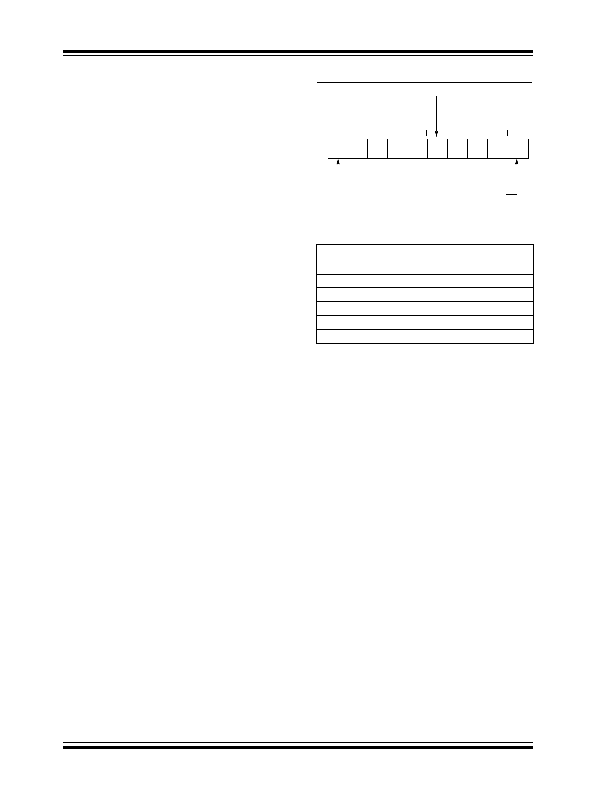
Device Addressing
Each command to the device must begin with a Start
bit. A control byte is the first byte received following the
Start condition from the master device (Figure 4-1).
The control byte consists of a four-bit control code, the
OE bit, and three command select bits. For the
24LCS61/62, the control code is set to ‘
0110
’ binary for
all operations. The device will not acknowledge any
commands sent with any other control code. The next
bit is the Output Enable (OE) bit. This bit controls the
operation of the EDS pin. See Section 9.0 “External
Device Select (EDS) Pin and Output Enable (OE)
Bit” for more details. The last three bits of the control
byte are the command select bits (C0-C2). The
command select bits determine which command will be
executed. See Table 4-1. Following a valid control byte,
the 24LCS61/62 will acknowledge the command.
FIGURE 4-1:
CONTROL BYTE FORMAT
TABLE 4-1:
COMMAND CODES
Command
Command Select Bits
(C2 C1 C0)
Set Write Protection Fuse
000
Read
001
Write (Byte or Page)
010
Assign Address
100
Clear Address
110
1
0
1
0
OE
C2
C1
S
ACK
Control Code
Command Select
Bits
Acknowledge Bit
Start Bit
C0
Output Enable
Bit
2004 Microchip Technology Inc.
DS21226E-page 7
24LCS61/24LCS62
5.0
ASSIGNING THE ID BYTE
The 24LCS61/62 device contains a special register
which holds an 8-bit ID byte that is used as an address
to communicate with a specific device on the bus. All
Read and Write commands to the device must include
this ID address byte. Upon power-up, the ID byte will
default to 00h. Communicating with the device using
the default address is typically done only at testing or
programming time and not when it is connected to a
bus with more than one device. Before the device can
be used on a common bus with other devices, a unique
ID byte address must be assigned to every device.
5.1
Assign Address Command
The ID byte is assigned by sending the Assign Address
command. This command queries any device
connected to the bus and utilizing the automatic bus
arbitration feature, assigns an ID byte to the device that
remains on the bus after arbitration is complete. Once
a device has been assigned an ID byte, it will no longer
respond to Assign Address commands until power is
cycled or the Clear Address command is sent. The
Assign Address command must be repeated for each
device on the bus until all devices have been assigned
an ID byte.
The format for the Assign Address command is shown
in Figure 5-1. The command consists of the control
byte, the ID byte to be assigned to the device remaining
when the arbitration is complete, and 48 bits of data
being transmitted by devices on the bus. If the OE bit is
set to a 1, then any device who has not been assigned
an address will assert their respective EDS pin after the
Acknowledge bit following the Device ID byte. After the
control byte and ID byte are sent, each device will
begin to transmit its unique 48-bit serial number.
The 24LCS61/62 must acknowledge the control byte
and the device ID byte, and the master must acknowl-
edge each byte of the serial number transmitted by the
device. As each bit is clocked out, each device will
monitor the bus to detect if another device is also
transmitting. If any device is outputting a logic ‘1’ on the
bus and it detects that the bus is at a logic ‘0’, then it
assumes that another device is controlling the bus. As
soon as any device detects that it is not controlling the
bus it will immediately stop transmitting data and return
to Standby mode. The master must end the command
by sending a no ACK after all 6 bytes of the serial
number have been transmitted, followed by a Stop bit.
Sending the Stop bit in any other position of the
command will result in the command aborting and all
devices releasing the bus with no address assigned. If
a device transmits its entire 48 bit serial number without
releasing the bus to another device, then the ID byte
transmitted within the command is transferred to the
internal ID byte register upon receipt of the Stop bit and
it will now respond only to commands that contain this
ID byte (or the Clear Address command). Once a
device has been assigned an ID byte, it will no longer
respond to Assign Address commands until power is
cycled or the Clear Address command is sent.
This process of assigning ID bytes is repeated by the
controller until no more devices respond to the Assign
Address command. At this point, all devices on the bus
have been assigned an ID byte and standard Read and
Write commands can be executed to each individual
device.
The ID byte is stored in a volatile SRAM register, and if
power is removed from the device or the Clear Address
command is sent, then the ID byte will default to
address 00 and the process of assigning an ID value
must be repeated.
FIGURE 5-1:
ASSIGN ADDRESS COMMAND
S
P
S
T
A
R
T
CONTROL
BYTE
S
T
O
P
Device ID Byte
6 Bytes (48 Bits) of Device Serial Number
with each byte separated by an ACK bit
1
0
1 0
A unique address must be assigned to each
device on the bus
A
C
K
A
C
K
A
C
K
A
C
K
O
1 0 0
Stop bit must occur here
or command will abort
E
N
O
A
C
K
24LCS61/24LCS62
DS21226E-page 8
2004 Microchip Technology Inc.
5.2
Clear Address Command
The Clear Address command will clear the device ID
byte from all devices on the bus and will enable all
devices to respond to the Assign Address command.
The master must end the command by sending an ACK
after 8 don’t care bits have been transmitted, followed
by a Stop bit. Sending the Stop bit in any other position
of the command will result in the command aborting
and the device releasing the bus.
FIGURE 5-2:
CLEAR ADDRESS COMMAND
5.3
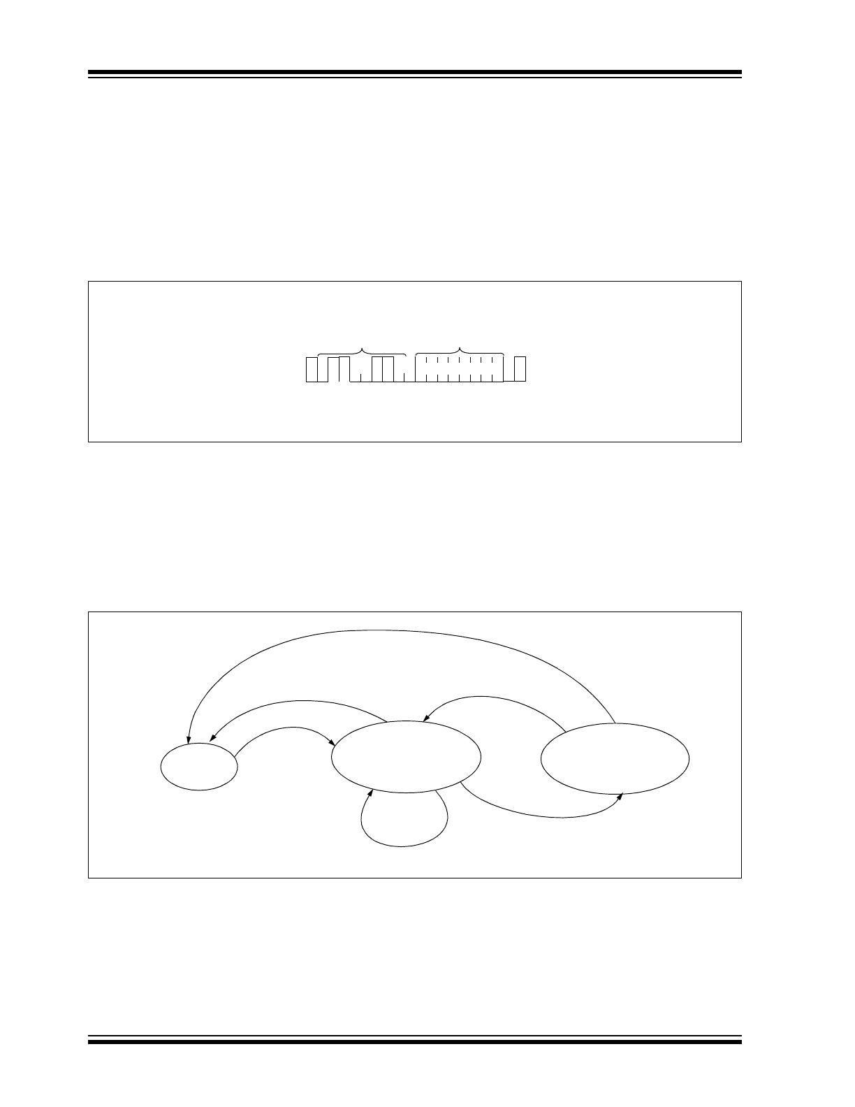
Operation State Diagram
The diagram below shows the state diagram for basic
operation of the 24LCS61/62. This diagram shows
possible states and operational flow once power is
applied to the device. Table 5-1 summarizes operation
of each command for the assigned and unassigned
states.
FIGURE 5-3:
OPERATIONAL STATE DIAGRAM
S
P
S
T
A
R
T
CONTROL
BYTE
S
T
O
P
A
C
K
Device ID Byte
1
0
1 0
A
C
K
X X X X X X X X
0
1 1
O
E
Power
Off
Unassigned
State
Assigned
State
Power Off
Power On
Power Off
Assign Address Command:
Device wins Arbitration
Clear Address
Command
Assign Address Command:
Device loses Arbitration
(ID byte not assigned yet)
(ID byte has been assigned)

2004 Microchip Technology Inc.
DS21226E-page 9
24LCS61/24LCS62
TABLE 5-1:
COMMAND SUMMARY TABLE
Command
Result if Device Has Not Yet
Been Assigned an ID Byte
Result if Device Has Already Been
Assigned an ID Byte
Assign Address
command
If device wins arbitration, then ID
byte will become xxh. If device
loses arbitration, then ID byte will
revert back to 00h.
Device will not acknowledge command.
Clear Address
command
Device will remain with ID byte set
to 00h.
Device ID byte will revert back to 00h and will then
acknowledge Assign Address commands.
Read or Write
command with
ID byte set to 00h
Since the default ID byte for the
device is 00h, the device will
execute the command.
Device will acknowledge the control byte, but it will not
acknowledge any further bytes and will not respond to
the command.
Read or Write
command with
ID byte set to xxh
(other than 00h)
Device will acknowledge the
control byte, but it will not acknowl-
edge any further bytes and will not
respond to the command.
If the device ID byte matches the ID byte in the command
(xxh), the device will execute the command. If the device
ID byte does not match the ID byte in the command, then
the device will acknowledge the control byte, but it will
not acknowledge any further bytes and will not respond
to the command.
Set Write-Protect
command with
ID byte set to 00h
Since the default ID address for the
device is 00h, the device will
execute the command.
Device will acknowledge the control byte, but it will not
acknowledge any further bytes and will not respond to
the command.
Set Write Protection
command with
ID byte set to xxh
(other than 00h)
Device will acknowledge the
control byte, but it will not acknowl-
edge any further bytes and will not
respond to the command.
If the device ID byte matches the ID byte in the command
(xxh), the device will execute the command. If the device
ID byte does not match the ID byte in the command, then
the device will acknowledge the control byte, but it will
not acknowledge any further bytes and will not respond
to the command. Note: Once this command has been
executed successfully for a device, the device will no
longer acknowledge any part of this command again.
24LCS61/24LCS62
DS21226E-page 10
2004 Microchip Technology Inc.
6.0
WRITE OPERATIONS
6.1
Byte Write
Following the Start signal from the master, the control
byte for a Write command is sent by the master
transmitter. The device will acknowledge this control
byte during the ninth clock pulse. The next byte
transmitted by the master is the ID byte for the device.
After receiving another Acknowledge signal from the
24LCS61/62, the master device will transmit the
address and then the data word to be written into the
addressed memory location. The 24LCS61/62
acknowledges between each byte, and the master then
generates a Stop condition. This initiates the internal
write cycle, and during this time the 24LCS61/62 will
not generate Acknowledge signals (Figure 6-1).
6.2
Page Write
The control byte, ID byte, word address, and the first
data byte are transmitted to the 24LCS61/62 in the
same way as in a byte write. But, instead of generating
a Stop condition, the master transmits up to 15
additional data bytes to the 24LCS61/62, which are
temporarily stored in the on-chip page buffer and will be
written into the memory after the master has transmit-
ted a Stop condition. If the master should transmit more
than 16 bytes prior to generating the Stop condition, the
address counter will roll over and the previously
received data will be overwritten. As with the byte write
operation, once the Stop condition is received an
internal write cycle will begin (Figure 6-2) and the
24LCS61/62 will not generate acknowledge.
6.3
Low Voltage Write Protection
The 24LCS61/62 employs a V
CC
threshold detector
circuit which disables the internal erase/write logic, if
the V
CC
is below 1.5 volts at nominal conditions.
6.4
Set Write Protection Command
The Set Write Protection command allows the user to
write-protect a portion of the array. For the 24LCS51
this command will write-protect the entire array. For the
24LCS62 this command will protect the lower half of
the array. This command is illustrated in Figure 6-3.
This is a one time only command and cannot be
reversed once the protection fuse has been set.
Once the write-protect feature has been set, the device
will no longer acknowledge the control byte (or any of
the other bytes) of this command. The Stop bit of this
command initiates an internal write cycle, and during
this time the 24LCS61/62 will not generate
Acknowledge signals.
FIGURE 6-1:
BYTE WRITE
Note:
Page write operations are limited to writing
bytes within a single physical page,
regardless of the number of bytes actually
being written. Physical page boundaries
start at addresses that are integer
multiples of the page buffer size (or ‘page
size’) and end at addresses that are
integer multiples of [page size - 1]. If a
Page Write command attempts to write
across a physical page boundary, the
result is that the data wraps around to the
beginning of the current page (overwriting
data previously stored there), instead of
being written to the next page as might be
expected. It is therefore necessary for the
application software to prevent page write
operations that would attempt to cross a
page boundary.
S
T
A
R
T
S
T
O
P
DEVICE
ID BYTE
DATA
CONTROL
BYTE
A
C
K
A
C
K
A
C
K
BUS ACTIVITY
MASTER
SDA LINE
BUS ACTIVITY
A
C
K
ADDRESS
BYTE
1
0
1 0 O 0 1 0
S
E
OE Bit = EDS Pin Output Enable; see Section 9.0 “External Device Select (EDS) Pin and Output Enable (OE) Bit”
P