
© 2008 Microchip Technology Inc.
DS21160G-page 1
24LC21A
Features:
• Single Supply with Operation Down to 2.5V
• Completely Implements DDC1™/DDC2™
Interface for Monitor Identification, Including
Recovery to DDC1
• Pin and Function Compatible with 24LC21
• Low-Power CMOS Technology
- 1 mA typical active current
- 10
μA standby current typical at 5.5V
• 2-Wire Serial Interface Bus, I
2
C™ Compatible
• 100 kHz (2.5V) and 400 kHz (5V) Compatibility
• Self-Timed Write Cycle (including auto-erase)
• Page Write Buffer for up to Eight Bytes
• 1,000,000 Erase/Write Cycles Ensured
• Data Retention > 200 years
• ESD Protection > 4000V
• 8-pin PDIP and SOIC Package
• Available for Extended Temperature Ranges
• Pb-Free and RoHS Compliant
Description:
The Microchip Technology Inc. 24LC21A is a 128 x 8-bit
dual-mode Electrically Erasable PROM. This device is
designed for use in applications requiring storage and
serial transmission of configuration and control informa-
tion. Two modes of operation have been implemented:
Transmit-Only mode and Bidirectional mode. Upon
power-up, the device will be in the Transmit-Only mode,
sending a serial bit stream of the memory array from 00h
to 7Fh, clocked by the VCLK pin. A valid high-to-low
transition on the SCL pin will cause the device to enter
the transition mode, and look for a valid control byte on
the I
2
C bus. If it detects a valid control byte from the
master, it will switch into Bidirectional mode, with byte
selectable read/write capability of the memory array
using SCL. If no control byte is received, the device will
revert to the Transmit-Only mode after it receives 128
consecutive VCLK pulses while the SCL pin is idle. The
24LC21A is available in a standard 8-pin PDIP and
SOIC package in industrial temperature range.
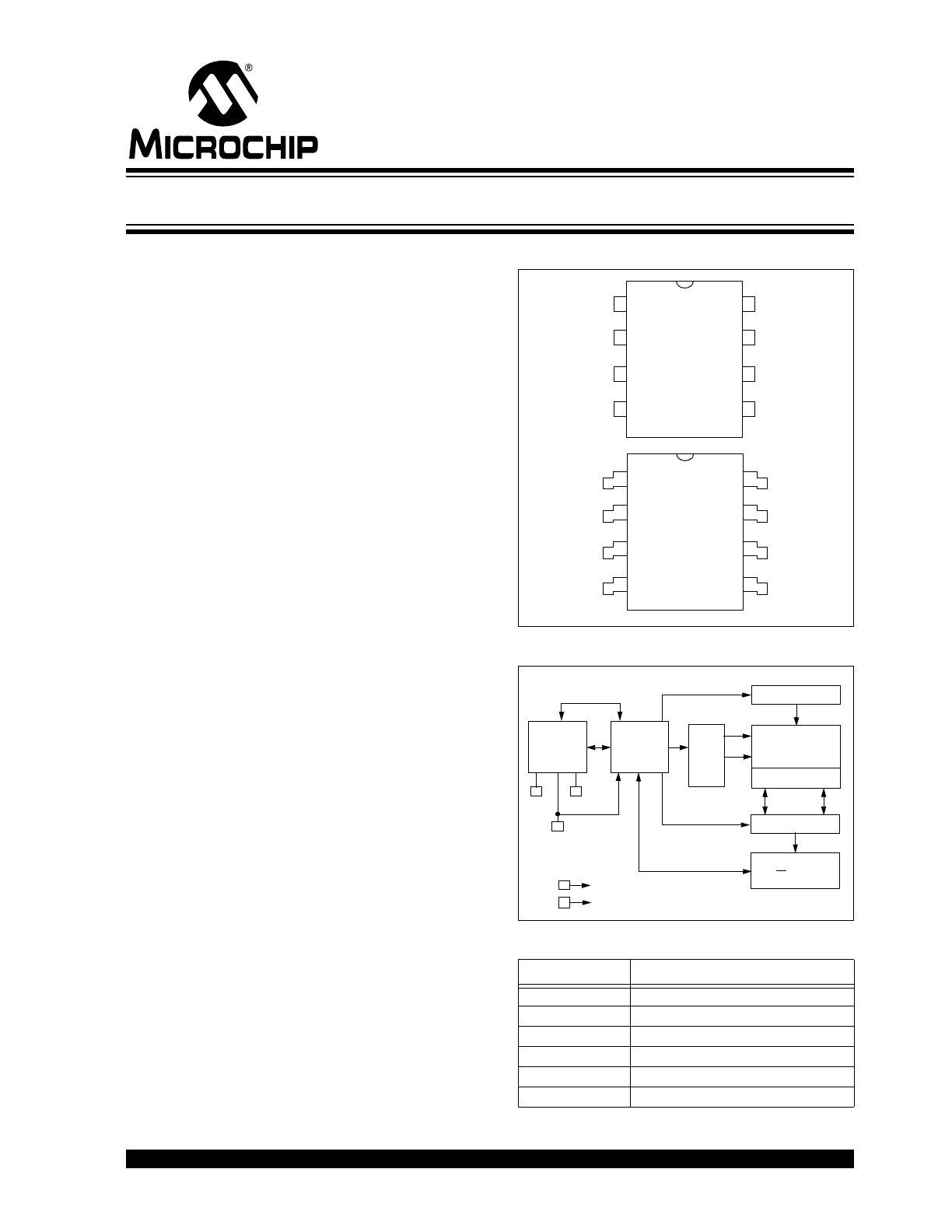
Package Types
Block Diagram
Pin Function Table
- Industrial (I):
-40°C to
+85°C
Name
Function
V
SS
Ground
SDA
Serial Address/Data I/O
SCL
Serial Clock (Bidirectional mode)
VCLK
Serial Clock (Transmit-Only mode)
V
CC
+2.5V to 5.5V Power Supply
NC
No Connection
PDIP
SOIC
24
LC
21
A
NC
NC
NC
V
SS
1
2
3
4
8
7
6
5
Vcc
VCLK
SCL
SDA
24L
C
21A
NC
NC
NC
Vss
1
2
3
4
8
7
6
5
Vcc
VCLK
SCL
SDA
I/O
Control
Logic
HV Generator
EEPROM
Array
Page Latches
YDEC
XDEC
Sense AMP
R/W Control
Memory
Control
Logic
SDA
SCL
V
CC
V
SS
VCLK
1K 2.5V Dual Mode I
2
C
™
Serial EEPROM
DDC is a trademark of the Video Electronics Standards
Association.
I
2
C is a trademark of Philips Corporation.
24LC21A
DS21160G-page 2
© 2008 Microchip Technology Inc.
1.0
ELECTRICAL CHARACTERISTICS
Absolute Maximum Ratings
(†)
V
CC
.............................................................................................................................................................................7.0V
All inputs and outputs w.r.t. V
SS
.........................................................................................................................................-
0.6V to V
CC
+1.0V
Storage temperature ...............................................................................................................................-65
°C to +150°C
Ambient temperature with power applied ................................................................................................-40
°C to +125°C
ESD protection on all pins
......................................................................................................................................................≥ 4 kV
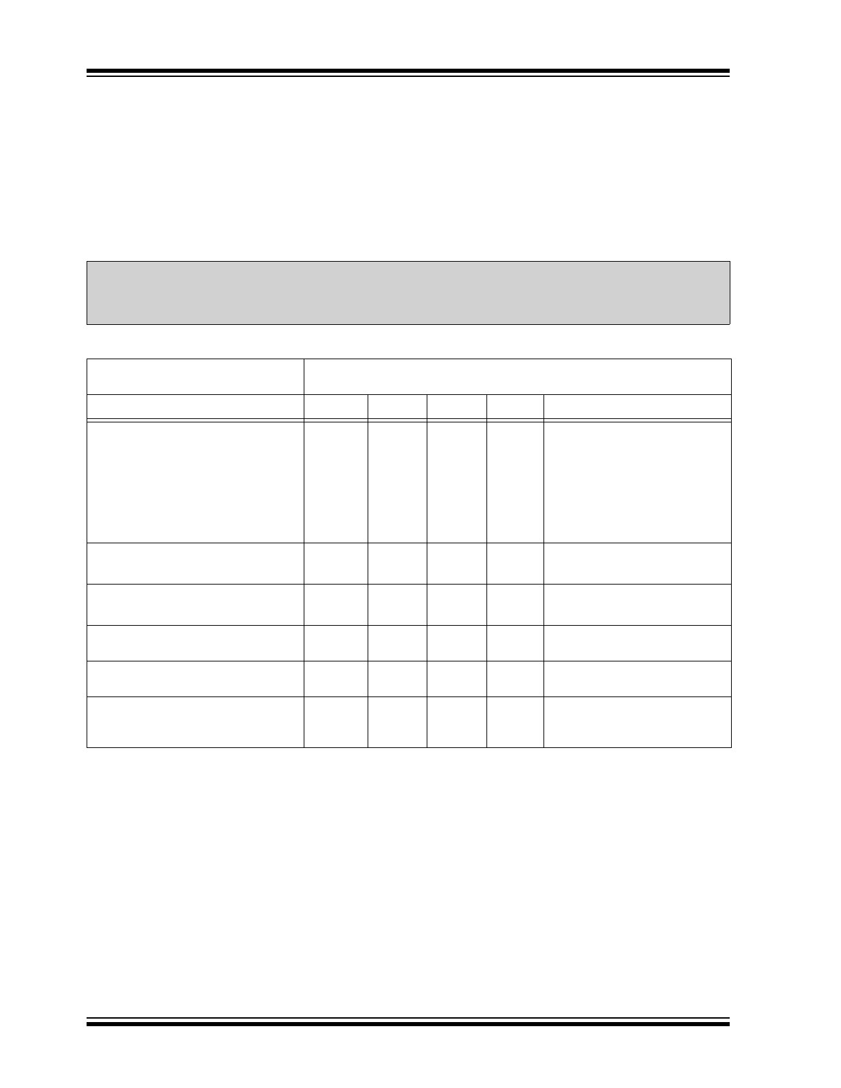
TABLE 1-1:
DC CHARACTERISTICS
† NOTICE: Stresses above those listed under “Absolute Maximum Ratings” may cause permanent damage to
the device. This is a stress rating only and functional operation of the device at those or any other conditions
above those indicated in the operational listings of this specification is not implied. Exposure to maximum rating
conditions for extended periods may affect device reliability.
DC CHARACTERISTICS
V
CC
= +2.5V to 5.5V
Industrial (I):
T
A
=-40
°C to +85°C
Parameter
Symbol
Min.
Max.
Units
Conditions
SCL and SDA pins:
High-level input voltage
Low-level input voltage
V
IH
V
IL
0.7 V
CC
—
—
0.3 V
CC
V
V
Input levels on VCLK pin:
High-level input voltage
Low-level input voltage
V
IH
V
IL
2.0
—
—
0.2 V
CC
V
V
V
CC
≥ 2.7V (Note)
V
CC
< 2.7V (Note)
Hysteresis of Schmitt Trigger inputs
V
HYS
.05 V
CC
—
V
(Note)
Low-level output voltage
V
OL
1
—
0.4
V
I
OL
= 3 mA, V
CC
= 2.5V (Note)
Low-level output voltage
V
OL
2
—
0.6
V
I
OL
= 6 mA, V
CC
= 2.5V
Input leakage current
I
LI
—
±1
μA
V
IN
= 0.1V to V
CC
Output leakage current
I
LO
—
±1
μA
V
OUT
= 0.1V to V
CC
Pin capacitance (all inputs/outputs)
C
IN
, C
OUT
—
10
pF
V
CC
= 5.0V (Note)
T
A
= 25
°C, F
CLK
= 1 MHz
Operating current
I
CC
Write
I
CC
Read
—
—
3
1
mA
mA
V
CC
= 5.5V
V
CC
= 5.5V, SCL = 400 kHz
Standby current
I
CCS
—
—
30
100
μA
μA
V
CC
= 3.0V, SDA = SCL = V
CC
V
CC
= 5.5V, SDA = SCL = V
CC
V
CLK
= V
SS
Note:
This parameter is periodically sampled and not 100% tested.
© 2008 Microchip Technology Inc.
DS21160G-page 3
24LC21A
TABLE 1-2:
AC CHARACTERISTICS
Parameter
Symbol
Vcc = 2.5-5.5V
Standard Mode
Vcc = 4.5 - 5.5V
Fast Mode
Units
Remarks
Min.
Max.
Min.
Max.
Clock frequency
F
CLK
—
100
—
400
kHz
Clock high time
T
HIGH
4000
—
600
—
ns
Clock low time
T
LOW
4700
—
1300
—
ns
SDA and SCL rise time
T
R
—
1000
—
300
ns
(Note 1)
SDA and SCL fall time
T
F
—
300
—
300
ns
(Note 1)
Start condition hold time
T
HD
:
STA
4000
—
600
—
ns
After this period the first clock
pulse is generated
Start condition setup time
T
SU
:
STA
4700
—
600
—
ns
Only relevant for repeated
Start condition
Data input hold time
T
HD
:
DAT
0
—
0
—
ns
(Note 2)
Data input setup time
T
SU
:
DAT
250
—
100
—
ns
Stop condition setup time
T
SU
:
STO
4000
—
600
—
ns
Output valid from clock
T
AA
—
3500
—
900
ns
(Note 2)
Bus free time
T
BUF
4700
—
1300
—
ns
Time the bus must be free
before a new transmission
can start
Output fall time from V
IH
minimum to V
IL
maximum
T
OF
—
250
20 + 0.1
C
B
250
ns
(Note 1), C
B
≤ 100 pF
Input filter spike suppres-
sion (SDA and SCL pins)
T
SP
—
50
—
50
ns
(Note 3)
Write cycle time
T
WR
—
10
—
10
ms
Byte or Page mode
Transmit-Only Mode Parameters
Output valid from VCLK
T
VAA
—
2000
—
1000
ns
VCLK high time
T
VHIGH
4000
—
600
—
ns
VCLK low time
T
VLOW
4700
—
1300
—
ns
VCLK setup time
T
VHST
0
—
0
—
ns
VCLK hold time
T
SPVL
4000
—
600
—
ns
Mode transition time
T
VHZ
—
1000
—
500
ns
Transmit-only power-up
time
T
VPU
0
—
0
—
ns
Input filter spike suppres-
sion (VCLK pin)
T
SPV
—
100
—
100
ns
Endurance
—
1M
—
1M
—
cycles
25°C, Vcc = 5.0V, Block
mode (Note 4)
Note 1:
Not 100% tested. C
B
= Total capacitance of one bus line in pF.
2:
As a transmitter, the device must provide an internal minimum delay time to bridge the undefined region
(minimum 300 ns) of the falling edge of SCL to avoid unintended generation of Start or Stop conditions.
3:
The combined T
SP
and V
HYS
specifications are due to Schmitt Trigger inputs which provide noise and
spike suppression. This eliminates the need for a T
I
specification for standard operation.
4:
This parameter is not tested but ensured by characterization. For endurance estimates in a specific
application, please consult the Total Endurance™ Model which can be obtained from Microchip’s web site
at www.microchip.com.
24LC21A
DS21160G-page 4
© 2008 Microchip Technology Inc.
2.0
FUNCTIONAL DESCRIPTION
The 24LC21A is designed to comply to the DDC
Standard proposed by VESA (Figure 3-3) with the
exception that it is not Access.bus capable. It operates
in two modes, the Transmit-Only mode and the
Bidirectional mode. There is a separate 2-wire protocol
to support each mode, each having a separate clock
input but sharing a common data line (SDA). The
device enters the Transmit-Only mode upon power-up.
In this mode, the device transmits data bits on the SDA
pin in response to a clock signal on the VCLK pin. The
device will remain in this mode until a valid high-to-low
transition is placed on the SCL input. When a valid
transition on SCL is recognized, the device will switch
into the Bidirectional mode and look for its control byte
to be sent by the master. If it detects its control byte, it
will stay in the Bidirectional mode. Otherwise, it will
revert to the Transmit-Only mode after it sees 128
VCLK pulses.
2.1
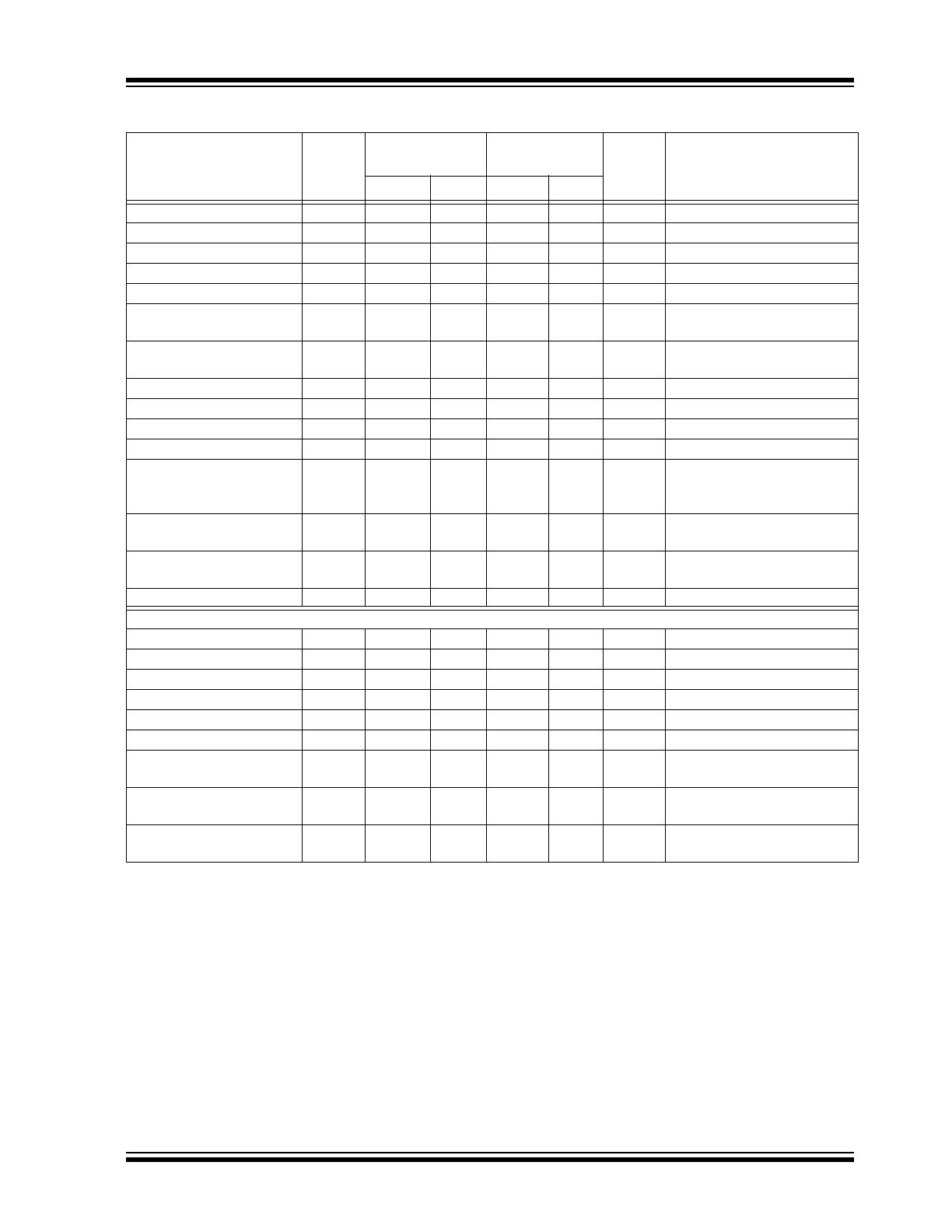
Transmit-Only Mode
The device will power-up in the Transmit-Only mode at
address 00h. This mode supports a unidirectional
2-wire protocol for continuous transmission of the
contents of the memory array. This device requires that
it be initialized prior to valid data being sent in the
Transmit-Only mode (Section 2.2 “Initialization Pro-
cedure”). In this mode, data is transmitted on the SDA
pin in 8-bit bytes, with each byte followed by a ninth,
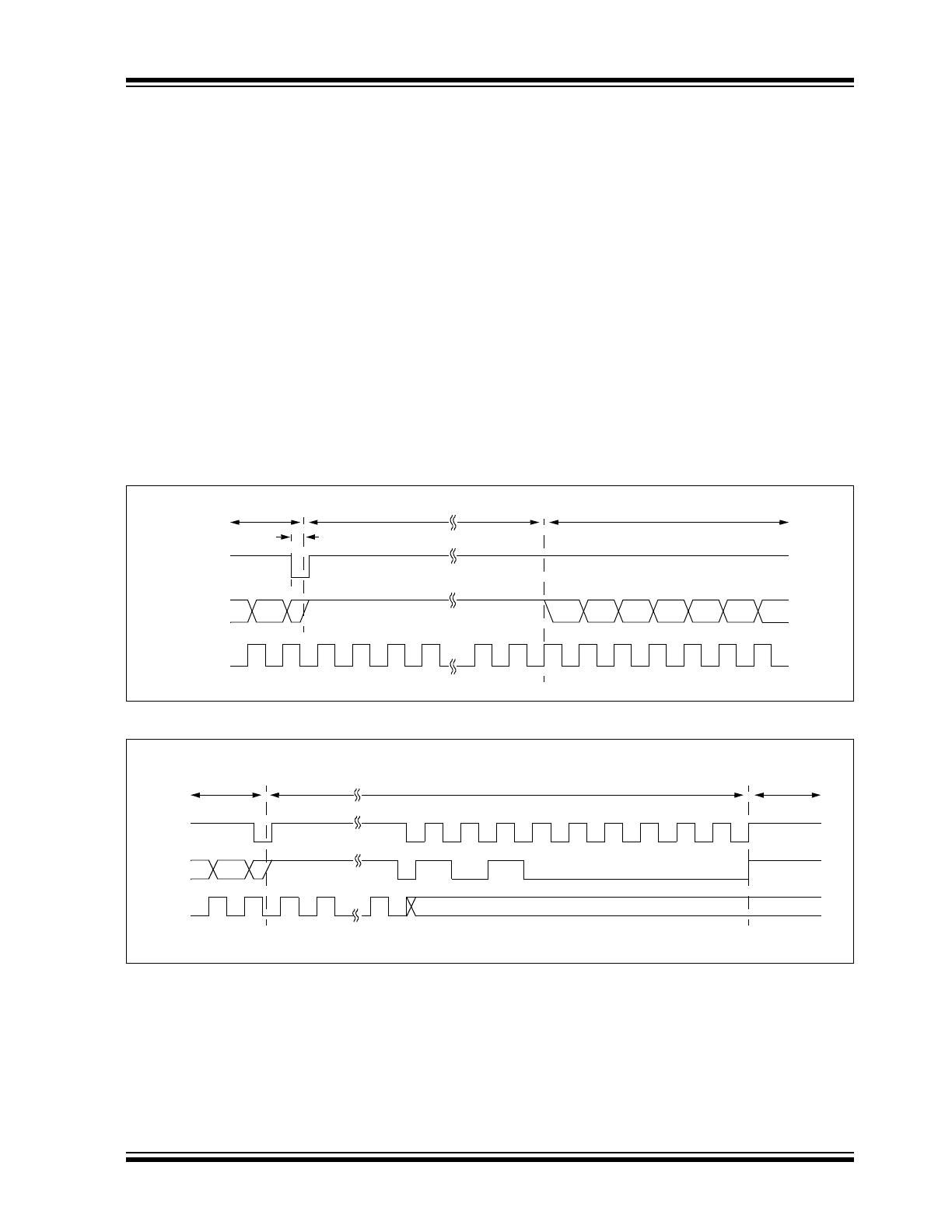
null bit (Figure 2-1). The clock source for the Transmit-
Only mode is provided on the VCLK pin, and a data bit
is output on the rising edge on this pin. The eight bits in
each byte are transmitted Most Significant bit first.
Each byte within the memory array will be output in
sequence. After address 7Fh in the memory array is
transmitted, the internal Address Pointers will wrap
around to the first memory location (00h) and continue.
The Bidirectional mode Clock (SCL) pin must be held
high for the device to remain in the Transmit-Only
mode.
2.2
Initialization Procedure
After V
CC
has stabilized, the device will be in the Trans-
mit-Only mode. Nine clock cycles on the VCLK pin
must be given to the device for it to perform internal
sychronization. During this period, the SDA pin will be
in a high-impedance state. On the rising edge of the
tenth clock cycle, the device will output the first valid
data bit which will be the Most Significant bit in address
00h. (Figure 2-2).
FIGURE 2-1:
TRANSMIT-ONLY MODE
FIGURE 2-2:
DEVICE INITIALIZATION
SCL
SDA
VCLK
Tvaa
Tvaa
Bit 1 (LSB)
Null Bit
Bit 1 (MSB)
Bit 7
Tvlow
Tvhigh
Tvaa
Tvaa
Bit 8
Bit 7
High-Impedance for 9 Clock Cycles
Tvpu
1
2
8
9
10
11
SCL
SDA
VCLK
Vcc
© 2008 Microchip Technology Inc.
DS21160G-page 5
24LC21A
3.0
BIDIRECTIONAL MODE
Before the 24LC21A can be switched into the
Bidirectional mode (Figure 3-1), it must enter the
Transition mode, which is done by applying a valid
high-to-low transition on the Bidirectional mode clock
(SCL). As soon it enters the Transition mode, it looks
for a control byte ‘1010 000X’ on the I
2
C™ bus, and
starts to count pulses on VCLK. Any high-to-low transi-
tion on the SCL line will reset the count. If it sees a
pulse count of 128 on VCLK while the SCL line is idle,
it will revert back to the Transmit-Only mode, and
transmit its contents starting with the Most Significant
bit in address 00h. However, if it detects the control
byte on the I
2
C™ bus, (Figure 3-2) it will switch to the
in the Bidirectional mode. Once the device has made
the transition to the Bidirectional mode, the only way to
switch the device back to the Transmit-Only mode is to
remove power from the device. The mode transition
process is shown in detail in Figure 3-3.
Once the device has switched into the Bidirectional
mode, the VCLK input is disregarded, with the
exception that a logic high level is required to enable
write capability. This mode supports a two-wire
Bidirectional data transmission protocol (I
2
C™). In this
protocol, a device that sends data on the bus is defined
to be the transmitter, and a device that receives data
from the bus is defined to be the receiver. The bus must
be controlled by a master device that generates the
Bidirectional mode clock (SCL), controls access to the
bus and generates the Start and Stop conditions, while
the 24LC21A acts as the slave. Both master and slave
can operate as transmitter or receiver, but the master
device determines which mode is activated. In the
Bidirectional mode, the 24LC21A only responds to
commands for device ‘1010 000X’.
FIGURE 3-1:
MODE TRANSITION WITH RECOVERY TO TRANSMIT-ONLY MODE
FIGURE 3-2:
SUCCESSFUL MODE TRANSITION TO BIDIRECTIONAL MODE
TVHZ
SCL
SDA
VCLK
Transmit-Only
MODE
Bidirectional
Recovery to Transmit-Only mode
Bit 8
(MSB of data in 00h)
VCLK count =
1 2 3 4 127 128
Transition mode with possibility to return to Transmit-Only mode
Bidirectional
permanently
SCL
SDA
VCLK count = 1 2 n 0
VCLK
Transmit-Only
MODE
S
1
0
1
0
0
0
0
0
ACK
n < 128
24LC21A
DS21160G-page 6
© 2008 Microchip Technology Inc.
FIGURE 3-3:
DISPLAY OPERATION PER DDC
STANDARD PROPOSED BY VESA
®
Communication
is idle
Is Vsync
present?
No
Send EDID continuously
using Vsync as clock
High-to-Low
transition on
SCL?
No
Yes
Yes
Stop sending EDID.
Switch to DDC2™ mode.
Display has
transition state
?
optional
Set Vsync counter = 0
Change on
VCLK lines?
SCL, SDA or
No
Yes
High-Low
transition on SCL
?
Reset Vsync counter = 0
No
Yes
Valid
received?
DDC2 address
No
No
VCLK
cycle?
Yes
Increment VCLK counter
Yes
Switch back to DDC1™
mode.
DDC2 communication
idle. Display waiting for
address byte.
DDC2B
address
received?
Yes
Receive DDC2B
command
Respond to DDC2B
command
Is display
Access.bus
TM
Yes
Valid Access.bus
address?
No
Yes
See Access.bus
specification to determine
correct procedure.
Yes
No
Yes
No
No
No
The 24LC21A was designed to
Display Power-on
or
DDC Circuit Powered
from +5 volts
or start timer
Reset counter or timer
(if appropriate)
Counter=128 or
timer expired?
High-to-Low
transition on
SCL?
No
Yes
comply to the portion of flowchart inside dash box
Note 1: The base flowchart is copyright
© 1993, 1994, 1995 Video Electronic Standard Association (VESA) from
VESA’s Display Data Channel (DDC) Standard Proposal ver. 2p rev. 0, used by permission of VESA.
2: The dash box and text “The 24LC21A and... inside dash box.” are added by Microchip Technology Inc.
3: Vsync signal is normally used to derive a signal for VCLK pin on the 24LC21A.
capable?
© 2008 Microchip Technology Inc.
DS21160G-page 7
24LC21A
3.1
Bidirectional Mode Bus
Characteristics
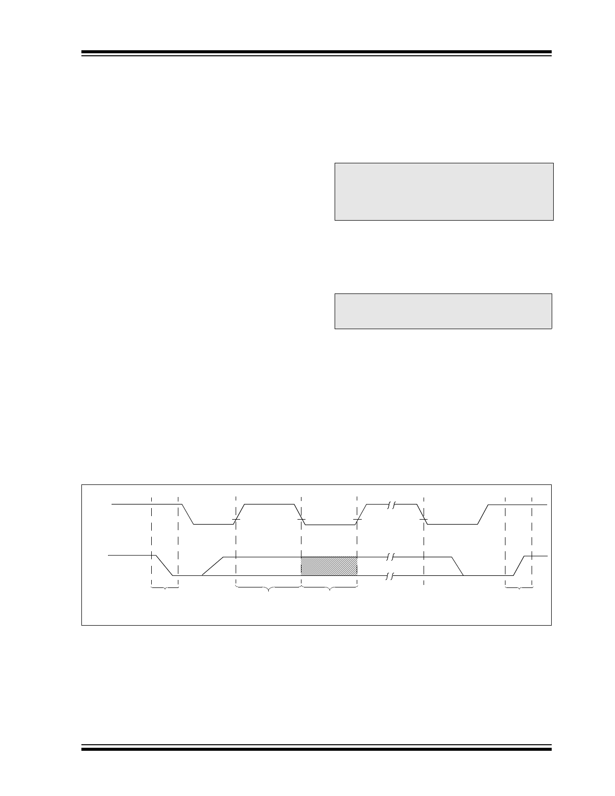
The following bus protocol has been defined:
• Data transfer may be initiated only when the bus
is not busy.
• During data transfer, the data line must remain
stable whenever the clock line is high. Changes in
the data line while the clock line is high will be
interpreted as a Start or Stop condition.
Accordingly, the following bus conditions have been
defined (Figure 3-4).
3.1.1
BUS NOT BUSY (A)
Both data and clock lines remain high.
3.1.2
START DATA TRANSFER (B)
A high-to-low transition of the SDA line while the clock
(SCL) is high determines a Start condition. All
commands must be preceded by a Start condition.
3.1.3
STOP DATA TRANSFER (C)
A low-to-high transition of the SDA line while the clock
(SCL) is high determines a Stop condition. All
operations must be ended with a Stop condition.
3.1.4
DATA VALID (D)
The state of the data line represents valid data when,
after a Start condition, the data line is stable for the
duration of the high period of the clock signal.
The data on the line must be changed during the low
period of the clock signal. There is one clock pulse per
bit of data.
Each data transfer is initiated with a Start condition and
terminated with a Stop condition. The number of the
data bytes transferred between the Start and Stop
conditions is determined by the master device and is
theoretically unlimited, although only the last eight will
be stored when doing a write operation. When an
overwrite does occur it will replace data in a first-in first-
out (FIFO) fashion.
3.1.5
ACKNOWLEDGE
Each receiving device, when addressed, is obliged to
generate an acknowledge after the reception of each
byte. The master device must generate an extra clock
pulse which is associated with this Acknowledge bit.
The device that acknowledges has to pull down the
SDA line during the acknowledge clock pulse in such a
way that the SDA line is stable low during the high
period of the acknowledge related clock pulse. Of
course, setup and hold times must be taken into
account. A master must signal an end of data to the
slave by not generating an Acknowledge bit on the last
byte that has been clocked out of the slave. In this
case, the slave must leave the data line high to enable
the master to generate the Stop condition.
FIGURE 3-4:
DATA TRANSFER SEQUENCE ON THE SERIAL BUS
Note:
Once switched into Bidirectional mode, the
24LC21A will remain in that mode until
power is removed. Removing power is the
only way to reset the 24LC21A into the
Transmit-Only mode.
Note:
The 24LC21A does not generate any
Acknowledge bits if an internal
programming cycle is in progress.
(A)
(B)
(D)
(D)
(A)
(C)
Start
Condition
Address or
Acknowledge
Valid
Data
Allowed
to Change
Stop
Condition
SCL
SDA
24LC21A
DS21160G-page 8
© 2008 Microchip Technology Inc.
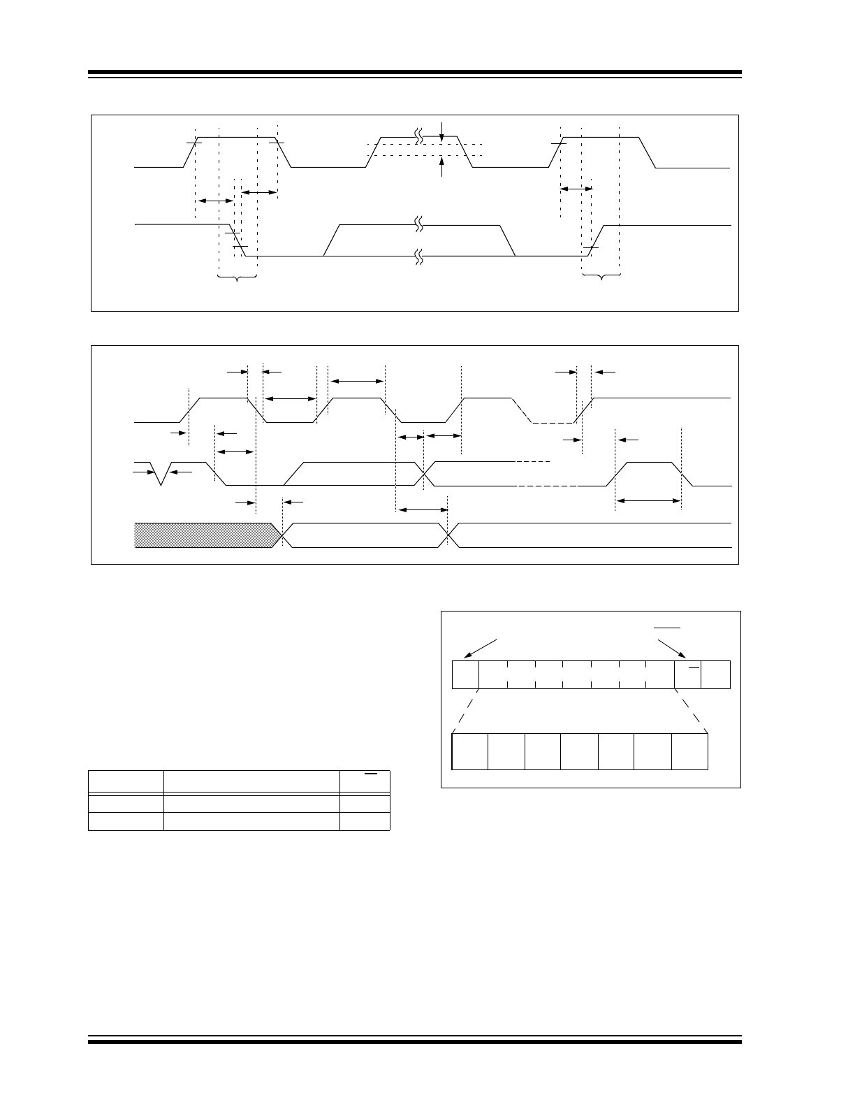
FIGURE 3-5:
BUS TIMING START/STOP
FIGURE 3-6:
BUS TIMING DATA
3.1.6
SLAVE ADDRESS
After generating a Start condition, the bus master
transmits the slave address consisting of a 7-bit device
code (1010000) for the 24LC21A.
The eighth bit of slave address determines whether the
master device wants to read or write to the 24LC21A
(Figure 3-7).
The 24LC21A monitors the bus for its corresponding
slave address continuously. It generates an
Acknowledge bit if the slave address was true and it is
not in a programming mode.
FIGURE 3-7:
CONTROL BYTE
ALLOCATION
SCL
SDA
Start
Stop
V
HYS
T
SU
:
STO
T
HD
:
STA
T
SU
:
STA
SCL
SDA
IN
SDA
OUT
T
SU
:
STA
T
SP
T
AA
T
F
T
LOW
T
HIGH
T
HD
:
STA
T
HD
:
DAT
T
SU
:
DAT
T
SU
:
STO
T
BUF
T
AA
T
R
Operation
Slave Address
R/W
Read
1010000
1
Write
1010000
0
R/W
A
1
0
1
0
0
0
0
Read/Write
Start
Slave Address

© 2008 Microchip Technology Inc.
DS21160G-page 9
24LC21A
4.0
WRITE OPERATION
4.1
Byte Write
Following the start signal from the master, the slave
address (four bits), three zero bits (000) and the R/W
bit which is a logic low are placed onto the bus by the
master transmitter. This indicates to the addressed
slave receiver that a byte with a word address will
follow after it has generated an Acknowledge bit during
the ninth clock cycle. Therefore, the next byte
transmitted by the master is the word address and will
be written into the Address Pointer of the 24LC21A.
After receiving another acknowledge signal from the
24LC21A the master device will transmit the data word
to be written into the addressed memory location. The
24LC21A acknowledges again and the master
generates a Stop condition. This initiates the internal
write cycle, and during this time the 24LC21A will not
generate acknowledge signals (Figure 4-1).
It is required that VCLK be held at a logic high level
during command and data transfer in order to program
the device. This applies to both byte write and page
write operation. Note, however, that the VCLK is
ignored during the self-timed program operation.
Changing VCLK from high-to-low during the self-timed
program operation will not halt programming of the
device.
4.2
Page Write
The write control byte, word address and the first data
byte are transmitted to the 24LC21A in the same way
as in a byte write. But instead of generating a Stop
condition the master transmits up to eight data bytes to
the 24LC21A which are temporarily stored in the on-
chip page buffer and will be written into the memory
after the master has transmitted a Stop condition. After
the receipt of each word, the three lower order Address
Pointer bits are internally incremented by one. The
higher order five bits of the word address remains
constant. If the master should transmit more than eight
words prior to generating the Stop condition, the
address counter will roll over and the previously
received data will be overwritten. As with the byte write
operation, once the Stop condition is received an
internal write cycle will begin (Figure 4-3).
It is required that VCLK be held at a logic high level
during command and data transfer in order to program
the device. This applies to both byte write and page
write operation. Note, however, that the VCLK is
ignored during the self-timed program operation.
Changing VCLK from high-to-low during the self-timed
program operation will not halt programming of the
device.
Note:
Page write operations are limited to writing
bytes within a single physical page,
regardless of the number of bytes actually
being written. Physical page boundaries
start at addresses that are integer multi-
ples of the page buffer size (or ‘page size’)
and end at addresses that are integer
multiples of [page size – 1]. If a Page Write
command attempts to write across a
physical page boundary, the result is that
the data wraps around to the beginning of
the current page (overwriting data
previously stored there), instead of being
written to the next page as might be
expected. It is therefore necessary for the
application software to prevent page write
operations that would attempt to cross a
page boundary.
24LC21A
DS21160G-page 10
© 2008 Microchip Technology Inc.
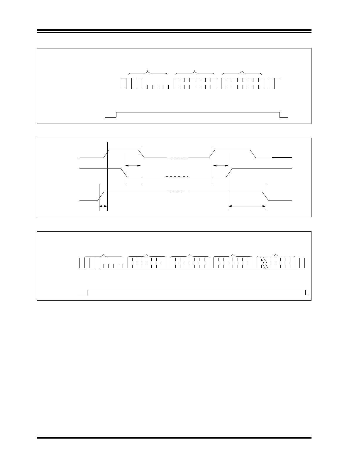
FIGURE 4-1:
BYTE WRITE
FIGURE 4-2:
VCLK WRITE ENABLE TIMING
FIGURE 4-3:
PAGE WRITE
Bus Activity
Master
SDA Line
Bus Activity
Control
Byte
Word
Address
Data
S
T
O
P
S
T
A
R
T
A
C
K
S
P
A
C
K
A
C
K
VCLK
SCL
SDA
IN
VCLK
T
HD
:
STA
T
HD
:
STO
T
VHST
T
SPVL
SDA Line
Control
Byte
Word
Address
S
T
O
P
S
T
A
R
T
A
C
K
A
C
K
A
C
K
A
C
K
A
C
K
Data n + 1
Data n + 7
Data (n)
P
S
VCLK
Bus Activity
Master
Bus Activity
© 2008 Microchip Technology Inc.
DS21160G-page 1
24LC21A
Features:
• Single Supply with Operation Down to 2.5V
• Completely Implements DDC1™/DDC2™
Interface for Monitor Identification, Including
Recovery to DDC1
• Pin and Function Compatible with 24LC21
• Low-Power CMOS Technology
- 1 mA typical active current
- 10
μA standby current typical at 5.5V
• 2-Wire Serial Interface Bus, I
2
C™ Compatible
• 100 kHz (2.5V) and 400 kHz (5V) Compatibility
• Self-Timed Write Cycle (including auto-erase)
• Page Write Buffer for up to Eight Bytes
• 1,000,000 Erase/Write Cycles Ensured
• Data Retention > 200 years
• ESD Protection > 4000V
• 8-pin PDIP and SOIC Package
• Available for Extended Temperature Ranges
• Pb-Free and RoHS Compliant
Description:
The Microchip Technology Inc. 24LC21A is a 128 x 8-bit
dual-mode Electrically Erasable PROM. This device is
designed for use in applications requiring storage and
serial transmission of configuration and control informa-
tion. Two modes of operation have been implemented:
Transmit-Only mode and Bidirectional mode. Upon
power-up, the device will be in the Transmit-Only mode,
sending a serial bit stream of the memory array from 00h
to 7Fh, clocked by the VCLK pin. A valid high-to-low
transition on the SCL pin will cause the device to enter
the transition mode, and look for a valid control byte on
the I
2
C bus. If it detects a valid control byte from the
master, it will switch into Bidirectional mode, with byte
selectable read/write capability of the memory array
using SCL. If no control byte is received, the device will
revert to the Transmit-Only mode after it receives 128
consecutive VCLK pulses while the SCL pin is idle. The
24LC21A is available in a standard 8-pin PDIP and
SOIC package in industrial temperature range.
Package Types
Block Diagram
Pin Function Table
- Industrial (I):
-40°C to
+85°C
Name
Function
V
SS
Ground
SDA
Serial Address/Data I/O
SCL
Serial Clock (Bidirectional mode)
VCLK
Serial Clock (Transmit-Only mode)
V
CC
+2.5V to 5.5V Power Supply
NC
No Connection
PDIP
SOIC
24
LC
21
A
NC
NC
NC
V
SS
1
2
3
4
8
7
6
5
Vcc
VCLK
SCL
SDA
24L
C
21A
NC
NC
NC
Vss
1
2
3
4
8
7
6
5
Vcc
VCLK
SCL
SDA
I/O
Control
Logic
HV Generator
EEPROM
Array
Page Latches
YDEC
XDEC
Sense AMP
R/W Control
Memory
Control
Logic
SDA
SCL
V
CC
V
SS
VCLK
1K 2.5V Dual Mode I
2
C
™
Serial EEPROM
DDC is a trademark of the Video Electronics Standards
Association.
I
2
C is a trademark of Philips Corporation.
24LC21A
DS21160G-page 2
© 2008 Microchip Technology Inc.
1.0
ELECTRICAL CHARACTERISTICS
Absolute Maximum Ratings
(†)
V
CC
.............................................................................................................................................................................7.0V
All inputs and outputs w.r.t. V
SS
.........................................................................................................................................-
0.6V to V
CC
+1.0V
Storage temperature ...............................................................................................................................-65
°C to +150°C
Ambient temperature with power applied ................................................................................................-40
°C to +125°C
ESD protection on all pins
......................................................................................................................................................≥ 4 kV
TABLE 1-1:
DC CHARACTERISTICS
† NOTICE: Stresses above those listed under “Absolute Maximum Ratings” may cause permanent damage to
the device. This is a stress rating only and functional operation of the device at those or any other conditions
above those indicated in the operational listings of this specification is not implied. Exposure to maximum rating
conditions for extended periods may affect device reliability.
DC CHARACTERISTICS
V
CC
= +2.5V to 5.5V
Industrial (I):
T
A
=-40
°C to +85°C
Parameter
Symbol
Min.
Max.
Units
Conditions
SCL and SDA pins:
High-level input voltage
Low-level input voltage
V
IH
V
IL
0.7 V
CC
—
—
0.3 V
CC
V
V
Input levels on VCLK pin:
High-level input voltage
Low-level input voltage
V
IH
V
IL
2.0
—
—
0.2 V
CC
V
V
V
CC
≥ 2.7V (Note)
V
CC
< 2.7V (Note)
Hysteresis of Schmitt Trigger inputs
V
HYS
.05 V
CC
—
V
(Note)
Low-level output voltage
V
OL
1
—
0.4
V
I
OL
= 3 mA, V
CC
= 2.5V (Note)
Low-level output voltage
V
OL
2
—
0.6
V
I
OL
= 6 mA, V
CC
= 2.5V
Input leakage current
I
LI
—
±1
μA
V
IN
= 0.1V to V
CC
Output leakage current
I
LO
—
±1
μA
V
OUT
= 0.1V to V
CC
Pin capacitance (all inputs/outputs)
C
IN
, C
OUT
—
10
pF
V
CC
= 5.0V (Note)
T
A
= 25
°C, F
CLK
= 1 MHz
Operating current
I
CC
Write
I
CC
Read
—
—
3
1
mA
mA
V
CC
= 5.5V
V
CC
= 5.5V, SCL = 400 kHz
Standby current
I
CCS
—
—
30
100
μA
μA
V
CC
= 3.0V, SDA = SCL = V
CC
V
CC
= 5.5V, SDA = SCL = V
CC
V
CLK
= V
SS
Note:
This parameter is periodically sampled and not 100% tested.
© 2008 Microchip Technology Inc.
DS21160G-page 3
24LC21A
TABLE 1-2:
AC CHARACTERISTICS
Parameter
Symbol
Vcc = 2.5-5.5V
Standard Mode
Vcc = 4.5 - 5.5V
Fast Mode
Units
Remarks
Min.
Max.
Min.
Max.
Clock frequency
F
CLK
—
100
—
400
kHz
Clock high time
T
HIGH
4000
—
600
—
ns
Clock low time
T
LOW
4700
—
1300
—
ns
SDA and SCL rise time
T
R
—
1000
—
300
ns
(Note 1)
SDA and SCL fall time
T
F
—
300
—
300
ns
(Note 1)
Start condition hold time
T
HD
:
STA
4000
—
600
—
ns
After this period the first clock
pulse is generated
Start condition setup time
T
SU
:
STA
4700
—
600
—
ns
Only relevant for repeated
Start condition
Data input hold time
T
HD
:
DAT
0
—
0
—
ns
(Note 2)
Data input setup time
T
SU
:
DAT
250
—
100
—
ns
Stop condition setup time
T
SU
:
STO
4000
—
600
—
ns
Output valid from clock
T
AA
—
3500
—
900
ns
(Note 2)
Bus free time
T
BUF
4700
—
1300
—
ns
Time the bus must be free
before a new transmission
can start
Output fall time from V
IH
minimum to V
IL
maximum
T
OF
—
250
20 + 0.1
C
B
250
ns
(Note 1), C
B
≤ 100 pF
Input filter spike suppres-
sion (SDA and SCL pins)
T
SP
—
50
—
50
ns
(Note 3)
Write cycle time
T
WR
—
10
—
10
ms
Byte or Page mode
Transmit-Only Mode Parameters
Output valid from VCLK
T
VAA
—
2000
—
1000
ns
VCLK high time
T
VHIGH
4000
—
600
—
ns
VCLK low time
T
VLOW
4700
—
1300
—
ns
VCLK setup time
T
VHST
0
—
0
—
ns
VCLK hold time
T
SPVL
4000
—
600
—
ns
Mode transition time
T
VHZ
—
1000
—
500
ns
Transmit-only power-up
time
T
VPU
0
—
0
—
ns
Input filter spike suppres-
sion (VCLK pin)
T
SPV
—
100
—
100
ns
Endurance
—
1M
—
1M
—
cycles
25°C, Vcc = 5.0V, Block
mode (Note 4)
Note 1:
Not 100% tested. C
B
= Total capacitance of one bus line in pF.
2:
As a transmitter, the device must provide an internal minimum delay time to bridge the undefined region
(minimum 300 ns) of the falling edge of SCL to avoid unintended generation of Start or Stop conditions.
3:
The combined T
SP
and V
HYS
specifications are due to Schmitt Trigger inputs which provide noise and
spike suppression. This eliminates the need for a T
I
specification for standard operation.
4:
This parameter is not tested but ensured by characterization. For endurance estimates in a specific
application, please consult the Total Endurance™ Model which can be obtained from Microchip’s web site
at www.microchip.com.
24LC21A
DS21160G-page 4
© 2008 Microchip Technology Inc.
2.0
FUNCTIONAL DESCRIPTION
The 24LC21A is designed to comply to the DDC
Standard proposed by VESA (Figure 3-3) with the
exception that it is not Access.bus capable. It operates
in two modes, the Transmit-Only mode and the
Bidirectional mode. There is a separate 2-wire protocol
to support each mode, each having a separate clock
input but sharing a common data line (SDA). The
device enters the Transmit-Only mode upon power-up.
In this mode, the device transmits data bits on the SDA
pin in response to a clock signal on the VCLK pin. The
device will remain in this mode until a valid high-to-low
transition is placed on the SCL input. When a valid
transition on SCL is recognized, the device will switch
into the Bidirectional mode and look for its control byte
to be sent by the master. If it detects its control byte, it
will stay in the Bidirectional mode. Otherwise, it will
revert to the Transmit-Only mode after it sees 128
VCLK pulses.
2.1
Transmit-Only Mode
The device will power-up in the Transmit-Only mode at
address 00h. This mode supports a unidirectional
2-wire protocol for continuous transmission of the
contents of the memory array. This device requires that
it be initialized prior to valid data being sent in the
Transmit-Only mode (Section 2.2 “Initialization Pro-
cedure”). In this mode, data is transmitted on the SDA
pin in 8-bit bytes, with each byte followed by a ninth,
null bit (Figure 2-1). The clock source for the Transmit-
Only mode is provided on the VCLK pin, and a data bit
is output on the rising edge on this pin. The eight bits in
each byte are transmitted Most Significant bit first.
Each byte within the memory array will be output in
sequence. After address 7Fh in the memory array is
transmitted, the internal Address Pointers will wrap
around to the first memory location (00h) and continue.
The Bidirectional mode Clock (SCL) pin must be held
high for the device to remain in the Transmit-Only
mode.
2.2
Initialization Procedure
After V
CC
has stabilized, the device will be in the Trans-
mit-Only mode. Nine clock cycles on the VCLK pin
must be given to the device for it to perform internal
sychronization. During this period, the SDA pin will be
in a high-impedance state. On the rising edge of the
tenth clock cycle, the device will output the first valid
data bit which will be the Most Significant bit in address
00h. (Figure 2-2).
FIGURE 2-1:
TRANSMIT-ONLY MODE
FIGURE 2-2:
DEVICE INITIALIZATION
SCL
SDA
VCLK
Tvaa
Tvaa
Bit 1 (LSB)
Null Bit
Bit 1 (MSB)
Bit 7
Tvlow
Tvhigh
Tvaa
Tvaa
Bit 8
Bit 7
High-Impedance for 9 Clock Cycles
Tvpu
1
2
8
9
10
11
SCL
SDA
VCLK
Vcc
© 2008 Microchip Technology Inc.
DS21160G-page 5
24LC21A
3.0
BIDIRECTIONAL MODE
Before the 24LC21A can be switched into the
Bidirectional mode (Figure 3-1), it must enter the
Transition mode, which is done by applying a valid
high-to-low transition on the Bidirectional mode clock
(SCL). As soon it enters the Transition mode, it looks
for a control byte ‘1010 000X’ on the I
2
C™ bus, and
starts to count pulses on VCLK. Any high-to-low transi-
tion on the SCL line will reset the count. If it sees a
pulse count of 128 on VCLK while the SCL line is idle,
it will revert back to the Transmit-Only mode, and
transmit its contents starting with the Most Significant
bit in address 00h. However, if it detects the control
byte on the I
2
C™ bus, (Figure 3-2) it will switch to the
in the Bidirectional mode. Once the device has made
the transition to the Bidirectional mode, the only way to
switch the device back to the Transmit-Only mode is to
remove power from the device. The mode transition
process is shown in detail in Figure 3-3.
Once the device has switched into the Bidirectional
mode, the VCLK input is disregarded, with the
exception that a logic high level is required to enable
write capability. This mode supports a two-wire
Bidirectional data transmission protocol (I
2
C™). In this
protocol, a device that sends data on the bus is defined
to be the transmitter, and a device that receives data
from the bus is defined to be the receiver. The bus must
be controlled by a master device that generates the
Bidirectional mode clock (SCL), controls access to the
bus and generates the Start and Stop conditions, while
the 24LC21A acts as the slave. Both master and slave
can operate as transmitter or receiver, but the master
device determines which mode is activated. In the
Bidirectional mode, the 24LC21A only responds to
commands for device ‘1010 000X’.
FIGURE 3-1:
MODE TRANSITION WITH RECOVERY TO TRANSMIT-ONLY MODE
FIGURE 3-2:
SUCCESSFUL MODE TRANSITION TO BIDIRECTIONAL MODE
TVHZ
SCL
SDA
VCLK
Transmit-Only
MODE
Bidirectional
Recovery to Transmit-Only mode
Bit 8
(MSB of data in 00h)
VCLK count =
1 2 3 4 127 128
Transition mode with possibility to return to Transmit-Only mode
Bidirectional
permanently
SCL
SDA
VCLK count = 1 2 n 0
VCLK
Transmit-Only
MODE
S
1
0
1
0
0
0
0
0
ACK
n < 128
24LC21A
DS21160G-page 6
© 2008 Microchip Technology Inc.
FIGURE 3-3:
DISPLAY OPERATION PER DDC
STANDARD PROPOSED BY VESA
®
Communication
is idle
Is Vsync
present?
No
Send EDID continuously
using Vsync as clock
High-to-Low
transition on
SCL?
No
Yes
Yes
Stop sending EDID.
Switch to DDC2™ mode.
Display has
transition state
?
optional
Set Vsync counter = 0
Change on
VCLK lines?
SCL, SDA or
No
Yes
High-Low
transition on SCL
?
Reset Vsync counter = 0
No
Yes
Valid
received?
DDC2 address
No
No
VCLK
cycle?
Yes
Increment VCLK counter
Yes
Switch back to DDC1™
mode.
DDC2 communication
idle. Display waiting for
address byte.
DDC2B
address
received?
Yes
Receive DDC2B
command
Respond to DDC2B
command
Is display
Access.bus
TM
Yes
Valid Access.bus
address?
No
Yes
See Access.bus
specification to determine
correct procedure.
Yes
No
Yes
No
No
No
The 24LC21A was designed to
Display Power-on
or
DDC Circuit Powered
from +5 volts
or start timer
Reset counter or timer
(if appropriate)
Counter=128 or
timer expired?
High-to-Low
transition on
SCL?
No
Yes
comply to the portion of flowchart inside dash box
Note 1: The base flowchart is copyright
© 1993, 1994, 1995 Video Electronic Standard Association (VESA) from
VESA’s Display Data Channel (DDC) Standard Proposal ver. 2p rev. 0, used by permission of VESA.
2: The dash box and text “The 24LC21A and... inside dash box.” are added by Microchip Technology Inc.
3: Vsync signal is normally used to derive a signal for VCLK pin on the 24LC21A.
capable?
© 2008 Microchip Technology Inc.
DS21160G-page 7
24LC21A
3.1
Bidirectional Mode Bus
Characteristics
The following bus protocol has been defined:
• Data transfer may be initiated only when the bus
is not busy.
• During data transfer, the data line must remain
stable whenever the clock line is high. Changes in
the data line while the clock line is high will be
interpreted as a Start or Stop condition.
Accordingly, the following bus conditions have been
defined (Figure 3-4).
3.1.1
BUS NOT BUSY (A)
Both data and clock lines remain high.
3.1.2
START DATA TRANSFER (B)
A high-to-low transition of the SDA line while the clock
(SCL) is high determines a Start condition. All
commands must be preceded by a Start condition.
3.1.3
STOP DATA TRANSFER (C)
A low-to-high transition of the SDA line while the clock
(SCL) is high determines a Stop condition. All
operations must be ended with a Stop condition.
3.1.4
DATA VALID (D)
The state of the data line represents valid data when,
after a Start condition, the data line is stable for the
duration of the high period of the clock signal.
The data on the line must be changed during the low
period of the clock signal. There is one clock pulse per
bit of data.
Each data transfer is initiated with a Start condition and
terminated with a Stop condition. The number of the
data bytes transferred between the Start and Stop
conditions is determined by the master device and is
theoretically unlimited, although only the last eight will
be stored when doing a write operation. When an
overwrite does occur it will replace data in a first-in first-
out (FIFO) fashion.
3.1.5
ACKNOWLEDGE
Each receiving device, when addressed, is obliged to
generate an acknowledge after the reception of each
byte. The master device must generate an extra clock
pulse which is associated with this Acknowledge bit.
The device that acknowledges has to pull down the
SDA line during the acknowledge clock pulse in such a
way that the SDA line is stable low during the high
period of the acknowledge related clock pulse. Of
course, setup and hold times must be taken into
account. A master must signal an end of data to the
slave by not generating an Acknowledge bit on the last
byte that has been clocked out of the slave. In this
case, the slave must leave the data line high to enable
the master to generate the Stop condition.
FIGURE 3-4:
DATA TRANSFER SEQUENCE ON THE SERIAL BUS
Note:
Once switched into Bidirectional mode, the
24LC21A will remain in that mode until
power is removed. Removing power is the
only way to reset the 24LC21A into the
Transmit-Only mode.
Note:
The 24LC21A does not generate any
Acknowledge bits if an internal
programming cycle is in progress.
(A)
(B)
(D)
(D)
(A)
(C)
Start
Condition
Address or
Acknowledge
Valid
Data
Allowed
to Change
Stop
Condition
SCL
SDA
24LC21A
DS21160G-page 8
© 2008 Microchip Technology Inc.
FIGURE 3-5:
BUS TIMING START/STOP
FIGURE 3-6:
BUS TIMING DATA
3.1.6
SLAVE ADDRESS
After generating a Start condition, the bus master
transmits the slave address consisting of a 7-bit device
code (1010000) for the 24LC21A.
The eighth bit of slave address determines whether the
master device wants to read or write to the 24LC21A
(Figure 3-7).
The 24LC21A monitors the bus for its corresponding
slave address continuously. It generates an
Acknowledge bit if the slave address was true and it is
not in a programming mode.
FIGURE 3-7:
CONTROL BYTE
ALLOCATION
SCL
SDA
Start
Stop
V
HYS
T
SU
:
STO
T
HD
:
STA
T
SU
:
STA
SCL
SDA
IN
SDA
OUT
T
SU
:
STA
T
SP
T
AA
T
F
T
LOW
T
HIGH
T
HD
:
STA
T
HD
:
DAT
T
SU
:
DAT
T
SU
:
STO
T
BUF
T
AA
T
R
Operation
Slave Address
R/W
Read
1010000
1
Write
1010000
0
R/W
A
1
0
1
0
0
0
0
Read/Write
Start
Slave Address
© 2008 Microchip Technology Inc.
DS21160G-page 9
24LC21A
4.0
WRITE OPERATION
4.1
Byte Write
Following the start signal from the master, the slave
address (four bits), three zero bits (000) and the R/W
bit which is a logic low are placed onto the bus by the
master transmitter. This indicates to the addressed
slave receiver that a byte with a word address will
follow after it has generated an Acknowledge bit during
the ninth clock cycle. Therefore, the next byte
transmitted by the master is the word address and will
be written into the Address Pointer of the 24LC21A.
After receiving another acknowledge signal from the
24LC21A the master device will transmit the data word
to be written into the addressed memory location. The
24LC21A acknowledges again and the master
generates a Stop condition. This initiates the internal
write cycle, and during this time the 24LC21A will not
generate acknowledge signals (Figure 4-1).
It is required that VCLK be held at a logic high level
during command and data transfer in order to program
the device. This applies to both byte write and page
write operation. Note, however, that the VCLK is
ignored during the self-timed program operation.
Changing VCLK from high-to-low during the self-timed
program operation will not halt programming of the
device.
4.2
Page Write
The write control byte, word address and the first data
byte are transmitted to the 24LC21A in the same way
as in a byte write. But instead of generating a Stop
condition the master transmits up to eight data bytes to
the 24LC21A which are temporarily stored in the on-
chip page buffer and will be written into the memory
after the master has transmitted a Stop condition. After
the receipt of each word, the three lower order Address
Pointer bits are internally incremented by one. The
higher order five bits of the word address remains
constant. If the master should transmit more than eight
words prior to generating the Stop condition, the
address counter will roll over and the previously
received data will be overwritten. As with the byte write
operation, once the Stop condition is received an
internal write cycle will begin (Figure 4-3).
It is required that VCLK be held at a logic high level
during command and data transfer in order to program
the device. This applies to both byte write and page
write operation. Note, however, that the VCLK is
ignored during the self-timed program operation.
Changing VCLK from high-to-low during the self-timed
program operation will not halt programming of the
device.
Note:
Page write operations are limited to writing
bytes within a single physical page,
regardless of the number of bytes actually
being written. Physical page boundaries
start at addresses that are integer multi-
ples of the page buffer size (or ‘page size’)
and end at addresses that are integer
multiples of [page size – 1]. If a Page Write
command attempts to write across a
physical page boundary, the result is that
the data wraps around to the beginning of
the current page (overwriting data
previously stored there), instead of being
written to the next page as might be
expected. It is therefore necessary for the
application software to prevent page write
operations that would attempt to cross a
page boundary.
24LC21A
DS21160G-page 10
© 2008 Microchip Technology Inc.
FIGURE 4-1:
BYTE WRITE
FIGURE 4-2:
VCLK WRITE ENABLE TIMING
FIGURE 4-3:
PAGE WRITE
Bus Activity
Master
SDA Line
Bus Activity
Control
Byte
Word
Address
Data
S
T
O
P
S
T
A
R
T
A
C
K
S
P
A
C
K
A
C
K
VCLK
SCL
SDA
IN
VCLK
T
HD
:
STA
T
HD
:
STO
T
VHST
T
SPVL
SDA Line
Control
Byte
Word
Address
S
T
O
P
S
T
A
R
T
A
C
K
A
C
K
A
C
K
A
C
K
A
C
K
Data n + 1
Data n + 7
Data (n)
P
S
VCLK
Bus Activity
Master
Bus Activity