
2004 Microchip Technology Inc.
DS21126E-page 1
24FC32
Features
• Voltage operating range: 4.5V to 5.5V
- Maximum write current 3 mA at 5.5V
- Maximum read current 150
µ
A at 5.5V
- Standby current 1
µ
A typical
• 1 MHz SE2.bus two wire protocol
• Self-timed write cycle (including auto-erase)
• Power on/off data protection circuitry
• Endurance:
- 10,000,000 Erase/Write cycles ensured for a
4K block
- 1,000,000 E/W cycles ensured for a 28K
block
• 8-byte page, or byte modes available
• 1 page x 8 line input cache (64 bytes) for fast write
loads
• Schmitt Trigger inputs for noise suppression
• 2 ms typical write cycle time, byte or page
• Up to 8 chips may be connected to the same bus
for up to 256K bits total memory
• Electrostatic discharge protection > 4000V
• Data retention > 200 years
• 8-pin PDIP/SOIC packages
• Temperature ranges
Description
The Microchip Technology Inc. 24FC32 is a 4K x 8 (32K
bit) Serial Electrically Erasable PROM (EEPROM) with
a high-speed 1 MHz SE2.bus whose protocol is
functionally equivalent to the industry-standard I
2
C
bus. This device has been developed for advanced,
low power applications such as personal
communications or data acquisition. The 24FC32
features an input cache for fast write loads with a
capacity of eight 8-byte pages, or 64 bytes. It also
features a fixed 4K-bit block of ultra-high endurance
memory for data that changes frequently. The 24FC32
is capable of both random and sequential reads up to
the 32K boundary. Functional address lines allow up to
eight 24FC32 devices on the same bus, for up to 256K
bits address space. The 24FC32 is available in the
standard 8-pin plastic DIP and 8-pin surface mount
SOIC package.
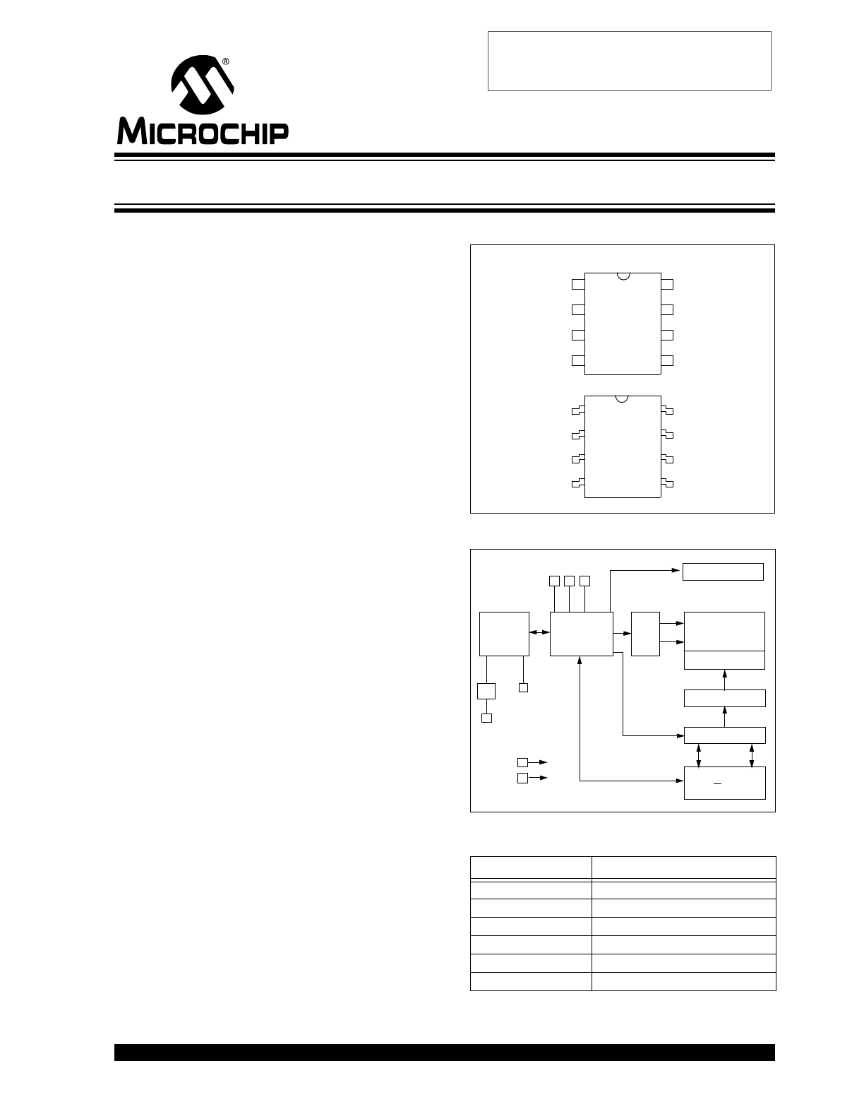
Package Types
Block Diagram
Pin Function Table
- Commercial (C):
0°C
to
+70°C
- Industrial (I):
-40°C
to
+85°C
Name
Function
A0, A1, A2
User Configurable Chip Selects
V
SS
Ground
SDA
Serial Address/Data I/O
SCL
Serial Clock
V
CC
+4.5V to 5.5V Power Supply
NC
No Internal Connection
24F
C
3
2
SOIC
1
2
3
4
8
7
6
5
Vcc
NC
SCL
SDA
A0
A1
A2
Vss
24F
C
3
2
PDIP
1
2
3
4
8
7
6
5
Vcc
NC
SCL
SDA
A0
A1
A2
Vss
HV Generator
EEPROM
Array
Page Latches
YDEC
XDEC
Sense AMP
R/W Control
Memory
Control
Logic
I/O
Control
Logic
SDA
SCL
V
CC
V
SS
I/O
A2
A1
A0
Cache
32K 5.0V 1 MHz I
2
C
™
Smart Serial
™
EEPROM
I
2
C is a trademark of Philips Corporation.
Smart Serial is a trademark of Microchip Technology Inc.
Obsolete Device
Please use 24LC32A or 24LC65.
24FC32
DS21126E-page 2
2004 Microchip Technology Inc.
1.0
ELECTRICAL CHARACTERISTICS
Absolute Maximum Ratings
(†)
V
CC
.............................................................................................................................................................................7.0V
All inputs and outputs w.r.t. V
SS
......................................................................................................... -0.6V to V
CC
+1.0V
Storage temperature ...............................................................................................................................-65°C to +150°C
Ambient temperature with power applied ................................................................................................-65°C to +125°C
ESD protection on all pins
......................................................................................................................................................≥
4 kV
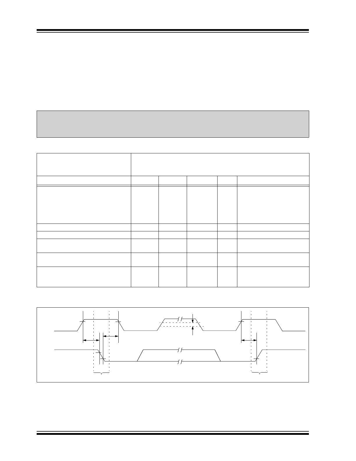
TABLE 1:
DC CHARACTERISTICS
FIGURE 1-1:
BUS TIMING START/STOP
† NOTICE: Stresses above those listed under “Absolute Maximum Ratings” may cause permanent damage to
the device. This is a stress rating only and functional operation of the device at those or any other conditions
above those indicated in the operational listings of this specification is not implied. Exposure to maximum rating
conditions for extended periods may affect device reliability.
DC CHARACTERISTICS
V
CC
= +4.5V to +5.5V
Commercial (C): T
A
= 0°C to +70°C
Industrial (I):
T
A
= -40°C to +85°C
Parameter
Symbol
Min
Max
Units
Conditions
A0, A1, A2, SCL and SDA pins:
High-level input voltage
V
IH
0.7 Vcc
—
V
Low-level input voltage
V
IL
—
0.3 Vcc
V
Hysteresis of SCL and SDA
V
HYS
0.05 Vcc
—
V
(Note)
Low-level output voltage of SDA
V
OL
—
0.40
V
I
OL
= 3.0 mA
Input leakage current
I
LI
—
±1
µ
A
Vin = 0.1V to Vcc
Output leakage current
I
LO
—
±1
µ
A
V
OUT
= 0.1V to V
CC
Pin capacitance
(all inputs/outputs)
C
INT
—
10
pF
V
CC
= 5.0V (Note)
T
A
= 25°C, F
CLK
= 1 MHz
Operating current
Icc Write
I
CC
Read
—
—
3
150
mA
µ
A
V
CC
= 5.5V, SCL = 1 MHz
V
CC
= 5.5V, SCL = 1 MHz
Standby current
I
CCS
—
5
(1 typical)
µ
A
V
CC
= 5.5V,
SCL = SDA = V
CC
A0, A1, A2 = V
SS
Note:
This parameter is periodically sampled and not 100% tested.
T
SU
:
STA
T
HD
:
STA
V
HYS
T
SU
:
STO
START
STOP
SCL
SDA
2004 Microchip Technology Inc.
DS21126E-page 3
24FC32
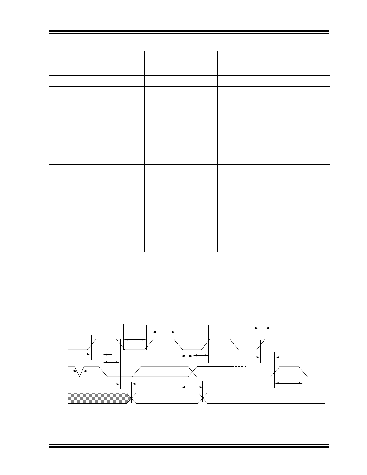
TABLE 1-1:
AC CHARACTERISTICS
FIGURE 1-2:
BUS TIMING DATA
Parameter
Symbol
1 MHz Bus
Units
Remarks
Min
Max
Clock frequency
F
CLK
0
1000
kHz
Clock high time
T
HIGH
500
—
ns
Clock low time
T
LOW
500
—
ns
SDA and SCL rise time
T
R
—
300
ns
(Note 1)
SDA and SCL fall time
T
F
—
100
ns
(Note 1)
Start condition hold time
T
HD
:
STA
250
—
ns
After this period the first clock pulse is
generated
Start condition setup time
T
SU
:
STA
250
—
ns
Only relevant for repeated Start condition
Data input hold time
T
HD
:
DAT
0
—
ns
Data input setup time
T
SU
:
DAT
100
—
ns
Stop condition setup time
T
SU
:
STO
250
—
ns
Output valid from clock
T
AA
—
350
ns
(Note 2)
Bus free time
T
BUF
500
—
ns
Time the bus must be free before a new
transmission can start
Write cycle time
T
WR
—
5
ms/page Note 3
Endurance
High Endurance
Block
Rest of Array
—
—
10M
1M
—
—
10M
1M
25°C, Vcc = 5.0V, Block mode (Note 4)
Note 1:
Not 100 percent tested.
2:
As a transmitter, the device must provide an internal minimum delay time to bridge the undefined region
(minimum 100 ns) of the falling edge of SCL to avoid unintended generation of Start or Stop conditions.
3:
The times shown are for a single page of 8 bytes. Multiply by the number of pages loaded into the write
cache for total time.
4:
This parameter is not tested but ensured by characterization. For endurance estimates in a specific
application, please consult the Total Endurance™ Model which can be obtained from our web site.
SCL
SDA
IN
SDA
OUT
T
SU
:
STA
T
SP
T
AA
T
F
T
LOW
T
HIGH
T
HD
:
STA
T
HD
:
DAT
T
SU
:
DAT
T
SU
:
STO
T
BUF
T
AA
T
R
24FC32
DS21126E-page 4
2004 Microchip Technology Inc.
2.0
FUNCTIONAL DESCRIPTION
The 24FC32 supports a bidirectional two-wire bus and
data transmission protocol. A device that sends data
onto the bus is defined as transmitter, and a device
receiving data as receiver. The bus must be controlled
by a master device which generates the serial clock
(SCL), controls the bus access, and generates the Start
and Stop conditions, while the 24FC32 works as slave.
Both master and slave can operate as transmitter or
receiver but the master device determines which mode
is activated.
3.0
BUS CHARACTERISTICS
The following bus protocol has been defined:
• Data transfer may be initiated only when the bus
is not busy.
• During data transfer, the data line must remain
stable whenever the clock line is high. Changes in
the data line while the clock line is high will be
interpreted as a Start or Stop condition.
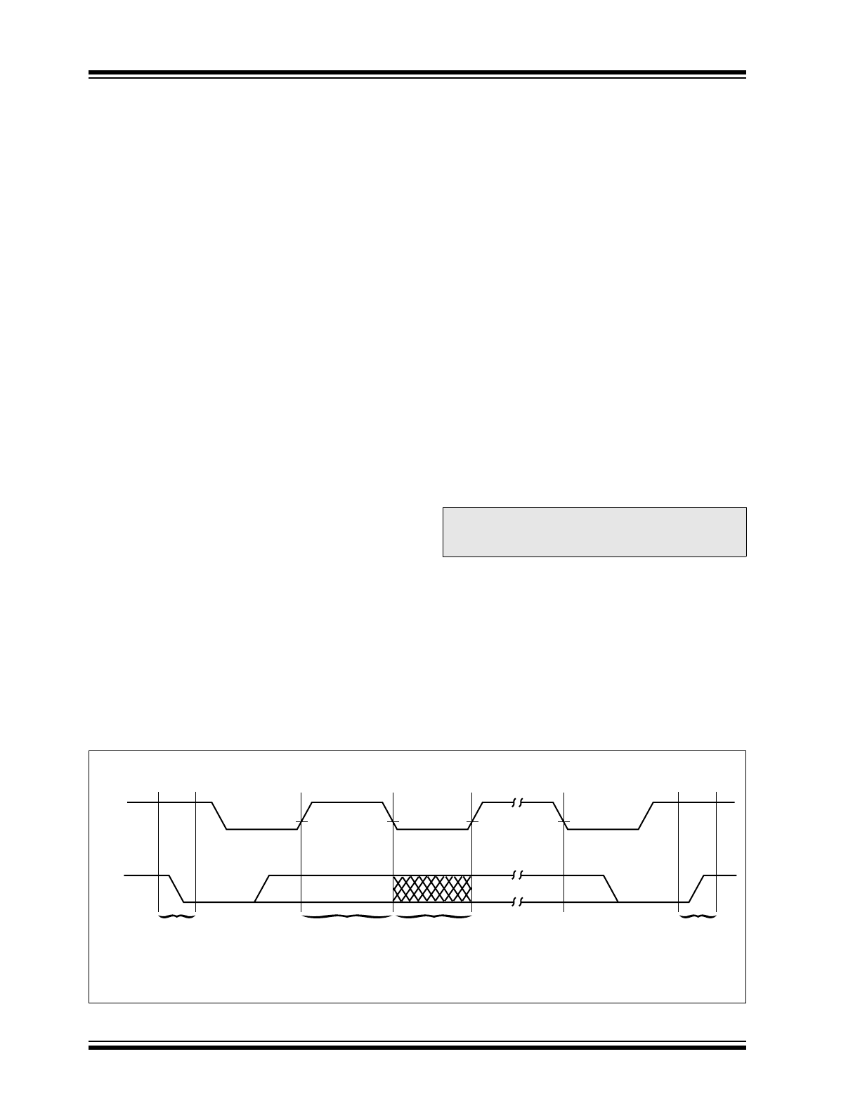
Accordingly, the following bus conditions have been
defined (Figure 3-1).
3.1
Bus not Busy (A)
Both data and clock lines remain high.
3.2
Start Data Transfer (B)
A high-to-low transition of the SDA line while the clock
(SCL) is high determines a Start condition. All
commands must be preceded by a Start condition.
3.3
Stop Data Transfer (C)
A low-to-high transition of the SDA line while the clock
(SCL) is high determines a Stop condition. All
operations must be ended with a Stop condition.
3.4
Data Valid (D)
The state of the data line represents valid data when,
after a Start condition, the data line is stable for the
duration of the high period of the clock signal.
The data on the line must be changed during the low
period of the clock signal. There is one clock pulse per
bit of data.
Each data transfer is initiated with a Start condition and
terminated with a Stop condition. The number of the
data bytes transferred between the Start and Stop
conditions is determined by the master device.
3.5
Acknowledge
Each receiving device, when addressed, is obliged to
generate an Acknowledge signal after the reception of
each byte. The master device must generate an extra
clock pulse which is associated with this Acknowledge
bit.
A device that acknowledges must pull down the SDA
line during the Acknowledge clock pulse in such a way
that the SDA line is stable low during the high period of
the acknowledge related clock pulse. Of course, setup
and hold times must be taken into account. During
reads, a master must signal an end of data to the slave
by NOT generating an Acknowledge bit on the last byte
that has been clocked out of the slave. In this case, the
slave (24FC32) will leave the data line high to enable
the master to generate the Stop condition.
FIGURE 3-1:
DATA TRANSFER SEQUENCE ON THE SERIAL BUS
Note:
The 24FC32 does not generate any
Acknowledge bits if an internal
programming cycle is in progress.
SCL
SDA
(A)
(B)
(D)
(D)
(C)
(A)
START CONDITION
ADDRESS
OR
ACKNOWLEDGE
VALID
DATA ALLOWED
TO CHANGE
STOP
CONDITION
2004 Microchip Technology Inc.
DS21126E-page 5
24FC32
3.6
Device Addressing
A control byte is the first byte received following the
Start condition from the master device. The control byte
consists of a four bit control code; for the 24FC32 this
is set as ‘
1010
’ binary for read and write operations.
The next three bits of the control byte are the device
select bits (A2, A1, A0). They are used by the master
device to select which of the eight devices are to be
accessed. These bits are in effect the three Most
Significant bits of the word address. The last bit of the
control byte (R/W) defines the operation to be
performed. When set to a one a read operation is
selected, and when set to a zero a write operation is
selected. The next two bytes received define the
address of the first data byte (Figure 3-3). Because
only A11..A0 are used, the upper four address bits must
be zeros. The Most Significant bit of the Most
Significant Byte of the address is transferred first.
Following the Start condition, the 24FC32 monitors the
SDA bus checking the device type identifier being
transmitted. Upon receiving a ‘
1010
’ code and
appropriate device select bits, the slave device outputs
an Acknowledge signal on the SDA line. Depending on
the state of the R/W bit, the 24FC32 will select a read
or write operation.
FIGURE 3-2:
CONTROL BYTE
ALLOCATION
FIGURE 3-3:
ADDRESS SEQUENCE BIT ASSIGNMENTS
Operation
Control
Code
Device Select
R/W
Read
1010
Device Address
1
Write
1010
Device Address
0
SLAVE ADDRESS
X = Don’t care
1
0
1
0
A2
A1
A0
R/W
A
START
READ/WRITE
CONTROL
BYTE
ADDRESS
BYTE 1
1
0
1
0
0
0
0
0
A
2
A
0
A
1
R
/
W
Slave
Address
Device
Select
Bits
A
11
A
10
A
9
A
8
A
7
• •
• • •
A
0
•
ADDRESS
BYTE 0

24FC32
DS21126E-page 6
2004 Microchip Technology Inc.
4.0
WRITE OPERATION
4.1
Split Endurance
The 24FC32 is organized as a continuous 32K block of
memory. However, the first 4K, starting at address 000,
is rated at 10,000,000 E/W cycles ensured. The
remainder of the array, 28K bits, is rated at 100K E/W
cycles ensured. This feature is helpful in applications in
which some data change frequently, while a majority of
the data change infrequently. One example would be a
cellular telephone in which last-number redial and
microcontroller scratch pad require a high-endurance
block, while speed dials and lookup tables change
infrequently and so require only a standard endurance
rating.
4.2
Byte Write
Following the Start condition from the master, the
control code (four bits), the device select (three bits),
and the R/W bit which is a logic low are clocked onto
the bus by the master transmitter. This indicates to the
addressed slave receiver that a byte with a word
address will follow after it has generated an
Acknowledge bit during the ninth clock cycle. Therefore
the next byte transmitted by the master is the high-
order byte of the word address and will be written into
the address pointer of the 24FC32. The next byte is the
Least Significant Address Byte. After receiving another
Acknowledge signal from the 24FC32 the master
device will transmit the data word to be written into the
addressed memory location. The 24FC32
acknowledges again and the master generates a Stop
condition. This initiates the internal write cycle, and
during this time the 24FC32 will not generate
Acknowledge signals (Figure 4-1).
4.3
Page Write
The write control byte, word address and the first data
byte are transmitted to the 24FC32 in the same way as
in a byte write. But instead of generating a Stop
condition, the master transmits up to eight pages of
eight data bytes each (64 bytes total) which are
temporarily stored in the on-chip page cache of the
24FC32. They will be written from cache into the
EEPROM array after the master has transmitted a Stop
condition. After the receipt of each word, the six lower
order address pointer bits are internally incremented by
one. The higher order seven bits of the word address
remain constant. If the master should transmit more
than eight bytes prior to generating the Stop condition
(writing across a page boundary), the address counter
(lower three bits) will roll over and the pointer will be
incremented to point to the next line in the cache. This
can continue to occur up to eight times or until the
cache is full, at which time a Stop condition should be
generated by the master. If a Stop condition is not
received, the cache pointer will roll over to the first line
(byte 0) of the cache, and any further data received will
overwrite previously captured data. The Stop condition
can be sent at any time during the transfer. As with the
byte write operation, once a Stop condition is received,
an internal write cycle will begin. The 64-byte cache will
continue to capture data until a Stop condition occurs or
the operation is aborted (Figure 4-2).
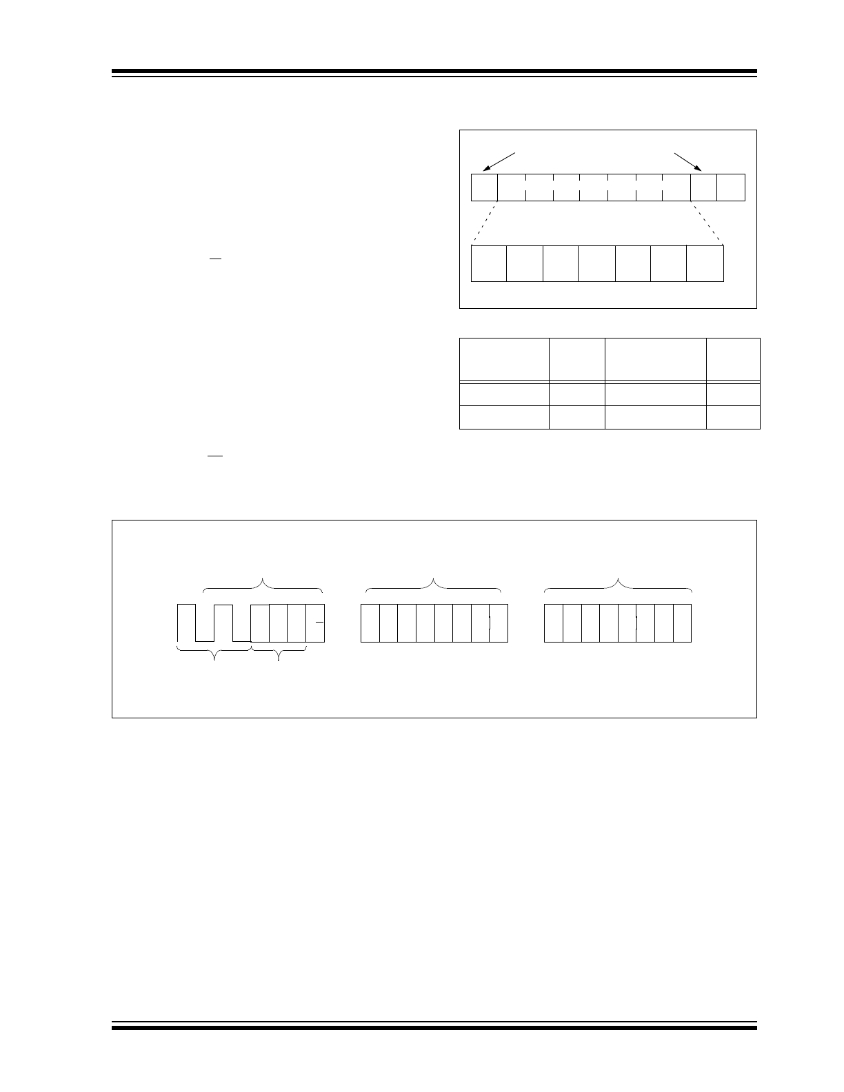
FIGURE 4-1:
BYTE WRITE
BUS ACTIVITY:
MASTER
SDA LINE
BUS ACTIVITY
CONTROL
BYTE
WORD
ADDRESS (1)
A
C
K
S
T
A
R
T
WORD
ADDRESS (0)
A
C
K
A
C
K
0
S
T
O
P
A
C
K
0 0 0
DATA
S
S
2004 Microchip Technology Inc.
DS21126E-page 7
24FC32
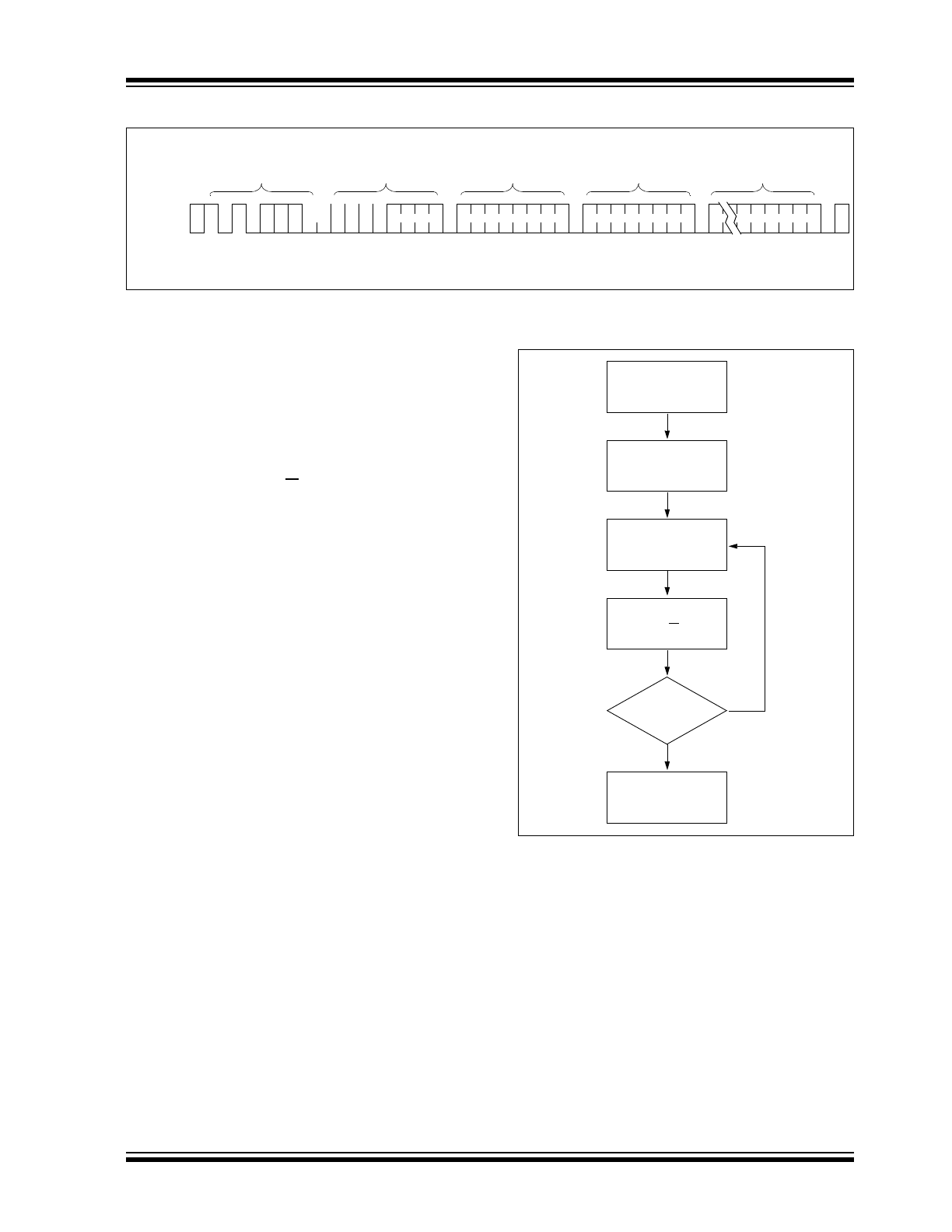
FIGURE 4-2:
PAGE WRITE
5.0
ACKNOWLEDGE POLLING
Since the device will not acknowledge during a write
cycle, this can be used to determine when the cycle is
complete (this feature can be used to maximize bus
throughput). Once the Stop condition for a Write
command has been issued from the master, the device
initiates the internally timed write cycle. ACK polling
can be initiated immediately. This involves the master
sending a Start condition followed by the control byte
for a Write command (R/W =
0
). If the device is still
busy with the write cycle, then no ACK will be returned.
If the cycle is complete, then the device will return the
ACK and the master can then proceed with the next
Read or Write command. See Figure 5-1 for flow
diagram.
FIGURE 5-1:
ACKNOWLEDGE
POLLING FLOW
BUS
MASTER
SDA LINE
BUS
CONTROL
BYTE
WORD
ADDRESS (1)
S
T
O
P
S
T
A
R
T
A
C
K
0
A
C
K
A
C
K
ACTIVITY
ACTIVITY
A
C
K
A
C
K
DATA n
DATA n+7
0 0 0
WORD
ADDRESS (0)
S
P
Did Device
Acknowledge
(ACK = 0)?
Send
Write Command
Send Stop
Condition to
Initiate Write Cycle
Send Start
Send Control Byte
with R/W =
0
Next
Operation
No
Yes

24FC32
DS21126E-page 8
2004 Microchip Technology Inc.
6.0
READ OPERATION
Read operations are initiated in the same way as write
operations with the exception that the R/W bit of the
slave address is set to one. There are three basic types
of read operations: current address read, random read,
and sequential read.
6.1
Current Address Read
The 24FC32 contains an address counter that
maintains the address of the last word accessed,
internally incremented by one. Therefore, if the
previous access (either a read or write operation) was
to address n (n is any legal address), the next current
address read operation would access data from
address n + 1. Upon receipt of the slave address with
R/W bit set to one, the 24FC32 issues an acknowledge
and transmits the eight bit data word. The master will
not acknowledge the transfer but does generate a Stop
condition and the 24FC32 discontinues transmission
(Figure 6-1).
6.2
Random Read
Random read operations allow the master to access
any memory location in a random manner. To perform
this type of read operation, first the word address must
be set. This is done by sending the word address to the
24FC32 as part of a write operation (R/W bit set to 0).
After the word address is sent, the master generates a
Start condition following the acknowledge. This
terminates the write operation, but not before the
internal address pointer is set. Then the master issues
the control byte again but with the R/W bit set to a one.
The 24FC32 will then issue an acknowledge and
transmit the eight bit data word. The master will not
acknowledge the transfer but does generate a Stop
condition which causes the 24FC32 to discontinue
transmission (Figure 6-2).
FIGURE 6-1:
CURRENT ADDRESS READ
6.3
Contiguous Addressing Across
Multiple Devices
The device select bits A2, A1, A0 can be used to
expand the contiguous address space for up to 256K
bits by adding up to eight 24FC32's on the same bus.
In this case, software can use A0 of the control byte as
address bit A12, A1 as address bit A13, and A2 as
address bit A14.
6.4
Sequential Read
Sequential reads are initiated in the same way as a
random read except that after the 24FC32 transmits
the first data byte, the master issues an acknowledge
as opposed to the Stop condition used in a random
read. This acknowledge directs the 24FC32 to transmit
the next sequentially addressed 8 bit word (Figure 6-3).
Following the final byte transmitted to the master, the
master will NOT generate an acknowledge but will
generate a Stop condition.
To provide sequential reads the 24FC32 contains an
internal address pointer which is incremented by one at
the completion of each operation. This address pointer
allows the entire memory contents to be serially read
during one operation. The address pointer, however,
will not roll over from address 07FF to address 0000. It
will roll from 07FF to unused memory space.
6.5
Noise Protection
The SCL and SDA inputs incorporate Schmitt Triggers
which suppress noise spikes to ensure proper device
operation even on a noisy bus.
CONTROL
A
C
K
S
T
A
R
T
S
T
O
P
BYTE
DATA n
BUS ACTIVITY
MASTER
SDA LINE
BUS ACTIVITY
A
C
K
N
O
S
P
2004 Microchip Technology Inc.
DS21126E-page 9
24FC32
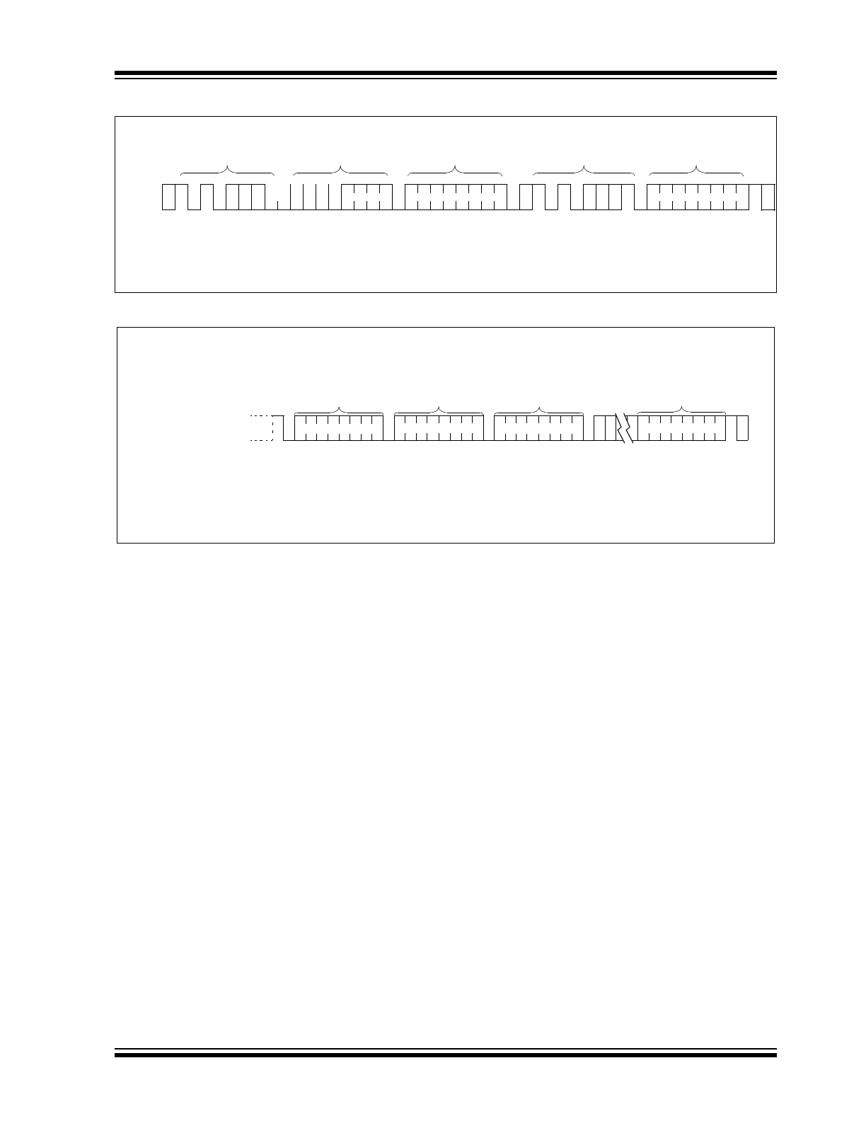
FIGURE 6-2:
RANDOM READ
FIGURE 6-3:
SEQUENTIAL READ
BUS
MASTER
SDA LINE
BUS
CONTROL
BYTE
WORD
ADDRESS (1)
S
T
O
P
S
T
A
R
T
A
C
K
A
C
K
A
C
K
ACTIVITY:
ACTIVITY:
A
C
K
N
O
DATA n
0 0 0 0
WORD
ADDRESS (0)
S
T
A
R
T
CONTROL
BYTE
A
C
K
P
S
S
P
BUS ACTIVITY
MASTER
SDA LINE
BUS ACTIVITY
S
T
O
P
CONTROL
BYTE
A
C
K
N
O
A
C
K
DATA n
DATA n + 1
DATA n + 2
DATA n + X
A
C
K
A
C
K
A
C
K

24FC32
DS21126E-page 10
2004 Microchip Technology Inc.
7.0
PAGE CACHE AND ARRAY
MAPPING
The cache is a 64 byte (8 pages x 8 bytes) FIFO buffer.
The cache allows the loading of up to 64 bytes of data
before the write cycle is actually begun, effectively
providing a 64-byte burst write at the maximum bus
rate. Whenever a Write command is initiated, the cache
starts loading and will continue to load until a Stop bit is
received to start the internal write cycle. The total
length of the write cycle will depend on how many
pages are loaded into the cache before the Stop bit is
given. Maximum cycle time for each page is 5 ms. Even
if a page is only partially loaded, it will still require the
same cycle time as a full page. If more than 64 bytes of
data are loaded before the Stop bit is given, the
address pointer will' wrap around' to the beginning of
cache page 0 and existing bytes in the cache will be
overwritten. The device will not respond to any
commands while the write cycle is in progress.
7.1
Cache Write Starting at a Page
Boundary
If a Write command begins at a page boundary
(address bits A2, A1 and A0 are zero), then all data
loaded into the cache will be written to the array in
sequential addresses. This includes writing across a
4K block boundary. In the example shown below,
(Figure 7-1) a Write command is initiated starting at
byte 0 of page 3 with a fully loaded cache (64 bytes).
The first byte in the cache is written to byte 0 of page 3
(of the array), with the remaining pages in the cache
written to sequential pages in the array. A write cycle is
executed after each page is written. Since the write
begins at page 3 and 8 pages are loaded into the
cache, the last 3 pages of the cache are written to the
next row in the array.
7.2
Cache Write Starting at a Non-
Page Boundary
When a Write command is initiated that does not begin
at a page boundary (i.e., address bits A2, A1 and A0
are not all zero), it is important to note how the data is
loaded into the cache, and how the data in the cache is
written to the array. When a Write command begins, the
first byte loaded into the cache is always loaded into
page 0. The byte within page 0 of the cache where the
load begins is determined by the three Least Significant
address bits (A2, A1, A0) that were sent as part of the
Write command. If the Write command does not start at
byte 0 of a page and the cache is fully loaded, then the
last byte(s) loaded into the cache will roll around to
page 0 of the cache and fill the remaining empty bytes.
If more than 64 bytes of data are loaded into the cache,
data already loaded will be overwritten.
In the example shown in Figure 7-2, a Write command
has been initiated starting at byte 2 of page 3 in the
array with a fully loaded cache of 64 bytes. Since the
cache started loading at byte 2, the last two bytes
loaded into the cache will 'roll over' and be loaded into
the first two bytes of page 0 (of the cache). When the
Stop bit is sent, page 0 of the cache is written to page
3 of the array. The remaining pages in the cache are
then loaded sequentially to the array. A write cycle is
executed after each page is written. If a partially loaded
page in the cache remains when the Stop bit is sent,
only the bytes that have been loaded will be written to
the array.
7.3
Power Management
This design incorporates a power Standby mode when
the device is not in use and automatically powers off
after the normal termination of any operation when a
Stop bit is received and all internal functions are
complete. This includes any error conditions (i.e., not
receiving an Acknowledge or Stop condition per the
two-wire bus specification). The device also
incorporates V
DD
monitor circuitry to prevent
inadvertent writes (data corruption) during low-voltage
conditions. The V
DD
monitor circuitry is powered off
when the device is in Standby mode in order to further
reduce power consumption.
2004 Microchip Technology Inc.
DS21126E-page 1
24FC32
Features
• Voltage operating range: 4.5V to 5.5V
- Maximum write current 3 mA at 5.5V
- Maximum read current 150
µ
A at 5.5V
- Standby current 1
µ
A typical
• 1 MHz SE2.bus two wire protocol
• Self-timed write cycle (including auto-erase)
• Power on/off data protection circuitry
• Endurance:
- 10,000,000 Erase/Write cycles ensured for a
4K block
- 1,000,000 E/W cycles ensured for a 28K
block
• 8-byte page, or byte modes available
• 1 page x 8 line input cache (64 bytes) for fast write
loads
• Schmitt Trigger inputs for noise suppression
• 2 ms typical write cycle time, byte or page
• Up to 8 chips may be connected to the same bus
for up to 256K bits total memory
• Electrostatic discharge protection > 4000V
• Data retention > 200 years
• 8-pin PDIP/SOIC packages
• Temperature ranges
Description
The Microchip Technology Inc. 24FC32 is a 4K x 8 (32K
bit) Serial Electrically Erasable PROM (EEPROM) with
a high-speed 1 MHz SE2.bus whose protocol is
functionally equivalent to the industry-standard I
2
C
bus. This device has been developed for advanced,
low power applications such as personal
communications or data acquisition. The 24FC32
features an input cache for fast write loads with a
capacity of eight 8-byte pages, or 64 bytes. It also
features a fixed 4K-bit block of ultra-high endurance
memory for data that changes frequently. The 24FC32
is capable of both random and sequential reads up to
the 32K boundary. Functional address lines allow up to
eight 24FC32 devices on the same bus, for up to 256K
bits address space. The 24FC32 is available in the
standard 8-pin plastic DIP and 8-pin surface mount
SOIC package.
Package Types
Block Diagram
Pin Function Table
- Commercial (C):
0°C
to
+70°C
- Industrial (I):
-40°C
to
+85°C
Name
Function
A0, A1, A2
User Configurable Chip Selects
V
SS
Ground
SDA
Serial Address/Data I/O
SCL
Serial Clock
V
CC
+4.5V to 5.5V Power Supply
NC
No Internal Connection
24F
C
3
2
SOIC
1
2
3
4
8
7
6
5
Vcc
NC
SCL
SDA
A0
A1
A2
Vss
24F
C
3
2
PDIP
1
2
3
4
8
7
6
5
Vcc
NC
SCL
SDA
A0
A1
A2
Vss
HV Generator
EEPROM
Array
Page Latches
YDEC
XDEC
Sense AMP
R/W Control
Memory
Control
Logic
I/O
Control
Logic
SDA
SCL
V
CC
V
SS
I/O
A2
A1
A0
Cache
32K 5.0V 1 MHz I
2
C
™
Smart Serial
™
EEPROM
I
2
C is a trademark of Philips Corporation.
Smart Serial is a trademark of Microchip Technology Inc.
Obsolete Device
Please use 24LC32A or 24LC65.
24FC32
DS21126E-page 2
2004 Microchip Technology Inc.
1.0
ELECTRICAL CHARACTERISTICS
Absolute Maximum Ratings
(†)
V
CC
.............................................................................................................................................................................7.0V
All inputs and outputs w.r.t. V
SS
......................................................................................................... -0.6V to V
CC
+1.0V
Storage temperature ...............................................................................................................................-65°C to +150°C
Ambient temperature with power applied ................................................................................................-65°C to +125°C
ESD protection on all pins
......................................................................................................................................................≥
4 kV
TABLE 1:
DC CHARACTERISTICS
FIGURE 1-1:
BUS TIMING START/STOP
† NOTICE: Stresses above those listed under “Absolute Maximum Ratings” may cause permanent damage to
the device. This is a stress rating only and functional operation of the device at those or any other conditions
above those indicated in the operational listings of this specification is not implied. Exposure to maximum rating
conditions for extended periods may affect device reliability.
DC CHARACTERISTICS
V
CC
= +4.5V to +5.5V
Commercial (C): T
A
= 0°C to +70°C
Industrial (I):
T
A
= -40°C to +85°C
Parameter
Symbol
Min
Max
Units
Conditions
A0, A1, A2, SCL and SDA pins:
High-level input voltage
V
IH
0.7 Vcc
—
V
Low-level input voltage
V
IL
—
0.3 Vcc
V
Hysteresis of SCL and SDA
V
HYS
0.05 Vcc
—
V
(Note)
Low-level output voltage of SDA
V
OL
—
0.40
V
I
OL
= 3.0 mA
Input leakage current
I
LI
—
±1
µ
A
Vin = 0.1V to Vcc
Output leakage current
I
LO
—
±1
µ
A
V
OUT
= 0.1V to V
CC
Pin capacitance
(all inputs/outputs)
C
INT
—
10
pF
V
CC
= 5.0V (Note)
T
A
= 25°C, F
CLK
= 1 MHz
Operating current
Icc Write
I
CC
Read
—
—
3
150
mA
µ
A
V
CC
= 5.5V, SCL = 1 MHz
V
CC
= 5.5V, SCL = 1 MHz
Standby current
I
CCS
—
5
(1 typical)
µ
A
V
CC
= 5.5V,
SCL = SDA = V
CC
A0, A1, A2 = V
SS
Note:
This parameter is periodically sampled and not 100% tested.
T
SU
:
STA
T
HD
:
STA
V
HYS
T
SU
:
STO
START
STOP
SCL
SDA
2004 Microchip Technology Inc.
DS21126E-page 3
24FC32
TABLE 1-1:
AC CHARACTERISTICS
FIGURE 1-2:
BUS TIMING DATA
Parameter
Symbol
1 MHz Bus
Units
Remarks
Min
Max
Clock frequency
F
CLK
0
1000
kHz
Clock high time
T
HIGH
500
—
ns
Clock low time
T
LOW
500
—
ns
SDA and SCL rise time
T
R
—
300
ns
(Note 1)
SDA and SCL fall time
T
F
—
100
ns
(Note 1)
Start condition hold time
T
HD
:
STA
250
—
ns
After this period the first clock pulse is
generated
Start condition setup time
T
SU
:
STA
250
—
ns
Only relevant for repeated Start condition
Data input hold time
T
HD
:
DAT
0
—
ns
Data input setup time
T
SU
:
DAT
100
—
ns
Stop condition setup time
T
SU
:
STO
250
—
ns
Output valid from clock
T
AA
—
350
ns
(Note 2)
Bus free time
T
BUF
500
—
ns
Time the bus must be free before a new
transmission can start
Write cycle time
T
WR
—
5
ms/page Note 3
Endurance
High Endurance
Block
Rest of Array
—
—
10M
1M
—
—
10M
1M
25°C, Vcc = 5.0V, Block mode (Note 4)
Note 1:
Not 100 percent tested.
2:
As a transmitter, the device must provide an internal minimum delay time to bridge the undefined region
(minimum 100 ns) of the falling edge of SCL to avoid unintended generation of Start or Stop conditions.
3:
The times shown are for a single page of 8 bytes. Multiply by the number of pages loaded into the write
cache for total time.
4:
This parameter is not tested but ensured by characterization. For endurance estimates in a specific
application, please consult the Total Endurance™ Model which can be obtained from our web site.
SCL
SDA
IN
SDA
OUT
T
SU
:
STA
T
SP
T
AA
T
F
T
LOW
T
HIGH
T
HD
:
STA
T
HD
:
DAT
T
SU
:
DAT
T
SU
:
STO
T
BUF
T
AA
T
R
24FC32
DS21126E-page 4
2004 Microchip Technology Inc.
2.0
FUNCTIONAL DESCRIPTION
The 24FC32 supports a bidirectional two-wire bus and
data transmission protocol. A device that sends data
onto the bus is defined as transmitter, and a device
receiving data as receiver. The bus must be controlled
by a master device which generates the serial clock
(SCL), controls the bus access, and generates the Start
and Stop conditions, while the 24FC32 works as slave.
Both master and slave can operate as transmitter or
receiver but the master device determines which mode
is activated.
3.0
BUS CHARACTERISTICS
The following bus protocol has been defined:
• Data transfer may be initiated only when the bus
is not busy.
• During data transfer, the data line must remain
stable whenever the clock line is high. Changes in
the data line while the clock line is high will be
interpreted as a Start or Stop condition.
Accordingly, the following bus conditions have been
defined (Figure 3-1).
3.1
Bus not Busy (A)
Both data and clock lines remain high.
3.2
Start Data Transfer (B)
A high-to-low transition of the SDA line while the clock
(SCL) is high determines a Start condition. All
commands must be preceded by a Start condition.
3.3
Stop Data Transfer (C)
A low-to-high transition of the SDA line while the clock
(SCL) is high determines a Stop condition. All
operations must be ended with a Stop condition.
3.4
Data Valid (D)
The state of the data line represents valid data when,
after a Start condition, the data line is stable for the
duration of the high period of the clock signal.
The data on the line must be changed during the low
period of the clock signal. There is one clock pulse per
bit of data.
Each data transfer is initiated with a Start condition and
terminated with a Stop condition. The number of the
data bytes transferred between the Start and Stop
conditions is determined by the master device.
3.5
Acknowledge
Each receiving device, when addressed, is obliged to
generate an Acknowledge signal after the reception of
each byte. The master device must generate an extra
clock pulse which is associated with this Acknowledge
bit.
A device that acknowledges must pull down the SDA
line during the Acknowledge clock pulse in such a way
that the SDA line is stable low during the high period of
the acknowledge related clock pulse. Of course, setup
and hold times must be taken into account. During
reads, a master must signal an end of data to the slave
by NOT generating an Acknowledge bit on the last byte
that has been clocked out of the slave. In this case, the
slave (24FC32) will leave the data line high to enable
the master to generate the Stop condition.
FIGURE 3-1:
DATA TRANSFER SEQUENCE ON THE SERIAL BUS
Note:
The 24FC32 does not generate any
Acknowledge bits if an internal
programming cycle is in progress.
SCL
SDA
(A)
(B)
(D)
(D)
(C)
(A)
START CONDITION
ADDRESS
OR
ACKNOWLEDGE
VALID
DATA ALLOWED
TO CHANGE
STOP
CONDITION
2004 Microchip Technology Inc.
DS21126E-page 5
24FC32
3.6
Device Addressing
A control byte is the first byte received following the
Start condition from the master device. The control byte
consists of a four bit control code; for the 24FC32 this
is set as ‘
1010
’ binary for read and write operations.
The next three bits of the control byte are the device
select bits (A2, A1, A0). They are used by the master
device to select which of the eight devices are to be
accessed. These bits are in effect the three Most
Significant bits of the word address. The last bit of the
control byte (R/W) defines the operation to be
performed. When set to a one a read operation is
selected, and when set to a zero a write operation is
selected. The next two bytes received define the
address of the first data byte (Figure 3-3). Because
only A11..A0 are used, the upper four address bits must
be zeros. The Most Significant bit of the Most
Significant Byte of the address is transferred first.
Following the Start condition, the 24FC32 monitors the
SDA bus checking the device type identifier being
transmitted. Upon receiving a ‘
1010
’ code and
appropriate device select bits, the slave device outputs
an Acknowledge signal on the SDA line. Depending on
the state of the R/W bit, the 24FC32 will select a read
or write operation.
FIGURE 3-2:
CONTROL BYTE
ALLOCATION
FIGURE 3-3:
ADDRESS SEQUENCE BIT ASSIGNMENTS
Operation
Control
Code
Device Select
R/W
Read
1010
Device Address
1
Write
1010
Device Address
0
SLAVE ADDRESS
X = Don’t care
1
0
1
0
A2
A1
A0
R/W
A
START
READ/WRITE
CONTROL
BYTE
ADDRESS
BYTE 1
1
0
1
0
0
0
0
0
A
2
A
0
A
1
R
/
W
Slave
Address
Device
Select
Bits
A
11
A
10
A
9
A
8
A
7
• •
• • •
A
0
•
ADDRESS
BYTE 0
24FC32
DS21126E-page 6
2004 Microchip Technology Inc.
4.0
WRITE OPERATION
4.1
Split Endurance
The 24FC32 is organized as a continuous 32K block of
memory. However, the first 4K, starting at address 000,
is rated at 10,000,000 E/W cycles ensured. The
remainder of the array, 28K bits, is rated at 100K E/W
cycles ensured. This feature is helpful in applications in
which some data change frequently, while a majority of
the data change infrequently. One example would be a
cellular telephone in which last-number redial and
microcontroller scratch pad require a high-endurance
block, while speed dials and lookup tables change
infrequently and so require only a standard endurance
rating.
4.2
Byte Write
Following the Start condition from the master, the
control code (four bits), the device select (three bits),
and the R/W bit which is a logic low are clocked onto
the bus by the master transmitter. This indicates to the
addressed slave receiver that a byte with a word
address will follow after it has generated an
Acknowledge bit during the ninth clock cycle. Therefore
the next byte transmitted by the master is the high-
order byte of the word address and will be written into
the address pointer of the 24FC32. The next byte is the
Least Significant Address Byte. After receiving another
Acknowledge signal from the 24FC32 the master
device will transmit the data word to be written into the
addressed memory location. The 24FC32
acknowledges again and the master generates a Stop
condition. This initiates the internal write cycle, and
during this time the 24FC32 will not generate
Acknowledge signals (Figure 4-1).
4.3
Page Write
The write control byte, word address and the first data
byte are transmitted to the 24FC32 in the same way as
in a byte write. But instead of generating a Stop
condition, the master transmits up to eight pages of
eight data bytes each (64 bytes total) which are
temporarily stored in the on-chip page cache of the
24FC32. They will be written from cache into the
EEPROM array after the master has transmitted a Stop
condition. After the receipt of each word, the six lower
order address pointer bits are internally incremented by
one. The higher order seven bits of the word address
remain constant. If the master should transmit more
than eight bytes prior to generating the Stop condition
(writing across a page boundary), the address counter
(lower three bits) will roll over and the pointer will be
incremented to point to the next line in the cache. This
can continue to occur up to eight times or until the
cache is full, at which time a Stop condition should be
generated by the master. If a Stop condition is not
received, the cache pointer will roll over to the first line
(byte 0) of the cache, and any further data received will
overwrite previously captured data. The Stop condition
can be sent at any time during the transfer. As with the
byte write operation, once a Stop condition is received,
an internal write cycle will begin. The 64-byte cache will
continue to capture data until a Stop condition occurs or
the operation is aborted (Figure 4-2).
FIGURE 4-1:
BYTE WRITE
BUS ACTIVITY:
MASTER
SDA LINE
BUS ACTIVITY
CONTROL
BYTE
WORD
ADDRESS (1)
A
C
K
S
T
A
R
T
WORD
ADDRESS (0)
A
C
K
A
C
K
0
S
T
O
P
A
C
K
0 0 0
DATA
S
S
2004 Microchip Technology Inc.
DS21126E-page 7
24FC32
FIGURE 4-2:
PAGE WRITE
5.0
ACKNOWLEDGE POLLING
Since the device will not acknowledge during a write
cycle, this can be used to determine when the cycle is
complete (this feature can be used to maximize bus
throughput). Once the Stop condition for a Write
command has been issued from the master, the device
initiates the internally timed write cycle. ACK polling
can be initiated immediately. This involves the master
sending a Start condition followed by the control byte
for a Write command (R/W =
0
). If the device is still
busy with the write cycle, then no ACK will be returned.
If the cycle is complete, then the device will return the
ACK and the master can then proceed with the next
Read or Write command. See Figure 5-1 for flow
diagram.
FIGURE 5-1:
ACKNOWLEDGE
POLLING FLOW
BUS
MASTER
SDA LINE
BUS
CONTROL
BYTE
WORD
ADDRESS (1)
S
T
O
P
S
T
A
R
T
A
C
K
0
A
C
K
A
C
K
ACTIVITY
ACTIVITY
A
C
K
A
C
K
DATA n
DATA n+7
0 0 0
WORD
ADDRESS (0)
S
P
Did Device
Acknowledge
(ACK = 0)?
Send
Write Command
Send Stop
Condition to
Initiate Write Cycle
Send Start
Send Control Byte
with R/W =
0
Next
Operation
No
Yes
24FC32
DS21126E-page 8
2004 Microchip Technology Inc.
6.0
READ OPERATION
Read operations are initiated in the same way as write
operations with the exception that the R/W bit of the
slave address is set to one. There are three basic types
of read operations: current address read, random read,
and sequential read.
6.1
Current Address Read
The 24FC32 contains an address counter that
maintains the address of the last word accessed,
internally incremented by one. Therefore, if the
previous access (either a read or write operation) was
to address n (n is any legal address), the next current
address read operation would access data from
address n + 1. Upon receipt of the slave address with
R/W bit set to one, the 24FC32 issues an acknowledge
and transmits the eight bit data word. The master will
not acknowledge the transfer but does generate a Stop
condition and the 24FC32 discontinues transmission
(Figure 6-1).
6.2
Random Read
Random read operations allow the master to access
any memory location in a random manner. To perform
this type of read operation, first the word address must
be set. This is done by sending the word address to the
24FC32 as part of a write operation (R/W bit set to 0).
After the word address is sent, the master generates a
Start condition following the acknowledge. This
terminates the write operation, but not before the
internal address pointer is set. Then the master issues
the control byte again but with the R/W bit set to a one.
The 24FC32 will then issue an acknowledge and
transmit the eight bit data word. The master will not
acknowledge the transfer but does generate a Stop
condition which causes the 24FC32 to discontinue
transmission (Figure 6-2).
FIGURE 6-1:
CURRENT ADDRESS READ
6.3
Contiguous Addressing Across
Multiple Devices
The device select bits A2, A1, A0 can be used to
expand the contiguous address space for up to 256K
bits by adding up to eight 24FC32's on the same bus.
In this case, software can use A0 of the control byte as
address bit A12, A1 as address bit A13, and A2 as
address bit A14.
6.4
Sequential Read
Sequential reads are initiated in the same way as a
random read except that after the 24FC32 transmits
the first data byte, the master issues an acknowledge
as opposed to the Stop condition used in a random
read. This acknowledge directs the 24FC32 to transmit
the next sequentially addressed 8 bit word (Figure 6-3).
Following the final byte transmitted to the master, the
master will NOT generate an acknowledge but will
generate a Stop condition.
To provide sequential reads the 24FC32 contains an
internal address pointer which is incremented by one at
the completion of each operation. This address pointer
allows the entire memory contents to be serially read
during one operation. The address pointer, however,
will not roll over from address 07FF to address 0000. It
will roll from 07FF to unused memory space.
6.5
Noise Protection
The SCL and SDA inputs incorporate Schmitt Triggers
which suppress noise spikes to ensure proper device
operation even on a noisy bus.
CONTROL
A
C
K
S
T
A
R
T
S
T
O
P
BYTE
DATA n
BUS ACTIVITY
MASTER
SDA LINE
BUS ACTIVITY
A
C
K
N
O
S
P
2004 Microchip Technology Inc.
DS21126E-page 9
24FC32
FIGURE 6-2:
RANDOM READ
FIGURE 6-3:
SEQUENTIAL READ
BUS
MASTER
SDA LINE
BUS
CONTROL
BYTE
WORD
ADDRESS (1)
S
T
O
P
S
T
A
R
T
A
C
K
A
C
K
A
C
K
ACTIVITY:
ACTIVITY:
A
C
K
N
O
DATA n
0 0 0 0
WORD
ADDRESS (0)
S
T
A
R
T
CONTROL
BYTE
A
C
K
P
S
S
P
BUS ACTIVITY
MASTER
SDA LINE
BUS ACTIVITY
S
T
O
P
CONTROL
BYTE
A
C
K
N
O
A
C
K
DATA n
DATA n + 1
DATA n + 2
DATA n + X
A
C
K
A
C
K
A
C
K
24FC32
DS21126E-page 10
2004 Microchip Technology Inc.
7.0
PAGE CACHE AND ARRAY
MAPPING
The cache is a 64 byte (8 pages x 8 bytes) FIFO buffer.
The cache allows the loading of up to 64 bytes of data
before the write cycle is actually begun, effectively
providing a 64-byte burst write at the maximum bus
rate. Whenever a Write command is initiated, the cache
starts loading and will continue to load until a Stop bit is
received to start the internal write cycle. The total
length of the write cycle will depend on how many
pages are loaded into the cache before the Stop bit is
given. Maximum cycle time for each page is 5 ms. Even
if a page is only partially loaded, it will still require the
same cycle time as a full page. If more than 64 bytes of
data are loaded before the Stop bit is given, the
address pointer will' wrap around' to the beginning of
cache page 0 and existing bytes in the cache will be
overwritten. The device will not respond to any
commands while the write cycle is in progress.
7.1
Cache Write Starting at a Page
Boundary
If a Write command begins at a page boundary
(address bits A2, A1 and A0 are zero), then all data
loaded into the cache will be written to the array in
sequential addresses. This includes writing across a
4K block boundary. In the example shown below,
(Figure 7-1) a Write command is initiated starting at
byte 0 of page 3 with a fully loaded cache (64 bytes).
The first byte in the cache is written to byte 0 of page 3
(of the array), with the remaining pages in the cache
written to sequential pages in the array. A write cycle is
executed after each page is written. Since the write
begins at page 3 and 8 pages are loaded into the
cache, the last 3 pages of the cache are written to the
next row in the array.
7.2
Cache Write Starting at a Non-
Page Boundary
When a Write command is initiated that does not begin
at a page boundary (i.e., address bits A2, A1 and A0
are not all zero), it is important to note how the data is
loaded into the cache, and how the data in the cache is
written to the array. When a Write command begins, the
first byte loaded into the cache is always loaded into
page 0. The byte within page 0 of the cache where the
load begins is determined by the three Least Significant
address bits (A2, A1, A0) that were sent as part of the
Write command. If the Write command does not start at
byte 0 of a page and the cache is fully loaded, then the
last byte(s) loaded into the cache will roll around to
page 0 of the cache and fill the remaining empty bytes.
If more than 64 bytes of data are loaded into the cache,
data already loaded will be overwritten.
In the example shown in Figure 7-2, a Write command
has been initiated starting at byte 2 of page 3 in the
array with a fully loaded cache of 64 bytes. Since the
cache started loading at byte 2, the last two bytes
loaded into the cache will 'roll over' and be loaded into
the first two bytes of page 0 (of the cache). When the
Stop bit is sent, page 0 of the cache is written to page
3 of the array. The remaining pages in the cache are
then loaded sequentially to the array. A write cycle is
executed after each page is written. If a partially loaded
page in the cache remains when the Stop bit is sent,
only the bytes that have been loaded will be written to
the array.
7.3
Power Management
This design incorporates a power Standby mode when
the device is not in use and automatically powers off
after the normal termination of any operation when a
Stop bit is received and all internal functions are
complete. This includes any error conditions (i.e., not
receiving an Acknowledge or Stop condition per the
two-wire bus specification). The device also
incorporates V
DD
monitor circuitry to prevent
inadvertent writes (data corruption) during low-voltage
conditions. The V
DD
monitor circuitry is powered off
when the device is in Standby mode in order to further
reduce power consumption.