
2003-2012 Microchip Technology Inc.
DS21117B-page 1
MCP6S21/2/6/8
Features
• Multiplexed Inputs: 1, 2, 6 or 8 channels
• 8 Gain Selections:
- +1, +2, +4, +5, +8, +10, +16 or +32 V/V
• Serial Peripheral Interface (SPI)
• Rail-to-Rail Input and Output
• Low Gain Error: ±1% (max)
• Low Offset: ±275 µV (max)
• High Bandwidth: 2 to 12 MHz (typ)
• Low Noise: 10 nV/
Hz @ 10 kHz (typ)
• Low Supply Current: 1.0 mA (typ)
• Single Supply: 2.5V to 5.5V
Typical Applications
• A/D Converter Driver
• Multiplexed Analog Applications
• Data Acquisition
• Industrial Instrumentation
• Test Equipment
• Medical Instrumentation
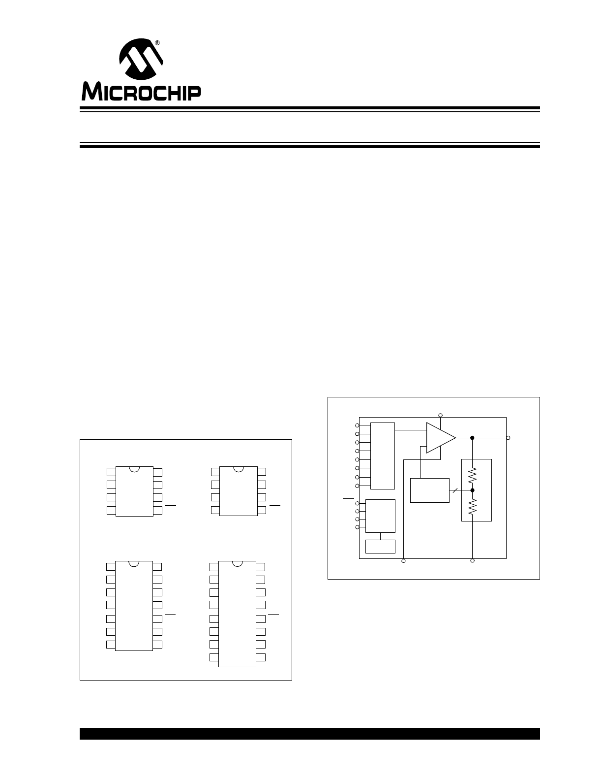
Package Types
Description
The Microchip Technology Inc. MCP6S21/2/6/8 are
analog Programmable Gain Amplifiers (PGA). They
can be configured for gains from +1 V/V to +32 V/V and
the input multiplexer can select one of up to eight chan-
nels through an SPI port. The serial interface can also
put the PGA into shutdown to conserve power. These
PGAs are optimized for high speed, low offset voltage
and single-supply operation with rail-to-rail input and
output capability. These specifications support single
supply applications needing flexible performance or
multiple inputs.
The one channel MCP6S21 and the two channel
MCP6S22 are available in 8-pin PDIP, SOIC and
MSOP packages. The six channel MCP6S26 is avail-
able in 14-pin PDIP, SOIC and TSSOP packages. The
eight channel MCP6S28 is available in 16-pin PDIP
and SOIC packages. All parts are fully specified from
-40°C to +85°C.
Block Diagram
V
REF
CH0
V
SS
SI
SCK
1
2
3
4
8
7
6
5
V
DD
CS
V
OUT
CH1
CH0
CH2
CS
SI
1
2
3
4
14
13
12
11
V
REF
V
SS
V
OUT
5
6
7
10
9
8
CH3
SCK
V
DD
CH5
CH4
CH0
V
OUT
CH1
V
SS
CS
1
2
3
4
16
15
14
13 SI
SCK
5
6
7
12
11
10
CH2
CH4
CH7
V
DD
CH5
8
9
SO
CH6
CH3
SO
CH1
CH0
V
SS
SI
SCK
1
2
3
4
8
7
6
5
V
DD
CS
V
OUT
MCP6S21
PDIP, SOIC, MSOP
MCP6S26
PDIP, SOIC, TSSOP
MCP6S28
PDIP, SOIC
MCP6S22
PDIP, SOIC, MSOP
V
REF
V
OUT
V
REF
V
DD
CS
SI
SO
SCK
CH1
CH0
CH3
CH2
CH5
CH4
CH7
CH6
V
SS
8
R
F
R
G
MUX
SPI™
Logic
POR
Gain
Switches
+
-
R
e
sist
or Ladd
er (R
LA
D
)
Single-Ended, Rail-to-Rail I/O, Low Gain PGA
MCP6S21/2/6/8
DS21117B-page 2
2003-2012 Microchip Technology Inc.
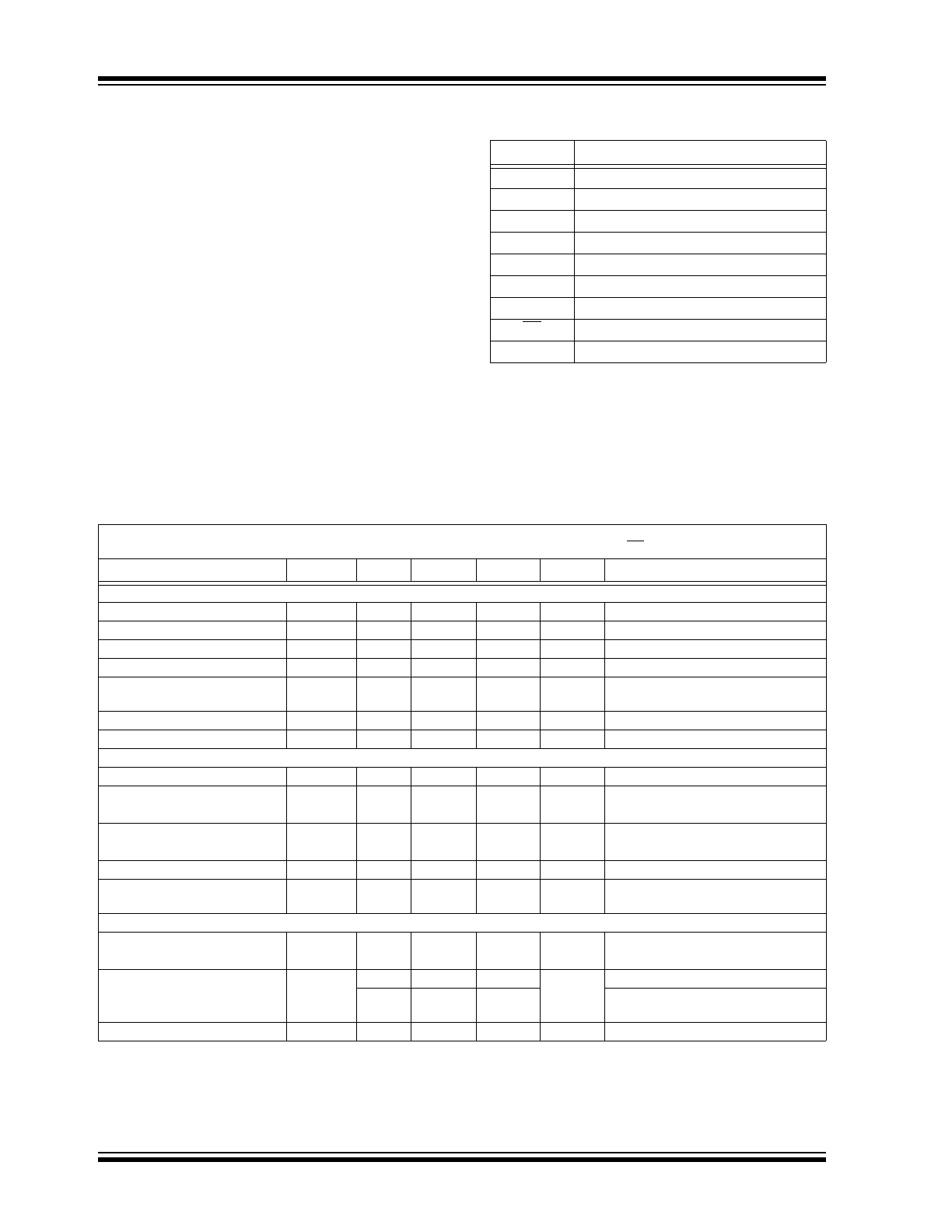
1.0
ELECTRICAL
CHARACTERISTICS
Absolute Maximum Ratings †
V
DD
- V
SS
.........................................................................7.0V
All inputs and outputs ....................... V
SS
- 0.3V to V
DD
+0.3V
Difference Input voltage ........................................ |V
DD
- V
SS
|
Output Short Circuit Current...................................continuous
Current at Input Pin
2 mA
Current at Output and Supply Pins
30 mA
Storage temperature .....................................-65°C to +150°C
Junction temperature .................................................. +150°C
ESD protection on all pins (HBM;MM)
2 kV; 200V
† Notice: Stresses above those listed under "Maximum
Ratings" may cause permanent damage to the device. This is
a stress rating only and functional operation of the device at
those or any other conditions above those indicated in the
operation listings of this specification is not implied. Exposure
to maximum rating conditions for extended periods may affect
device reliability.
PIN FUNCTION TABLE
Name
Function
V
OUT
Analog Output
CH0-CH7
Analog Inputs
V
SS
Negative Power Supply
V
DD
Positive Power Supply
SCK
SPI Clock Input
SI
SPI Serial Data Input
SO
SPI Serial Data Output
CS
SPI Chip Select
V
REF
External Reference Pin
DC CHARACTERISTICS
Electrical Specifications: Unless otherwise indicated, T
A
= +25°C, V
DD
= +2.5V to +5.5V, V
SS
= GND, V
REF
= V
SS
, G = +1 V/V,
Input = CH0 = (0.3V)/G, CH1 to CH7 = 0.3V, R
L
= 10 k
to V
DD
/2, SI and SCK are tied low and CS is tied high.
Parameters
Sym
Min
Typ
Max
Units
Conditions
Amplifier Input
Input Offset Voltage
V
OS
-275
—
+275
µV
G = +1, V
DD
= 4.0V
Input Offset Voltage Drift
V
OS
/
T
A
—
±4
—
µV/°C
T
A
= -40 to +85°C
Power Supply Rejection Ratio
PSRR
70
85
—
dB
G = +1 (Note 1)
Input Bias Current
I
B
—
±1
—
pA
CHx = V
DD
/2
Input Bias Current over
Temperature
I
B
—
—
250
pA
T
A
= -40 to +85°C,
CHx = V
DD
/2
Input Impedance
Z
IN
—
10
13
||15
—
||pF
Input Voltage Range
V
IVR
V
SS
0.3
—
V
DD
+0.3
V
Amplifier Gain
Nominal Gains
—
—
1 to 32
—
V/V
+1, +2, +4, +5, +8, +10, +16 or +32
DC Gain Error
G = +1
g
E
-0.1
—
+0.1
%
V
OUT
0.3V to V
DD
0.3V
G
+2
g
E
-1.0
—
+1.0
%
V
OUT
0.3V to V
DD
0.3V
DC Gain Drift
G = +1
G/T
A
—
±0.0002
—
%/°C
T
A
= -40 to +85°C
G
+2
G/T
A
—
±0.0004
—
%/°C
T
A
= -40 to +85°C
Internal Resistance
R
LAD
3.4
4.9
6.4
k
(Note 1)
Internal Resistance over
Temperature
R
LAD
/
T
A
—
+0.028
—
%/°C
(Note 1)
T
A
= -40 to +85°C
Amplifier Output
DC Output Non-linearity G = +1
V
ONL
—
±0.003
—
% of FSR V
OUT
= 0.3V to V
DD
0.3V, V
DD
= 5.0V
G
+2
V
ONL
—
±0.001
—
% of FSR V
OUT
= 0.3V to V
DD
0.3V, V
DD
= 5.0V
Maximum Output Voltage Swing
V
OH
, V
OL
V
SS
+20
—
V
DD
-100
mV
G
+2; 0.5V output overdrive
V
SS
+60
—
V
DD
-60
G
+2; 0.5V output overdrive,
V
REF
= V
DD
/2
Short-Circuit Current
I
O(SC)
—
±30
—
mA
Note
1: R
LAD
(R
F
+ R
G
in Figure 4-1) connects V
REF
, V
OUT
and the inverting input of the internal amplifier. The MCP6S22 has
V
REF
tied internally to V
SS
, so V
SS
is coupled to the internal amplifier and the PSRR spec describes PSRR+ only. We
recommend the MCP6S22’s V
SS
pin be tied directly to ground to avoid noise problems.
2: I
Q
includes current in R
LAD
(typically 60 µA at V
OUT
= 0.3V). Both I
Q
and I
Q_SHDN
exclude digital switching currents.
3: The output goes Hi-Z and the registers reset to their defaults; see Section 5.4, “Power-On Reset”.
2003-2012 Microchip Technology Inc.
DS21117B-page 3
MCP6S21/2/6/8
Power Supply
Supply Voltage
V
DD
2.5
—
5.5
V
Quiescent Current
I
Q
0.5
1.0
1.35
mA
I
O
= 0 (Note 2)
Quiescent Current, Shutdown
mode
I
Q_SHDN
—
0.5
1.0
µA
I
O
= 0 (Note 2)
Power-On Reset
POR Trip Voltage
V
POR
1.2
1.7
2.2
V
(Note 3)
POR Trip Voltage Drift
V
POR
/
T
—
-3.0
—
mV/°C
T
A
= -40°C to+85°C
DC CHARACTERISTICS (CONTINUED)
Electrical Specifications: Unless otherwise indicated, T
A
= +25°C, V
DD
= +2.5V to +5.5V, V
SS
= GND, V
REF
= V
SS
, G = +1 V/V,
Input = CH0 = (0.3V)/G, CH1 to CH7 = 0.3V, R
L
= 10 k
to V
DD
/2, SI and SCK are tied low and CS is tied high.
Parameters
Sym
Min
Typ
Max
Units
Conditions
Note
1: R
LAD
(R
F
+ R
G
in Figure 4-1) connects V
REF
, V
OUT
and the inverting input of the internal amplifier. The MCP6S22 has
V
REF
tied internally to V
SS
, so V
SS
is coupled to the internal amplifier and the PSRR spec describes PSRR+ only. We
recommend the MCP6S22’s V
SS
pin be tied directly to ground to avoid noise problems.
2: I
Q
includes current in R
LAD
(typically 60 µA at V
OUT
= 0.3V). Both I
Q
and I
Q_SHDN
exclude digital switching currents.
3: The output goes Hi-Z and the registers reset to their defaults; see Section 5.4, “Power-On Reset”.
AC CHARACTERISTICS
Electrical Specifications: Unless otherwise indicated, T
A
= +25°C, V
DD
= +2.5V to +5.5V, V
SS
= GND, V
REF
= V
SS
, G = +1 V/V,
Input = CH0 =(0.3V)/G, CH1 to CH7=0.3V, R
L
= 10 k
to V
DD
/2, C
L
= 60 pF, SI and SCK are tied low, and CS is tied high.
Parameters
Sym
Min
Typ
Max
Units
Conditions
Frequency Response
-3 dB Bandwidth
BW
—
2 to 12
—
MHz
All gains; V
OUT
< 100 mV
P-P
(Note 1)
Gain Peaking
GPK
—
0
—
dB
All gains; V
OUT
< 100 mV
P-P
Total Harmonic Distortion plus Noise
f = 1 kHz, G = +1 V/V
THD+N
—
0.0015
—
%
V
OUT
= 1.5V ± 1.0V
PK
, V
DD
= 5.0V,
BW = 22 kHz
f = 1 kHz, G = +4 V/V
THD+N
—
0.0058
—
%
V
OUT
= 1.5V ± 1.0V
PK
, V
DD
= 5.0V,
BW = 22 kHz
f = 1 kHz, G = +16 V/V
THD+N
—
0.023
—
%
V
OUT
= 1.5V ± 1.0V
PK
, V
DD
= 5.0V,
BW = 22 kHz
f = 20 kHz, G = +1 V/V
THD+N
—
0.0035
—
%
V
OUT
= 1.5V ± 1.0V
PK
, V
DD
= 5.0V,
BW = 80 kHz
f = 20 kHz, G = +4 V/V
THD+N
—
0.0093
—
%
V
OUT
= 1.5V ± 1.0V
PK
, V
DD
= 5.0V,
BW = 80 kHz
f = 20 kHz, G = +16 V/V
THD+N
—
0.036
—
%
V
OUT
= 1.5V ± 1.0V
PK
, V
DD
= 5.0V,
BW = 80 kHz
Step Response
Slew Rate
SR
—
4.0
—
V/µs
G = 1, 2
—
11
—
V/µs
G = 4, 5, 8, 10
—
22
—
V/µs
G = 16, 32
Noise
Input Noise Voltage
E
ni
—
3.2
—
µV
P-P
f = 0.1 Hz to 10 kHz (Note 2)
—
26
—
f = 0.1 Hz to 200 kHz (Note 2)
Input Noise Voltage Density
e
ni
—
10
—
nV/
Hz f = 10 kHz (Note 2)
Input Noise Current Density
i
ni
—
4
—
fA/
Hz f = 10 kHz
Note
1: See Table 4-1 for a list of typical numbers.
2: E
ni
and e
ni
include ladder resistance noise. See Figure 2-33 for e
ni
vs. G data.
MCP6S21/2/6/8
DS21117B-page 4
2003-2012 Microchip Technology Inc.
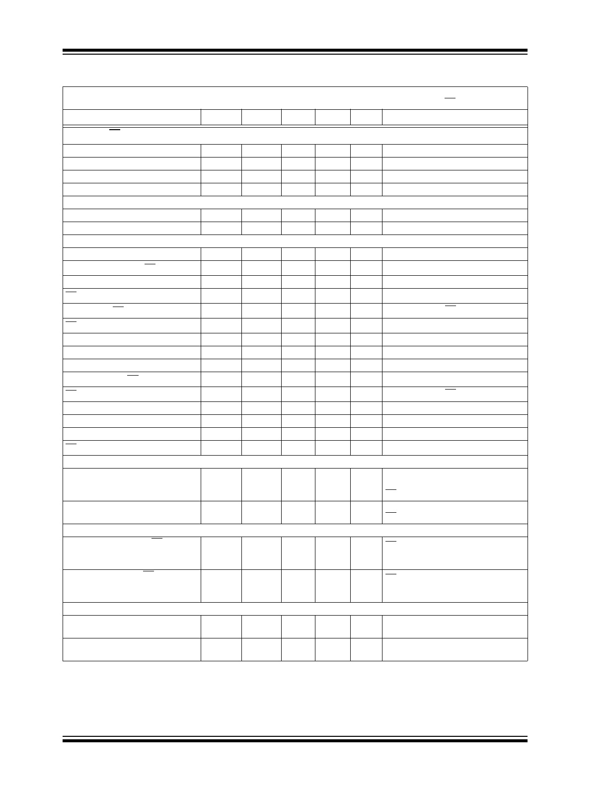
DIGITAL CHARACTERISTICS
Electrical Specifications: Unless otherwise indicated, T
A
= +25°C, V
DD
= +2.5V to +5.5V, V
SS
= GND, V
REF
= V
SS
, G = +1 V/V,
Input = CH0 = (0.3V)/G, CH1 to CH7 = 0.3V, R
L
= 10 k
to V
DD
/2, C
L
= 60 pF, SI and SCK are tied low, and CS is tied high.
Parameters
Sym
Min
Typ
Max
Units
Conditions
SPI Inputs (CS, SI, SCK)
Logic Threshold, Low
V
IL
0
—
0.3V
DD
V
Input Leakage Current
I
IL
-1.0
—
+1.0
µA
Logic Threshold, High
V
IH
0.7V
DD
—
V
DD
V
Amplifier Output Leakage Current
—
-1.0
—
+1.0
µA
In Shutdown mode
SPI Output (SO, for MCP6S26 and MCP6S28)
Logic Threshold, Low
V
OL
V
SS
—
V
SS
+0.4
V
I
OL
= 2.1 mA, V
DD
= 5V
Logic Threshold, High
V
OH
V
DD
-0.5
—
V
DD
V
I
OH
= -400 µA
SPI Timing
Pin Capacitance
C
PIN
—
10
—
pF
All digital I/O pins
Input Rise/Fall Times (CS, SI, SCK)
t
RFI
—
—
2
µs
Note 1
Output Rise/Fall Times (SO)
t
RFO
—
5
—
ns
MCP6S26 and MCP6S28
CS high time
t
CSH
40
—
—
ns
SCK edge to CS fall setup time
t
CS0
10
—
—
ns
SCK edge when CS is high
CS fall to first SCK edge setup time
t
CSSC
40
—
—
ns
SCK Frequency
f
SCK
—
—
10
MHz
V
DD
= 5V (Note 2)
SCK high time
t
HI
40
—
—
ns
SCK low time
t
LO
40
—
—
ns
SCK last edge to CS rise setup time
t
SCCS
30
—
—
ns
CS rise to SCK edge setup time
t
CS1
100
—
—
ns
SCK edge when CS is high
SI set-up time
t
SU
40
—
—
ns
SI hold time
t
HD
10
—
—
ns
SCK to SO valid propagation delay
t
DO
—
—
80
ns
MCP6S26 and MCP6S28
CS rise to SO forced to zero
t
SOZ
—
—
80
ns
MCP6S26 and MCP6S28
Channel and Gain Select Timing
Channel Select Time
t
CH
—
1.5
—
µs
CHx = 0.6V, CHy =0.3V, G = 1,
CHx to CHy select
CS = 0.7V
DD
to V
OUT
90% point
Gain Select Time
t
G
—
1
—
µs
CHx = 0.3V, G = 5 to G = 1 select,
CS = 0.7V
DD
to V
OUT
90% point
Shutdown Mode Timing
Out of Shutdown mode (CS goes
high) to Amplifier Output Turn-on
Time
t
ON
—
3.5
10
µs
CS = 0.7V
DD
to V
OUT
90% point
Into Shutdown mode (CS goes high)
to Amplifier Output High-Z Turn-off
Time
t
OFF
—
1.5
—
µs
CS = 0.7V
DD
to V
OUT
90% point
POR Timing
Power-On Reset power-up time
t
RPU
—
30
—
µs
V
DD
= V
POR
- 0.1V to V
POR
+ 0.1V,
50% V
DD
to 90% V
OUT
point
Power-On Reset power-down time
t
RPD
—
10
—
µs
V
DD
= V
POR
+ 0.1V to V
POR
- 0.1V,
50% V
DD
to 90% V
OUT
point
Note
1: Not tested in production. Set by design and characterization.
2: When using the device in the daisy chain configuration, maximum clock frequency is determined by a combination of
propagation delay time (t
DO
80 ns), data input setup time (t
SU
40 ns), SCK high time (t
HI
40 ns), and SCK rise and
fall times of 5 ns. Maximum f
SCK
is, therefore,
5.8 MHz.
2003-2012 Microchip Technology Inc.
DS21117B-page 5
MCP6S21/2/6/8
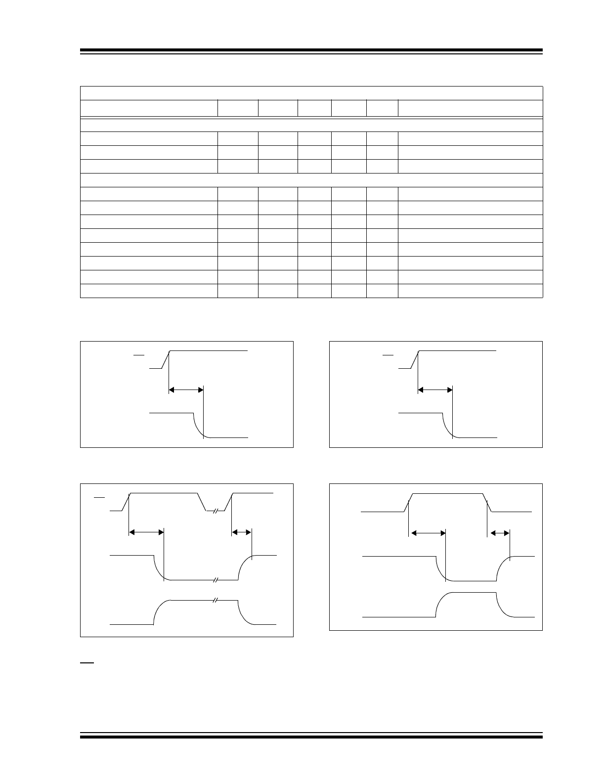
TEMPERATURE CHARACTERISTICS
FIGURE 1-1:
Channel Select Timing
Diagram.
FIGURE 1-2:
PGA Shutdown timing
diagram (must enter correct commands before
CS goes high).
FIGURE 1-3:
Gain Select Timing
Diagram.
FIGURE 1-4:
POR power-up and power-
down timing diagram.
Electrical Specifications: Unless otherwise indicated, V
DD
= +2.5V to +5.5V, V
SS
= GND.
Parameters
Sym
Min
Typ
Max
Units
Conditions
Temperature Ranges
Specified Temperature Range
T
A
-40
—
+85
°C
Operating Temperature Range
T
A
-40
—
+125
°C
(Note 1)
Storage Temperature Range
T
A
-65
—
+150
°C
Thermal Package Resistances
Thermal Resistance, 8L-PDIP
JA
—
85
—
°C/W
Thermal Resistance, 8L-SOIC
JA
—
163
—
°C/W
Thermal Resistance, 8L-MSOP
JA
—
206
—
°C/W
Thermal Resistance, 14L-PDIP
JA
—
70
—
°C/W
Thermal Resistance, 14L-SOIC
JA
—
120
—
°C/W
Thermal Resistance, 14L-TSSOP
JA
—
100
—
°C/W
Thermal Resistance, 16L-PDIP
JA
—
70
—
°C/W
Thermal Resistance, 16L-SOIC
JA
—
90
—
°C/W
Note 1: The MCP6S21/2/6/8 family of PGAs operates over this extended temperature range, but with reduced
performance. Operation in this range must not cause T
J
to exceed the Maximum Junction Temperature
(150°C).
CS
V
OUT
t
CH
0.6V
0.3V
CS
t
OFF
V
OUT
t
ON
Hi-Z
Hi-Z
I
SS
500 nA (typ)
1.0 mA (typ)
0.3V
CS
V
OUT
t
G
1.5V
0.3V
V
DD
t
RPD
V
OUT
t
RPU
Hi-Z
Hi-Z
V
POR
- 0.1V
V
POR
- 0.1V
V
POR
+ 0.1V
0.3V
I
SS
500 nA (typ)
1.0 mA (typ)
MCP6S21/2/6/8
DS21117B-page 6
2003-2012 Microchip Technology Inc.
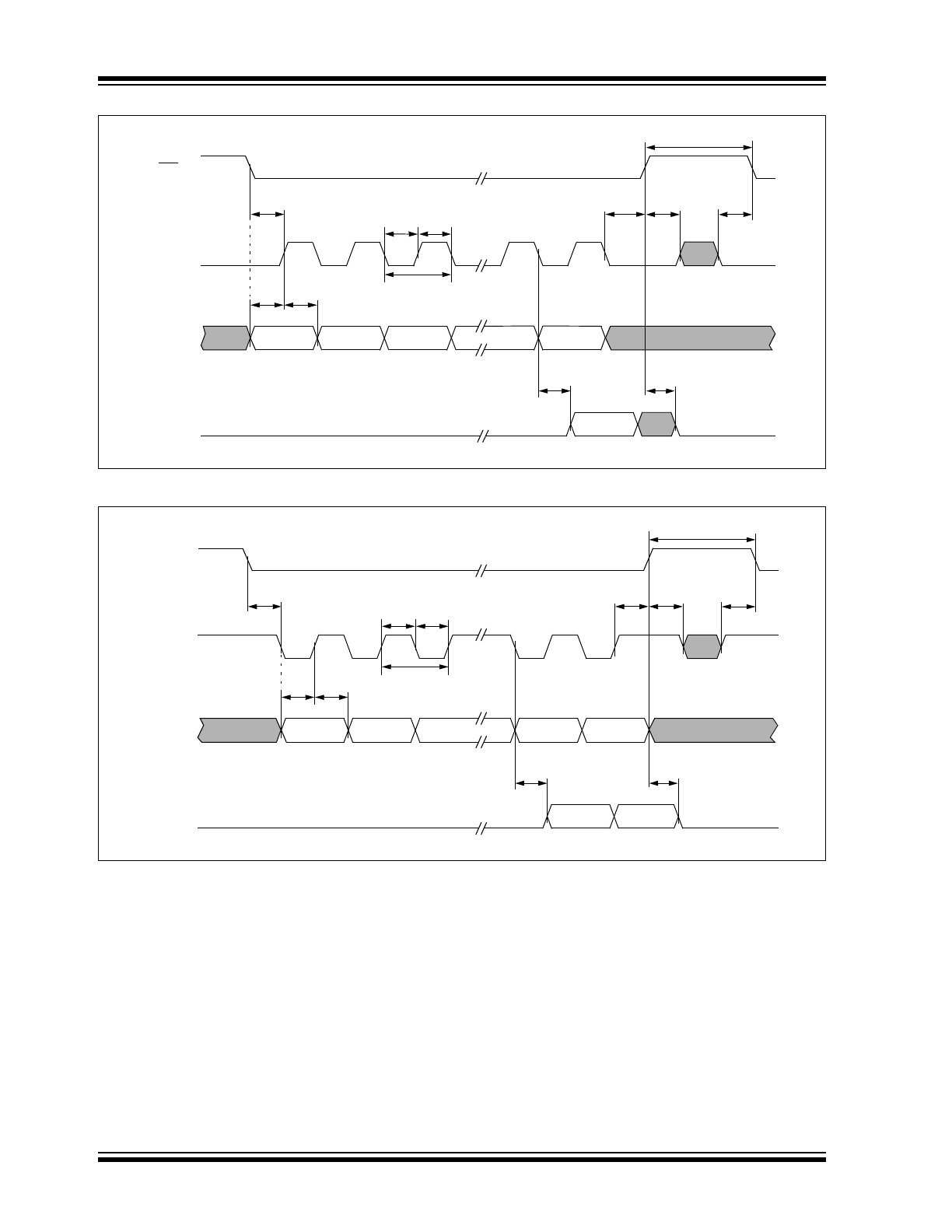
FIGURE 1-5:
Detailed SPI Serial Interface Timing, SPI 0,0 mode.
FIGURE 1-6:
Detailed SPI Serial Interface Timing, SPI 1,1 mode.
CS
SCK
SI
t
SU
t
HD
t
CSSC
t
SCCS
t
CSH
SO
(first 16 bits out are always zeros)
t
DO
t
SOZ
t
LO
t
HI
1/f
SCK
t
CS0
t
CS1
CS
SCK
SI
t
SU
t
HD
t
CSSC
t
SCCS
SO
(first 16 bits out are always zeros)
t
DO
t
SOZ
t
HI
t
LO
1/f
SCK
t
CS1
t
CSH
t
CS0
2003-2012 Microchip Technology Inc.
DS21117B-page 7
MCP6S21/2/6/8
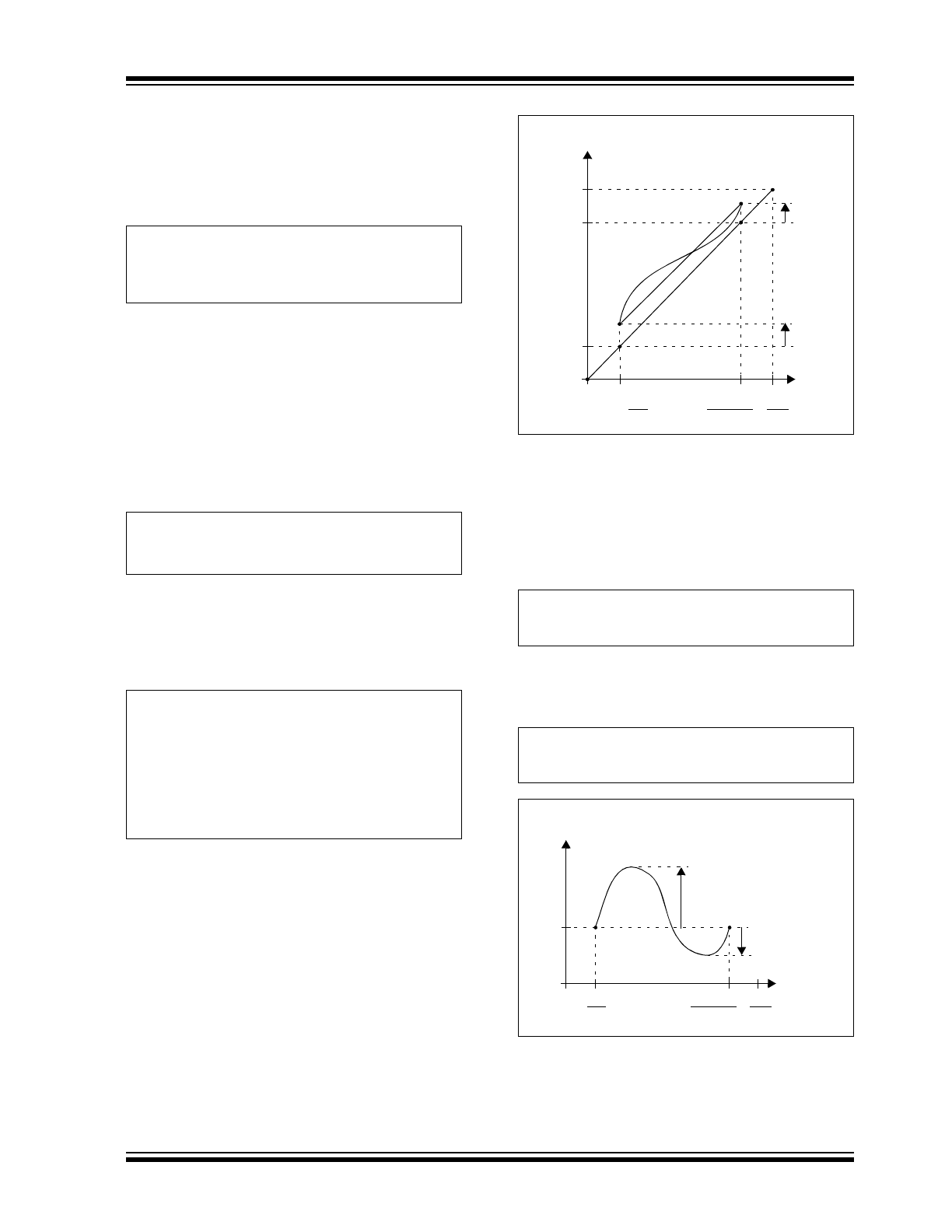
1.1
DC Output Voltage Specs / Model
1.1.1
IDEAL MODEL
The ideal PGA output voltage (V
OUT
) is:
EQUATION
(see Figure 1-7). This equation holds when there are
no gain or offset errors and when the V
REF
pin is tied to
a low impedance source (<< 0.1
) at ground potential
(V
SS
= 0V).
1.1.2
LINEAR MODEL
The PGA’s linear region of operation, including offset
and gain errors, is modeled by the line V
O_linear
, shown
in Figure 1-7.
EQUATION
The endpoints of this line are at V
O_ideal
= 0.3V and
V
DD
-0.3V. The gain and offset specifications referred to
in the electrical specifications are related to Figure 1-7,
as follows:
EQUATION
FIGURE 1-7:
Output Voltage Model with
the standard condition V
REF
= V
SS
= 0V.
1.1.3
OUTPUT NON-LINEARITY
Figure 1-8 shows the Integral Non-Linearity (INL) of the
output voltage.
EQUATION
The output non-linearity specification in the electrical
specifications is related to Figure 1-8 by:
EQUATION
FIGURE 1-8:
Output Voltage INL with the
standard condition V
REF
= V
SS
= 0V.
V
O_ideal
GV
IN
=
V
REF
V
SS
0V
=
=
where: G is the nominal gain
V
O_linear
G 1
g
E
+
V
IN
0.3V
V
OS
+
–
0.3V
+
=
V
REF
V
SS
0V
=
=
g
E
100%
V
2
V
1
–
G V
DD
0.6V
–
--------------------------------------
=
V
OS
V
1
G 1
g
E
+
-------------------------
=
G
T
A
g
E
T
A
----------
=
G
+1
=
0
0
0.3
V
DD
-0.3
V
DD
V
O
U
T
V
OUT
(V)
V
IN
(V)
0.3
V
DD
- 0.3 V
DD
G
G
G
V
1
V
O
_i
de
al
V
O
_l
in
ea
r
V
2
INL
V
OUT
V
O_linear
–
=
V
ONL
max V
4
V
3
V
DD
0.6V
–
---------------------------------
=
0
V
3
V
4
INL (V)
V
IN
(V)
0.3
V
DD
- 0.3 V
DD
G
G
G
0

MCP6S21/2/6/8
DS21117B-page 8
2003-2012 Microchip Technology Inc.
1.1.4
DIFFERENT V
REF
CONDITIONS
Some of the plots in Section 2.0, “Typical Performance
Curves”, have the conditions V
REF
= V
DD
/2 or
V
REF
= V
DD
. The equations and figures above are eas-
ily modified for these conditions. The ideal V
OUT
becomes:
EQUATION
The complete linear model is:
EQUATION
where the new V
IN
endpoints are:
EQUATION
The equations for extracting the specifications do not
change.
V
O_ideal
V
REF
G V
IN
V
REF
–
+
=
V
DD
V
REF
V
SS
0V
=
V
O_linear
G 1
g
E
+
V
IN
V
IN_L
V
OS
+
–
0.3V
+
=
V
IN_L
0.3V
V
REF
–
G
V
REF
+
------------------------------
=
V
IN_R
V
DD
0.3V
–
V
REF
–
G
V
R EF
+
-----------------------------------------------
=
2003-2012 Microchip Technology Inc.
DS21117B-page 9
MCP6S21/2/6/8
2.0
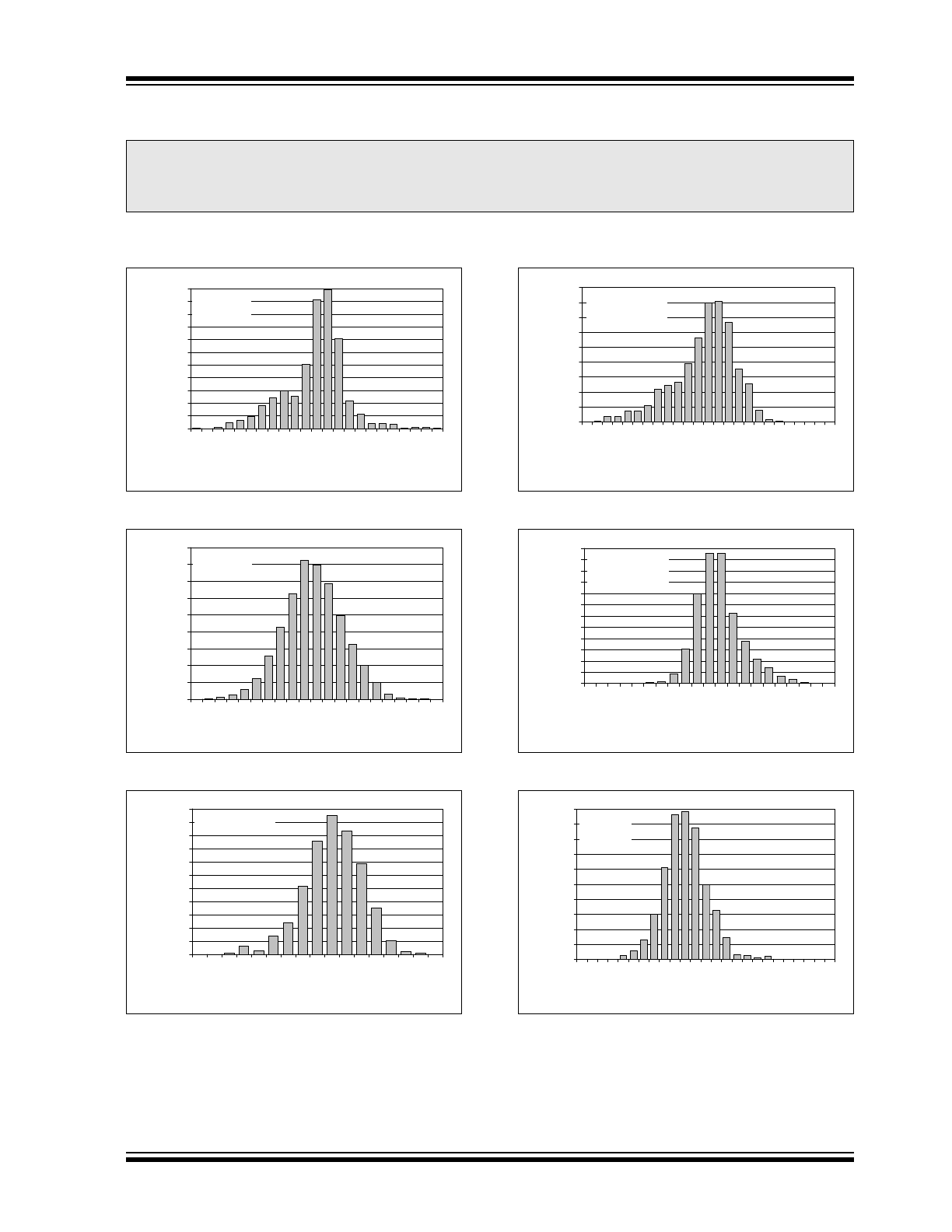
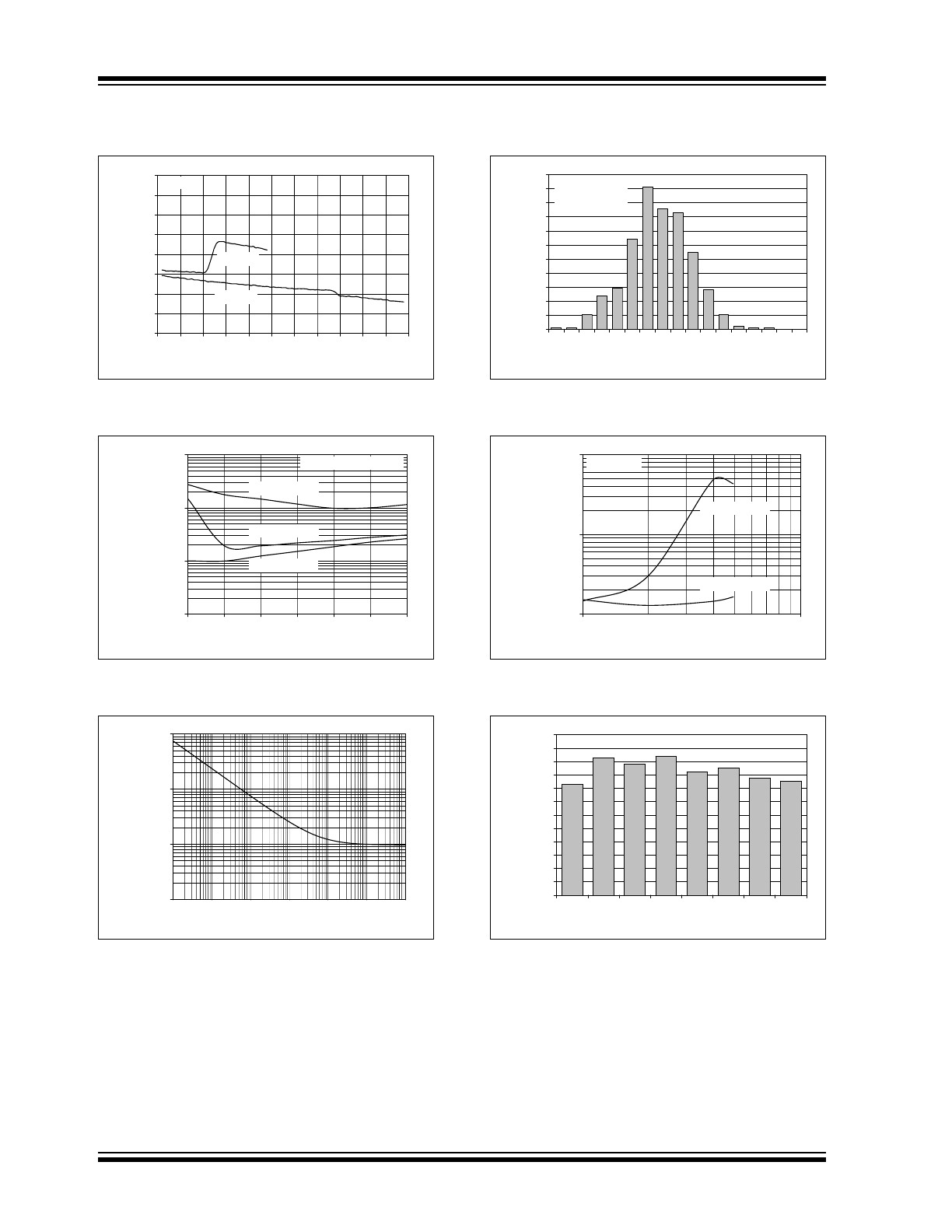
TYPICAL PERFORMANCE CURVES
Note: Unless otherwise indicated, T
A
= +25°C, V
DD
= +5.0V, V
SS
= GND, V
REF
= V
SS
, G= +1 V/V,
Input = CH0 = (0.3V)/G, CH1 to CH7 = 0.3V, R
L
= 10 k
to V
DD
/2, and C
L
= 60 pF.
FIGURE 2-1:
DC Gain Error, G = +1.
FIGURE 2-2:
DC Gain Error, G
+2.
FIGURE 2-3:
Ladder Resistance Drift.
FIGURE 2-4:
DC Gain Drift, G = +1.
FIGURE 2-5:
DC Gain Drift, G
+2.
FIGURE 2-6:
Input Offset Voltage,
V
DD
= 4.0V.
Note:
The graphs and tables provided following this note are a statistical summary based on a limited number of
samples and are provided for informational purposes only. The performance characteristics listed herein
are not tested or guaranteed. In some graphs or tables, the data presented may be outside the specified
operating range (e.g., outside specified power supply range) and therefore outside the warranted range.
0%
2%
4%
6%
8%
10%
12%
14%
16%
18%
20%
22%
-0.
040
-0.
036
-0.
032
-0.
028
-0.
024
-0.
020
-0.
016
-0.
012
-0.
008
-0.
004
0.
000
0.
004
DC Gain Error (%)
P
e
rcentage of Occur
re
nces
420 Samples
G = +1
0%
2%
4%
6%
8%
10%
12%
14%
16%
18%
-0.5
-0.4
-0.3
-0.2
-0.1
0.0
0.1
0.2
0.3
0.4
0.5
DC Gain Error (%)
Percentage of Occurrences
420 Samples
G
t +2
0%
2%
4%
6%
8%
10%
12%
14%
16%
18%
20%
22%
0.
023
0.
024
0.
025
0.
026
0.
027
0.
028
0.
029
0.
030
0.
031
Ladder Resistance Drift (%/°C)
P
e
rcentage of Occur
re
nces
420 Samples
T
A
= -40 to +125°C
0%
2%
4%
6%
8%
10%
12%
14%
16%
18%
-0
.0006
-0
.0005
-0
.0004
-0
.0003
-0
.0002
-0
.0001
0.0000
0.0001
0.0002
0.0003
0.0004
0.0005
0.0006
DC Gain Drift (%/°C)
P
e
rcent
a
ge of
O
ccurrences
420 Samples
G = +1
T
A
= -40 to +125°C
0%
2%
4%
6%
8%
10%
12%
14%
16%
18%
20%
22%
24%
-0.0020
-0.0016
-0.0012
-0.0008
-0.0004
0.0000
0.0004
0.0008
0.0012
0.0016
0.0020
DC Gain Drift (%/°C)
Percentage of Occurrences
420 Samples
G
t +2
T
A
= -40 to +125°C
0%
2%
4%
6%
8%
10%
12%
14%
16%
18%
20%
-240
-200
-160
-120
-8
0
-4
0
0
40
80
120
160
200
240
Input Offset Voltage (µV)
P
e
rcentage of Occur
re
nces
360 Samples
V
DD
= 4.0 V
G = +1
MCP6S21/2/6/8
DS21117B-page 10
2003-2012 Microchip Technology Inc.
Note: Unless otherwise indicated, T
A
= +25°C, V
DD
= +5.0V, V
SS
= GND, V
REF
= V
SS
, G= +1 V/V,
Input = CH0 = (0.3V)/G, CH1 to CH7 = 0.3V, R
L
= 10 k
to V
DD
/2, and C
L
= 60 pF.
FIGURE 2-7:
Input Offset Voltage vs.
V
REF
Voltage.
FIGURE 2-8:
DC Output Non-Linearity vs.
Supply Voltage.
FIGURE 2-9:
Input Noise Voltage Density
vs. Frequency.
FIGURE 2-10:
Input Offset Voltage Drift.
FIGURE 2-11:
DC Output Non-Linearity vs.
Output Swing.
FIGURE 2-12:
Input Noise Voltage Density
vs. Gain.
-200
-150
-100
-50
0
50
100
150
200
0.0
0.5
1.0
1.5
2.0
2.5
3.0
3.5
4.0
4.5
5.0
5.5
V
REF
Voltage (V)
Input O
ffset V
o
lt
age (µV
)
V
DD
= +5.5
V
DD
= +2.5
G = +1
0.00001
0.0001
0.001
0.01
2.5
3.0
3.5
4.0
4.5
5.0
5.5
Power Supply Voltage (V)
DC Output Non-Linearity,
Input Referred (% of FSR)
V
ONL
/G, G = +1
V
ONL
/G, G = +2
V
ONL
/G, G
t +4
V
OUT
= 0.3V to V
DD
-0.3V
1
10
100
1000
0.1
1
10
100
1000
10000
100000
Frequency (Hz)
Input Noise Voltage Density
(nV/
Hz)
1k
10k
100k
1
10
100
0.1
0%
2%
4%
6%
8%
10%
12%
14%
16%
18%
20%
22%
-1
6
-1
4
-1
2
-1
0
-8
-6
-4
-2
0
2
4
6
8
10
12
14
16
Input Offset Voltage Drift (µV/°C)
P
e
rcentage of Occur
re
nces
420 Samples
T
A
= -40 to +125°C
G = +1
0.0001%
0.0010%
0.0100%
1
10
Output Voltage Swing (V
P-P
)
DC Output Non-Linearity,
Input Referred (%)
V
ONL
/G, G
t +2
V
ONL
/G, G = +1
V
DD
= +5.5 V
0
1
2
3
4
5
6
7
8
9
10
11
12
1
2
4
5
8
10
16
32
Gain (V/V)
Input Noise Voltage Density
(nV/
Hz)
f = 10 kHz