
1994-2012 Microchip Technology Inc.
DS21095K-page 1
24LC21
Features:
• Single supply with operation down to 2.5V
• Completely implements DDC1
™
/DDC2
™
interface
for monitor identification
• Low-power CMOS technology:
- 1 mA active current typical
- 10
A standby current typical at 5.5V
• 2-wire serial interface bus, I
2
C
™
compatible
• Self-timed write cycle (including auto-erase)
• Page-write buffer for up to 8 bytes
• 100 kHz (2.5V) and 400 kHz (5V) compatibility
• Factory programming (QTP) available
• 1,000,000 erase/write cycles ensured
• Data retention > 200 years
• 8-pin PDIP and SOIC package
• Available for extended temperature ranges
Description:
The Microchip Technology Inc. 24LC21 is a 128 x 8 bit
Electrically Erasable PROM. This device is designed
for use in applications requiring storage and serial
transmission of configuration and control information.
Two modes of operation have been implemented:
Transmit-only mode and Bidirectional mode. Upon
power-up, the device will be in the Transmit-only mode,
sending a serial bit stream of the entire memory array
contents, clocked by the V
CLK
pin. A valid high-to-low
transition on the SCL pin will cause the device to enter
the Bidirectional mode, with byte selectable read/write
capability of the memory array. The 24LC21 is available
in a standard 8-pin PDIP and SOIC package, in both
commercial and industrial temperature ranges.
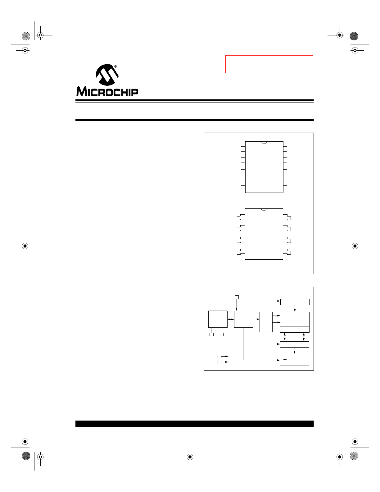
Package Types
Block Diagram
Commercial (C):
0°C to +70°C
Industrial (I):
-40°C to +85°C
24L
C21
NC
NC
NC
V
SS
1
2
3
4
8
7
6
5
V
CC
V
CLK
SCL
SDA
24
L
C
21
NC
NC
NC
V
SS
1
2
3
4
8
7
5
5
V
CC
V
CLK
SCL
SDA
PDIP
SOIC
HV Generator
EEPROM
Array
Page Latches
YDEC
XDEC
Sense
Amp
R/W Control
Memory
Control
Logic
I/O
Control
Logic
V
CLK
SDA SCL
V
CC
V
SS
1K 2.5V Dual Mode I
2
C
™
Serial EEPROM
Not recommended for new designs –
Please use 24LCS21A.
21095K.book Page 1 Wednesday, December 5, 2012 2:28 PM
24LC21
DS21095K-page 2
1994-2012 Microchip Technology Inc.
1.0
ELECTRICAL CHARACTERISTICS
Absolute Maximum Ratings
(†)
V
CC
.............................................................................................................................................................................7.0V
All inputs and outputs w.r.t. V
SS
........................................................................................................ -0.6V to V
CC
+ 1.0V
Storage temperature ...............................................................................................................................-65°C to +150°C
Ambient temperature with power applied ................................................................................................-40°C to +125°C
Soldering temperature of leads (10 seconds) ....................................................................................................... +300°C
ESD protection on all pins
4 kV
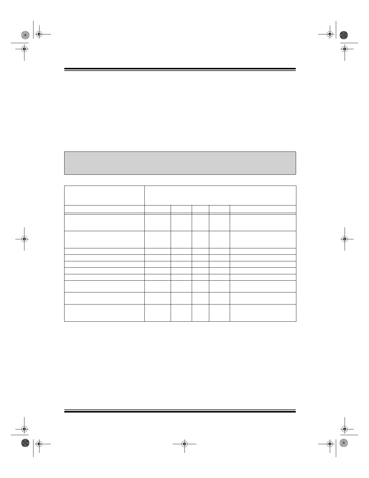
TABLE 1-1:
DC CHARACTERISTICS
† NOTICE: Stresses above those listed under “Absolute Maximum Ratings” may cause permanent damage to the
device. This is a stress rating only and functional operation of the device at these or any other conditions above those
indicated in the operational listings of this specification is not implied. Exposure to Absolute Maximum Rating
conditions for extended periods may affect device reliability.
DC CHARACTERISTICS
V
CC
= +2.5V to 5.5V
Commercial
(C): T
A
= 0°C to +70°C
Industrial (I):
T
A
= -40°C to +85°C
Parameter
Symbol
Min
Max
Units
Conditions
SCL and SDA pins:
High-level input voltage
Low-level input voltage
V
IH
V
IL
.7 V
CC
—
—
.3 V
CC
V
V
—
—
Input levels on V
CLK
pin:
High-level input voltage
Low-level input voltage
V
IH
V
IL
2.0
—
.8
.2 V
CC
V
V
V
CC
2.7V (Note 1)
V
CC
< 2.7V (Note 1)
Hysteresis of Schmitt Trigger inputs
V
HYS
.05 V
CC
—
V
(Note 1)
Low-level output voltage
V
OL1
—
.4
V
I
OL
= 3 mA, V
CC
= 2.5V (Note 1)
Low-level output voltage
V
OL2
—
.6
V
I
OL
= 6 mA, V
CC
= 2.5V
Input leakage current
I
LI
-10
10
A
V
IN
= .1V to V
CC
Output leakage current
I
LO
-10
10
A
V
OUT
= .1V to V
CC
Pin capacitance (all inputs/outputs)
C
IN
, C
OUT
—
10
pF
V
CC
= 5.0V (Note1),
T
A
= 25
C, F
CLK
= 1 MHz
Operating current
I
CC
Write
I
CC
Read
—
—
3
1
mA
mA
V
CC
= 5.5V, SCL = 400 kHz
Standby current
I
CCS
—
—
30
100
A
A
V
CC
= 3.0V, SDA = SCL = V
CC
V
CC
= 5.5V, SDA = SCL = V
CC
(Note 2)
Note 1:
This parameter is periodically sampled and not 100% tested.
2:
V
LCK
must be grounded.
21095K.book Page 2 Wednesday, December 5, 2012 2:28 PM
1994-2012 Microchip Technology Inc.
DS21095K-page 3
24LC21
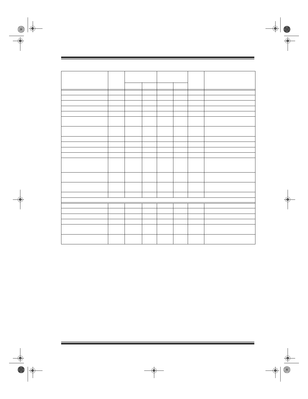
TABLE 1-2:
AC CHARACTERISTICS
Parameter
Symbol
Standard Mode
Vcc= 4.5 - 5.5V
Fast Mode
Units
Remarks
Min
Max
Min
Max
Clock frequency
F
CLK
—
100
—
400
kHz
—
Clock high time
T
HIGH
4000
—
600
—
ns
—
Clock low time
T
LOW
4700
—
1300
—
ns
—
SDA and SCL rise time
T
R
—
1000
—
300
ns
(Note 1)
SDA and SCL fall time
T
F
—
300
—
300
ns
(Note 1)
Start condition hold time
T
HD
:
STA
4000
—
600
—
ns
After this period the first clock
pulse is generated
Start condition setup time
T
SU
:
STA
4700
—
600
—
ns
Only relevant for repeated
Start condition
Data input hold time
T
HD
:
DAT
0
—
0
—
ns
(Note 2)
Data input setup time
T
SU
:
DAT
250
—
100
—
ns
—
Stop condition setup time
T
SU
:
STO
4000
—
600
—
ns
—
Output valid from clock
T
AA
—
3500
—
900
ns
(Note 2)
Bus free time
T
BUF
4700
—
1300
—
ns
Time the bus must be free
before a new transmission
can start
Output fall time from V
IH
min. to V
IL
max.
T
OF
—
250
20 + .1
C
B
250
ns
(Note 1), C
B
100 pF
Input filter spike suppres-
sion (SDA and SCL pins)
T
SP
—
50
—
50
ns
(Note 3)
Write cycle time
T
WR
—
10
—
10
ms
Byte or Page mode
Transmit-only Mode Parameters
Output valid from V
CLK
T
VAA
—
2000
—
1000
ns
—
V
CLK
high time
T
VHIGH
4000
—
600
—
ns
—
V
CLK
low time
T
VLOW
4700
—
1300
—
ns
—
Mode transition time
T
VHZ
—
500
—
500
ns
—
Transmit-only power-up
time
T
VPU
0
—
0
—
ns
—
Endurance
—
1M
—
1M
—
cycles 25°C,
V
CC
= 5.0V, Block
mode (Note 4)
Note 1:
Not 100% tested. C
B
= total capacitance of one bus line in pF.
2:
As a transmitter, the device must provide an internal minimum delay time to bridge the undefined region
(minimum 300 ns) of the falling edge of SCL to avoid unintended generation of Start or Stop conditions.
3:
The combined T
SP
and V
HYS
specifications are due to new Schmitt Trigger inputs which provide improved
noise and spike suppression. This eliminates the need for a T
I
specification for standard operation.
4:
This parameter is not tested but ensured by characterization. For endurance estimates in a specific
application, please consult the Total Endurance
™
Model which can be obtained from Microchip’s web site
at: www.microchip.com
21095K.book Page 3 Wednesday, December 5, 2012 2:28 PM
24LC21
DS21095K-page 4
1994-2012 Microchip Technology Inc.
2.0
FUNCTIONAL DESCRIPTION
The 24LC21 operates in two modes, the Transmit-only
mode and the Bidirectional mode. There is a separate
two-wire protocol to support each mode, each having a
separate clock input and sharing a common data line
(SDA). The device enters the Transmit-only mode upon
power-up. In this mode, the device transmits data bits
on the SDA pin in response to a clock signal on the
V
CLK
pin. The device will remain in this mode until a
valid high-to-low transition is placed on the SCL input.
When a valid transition on SCL is recognized, the
device will switch into the Bidirectional mode. The only
way to switch the device back to the Transmit-only
mode is to remove power from the device.
2.1
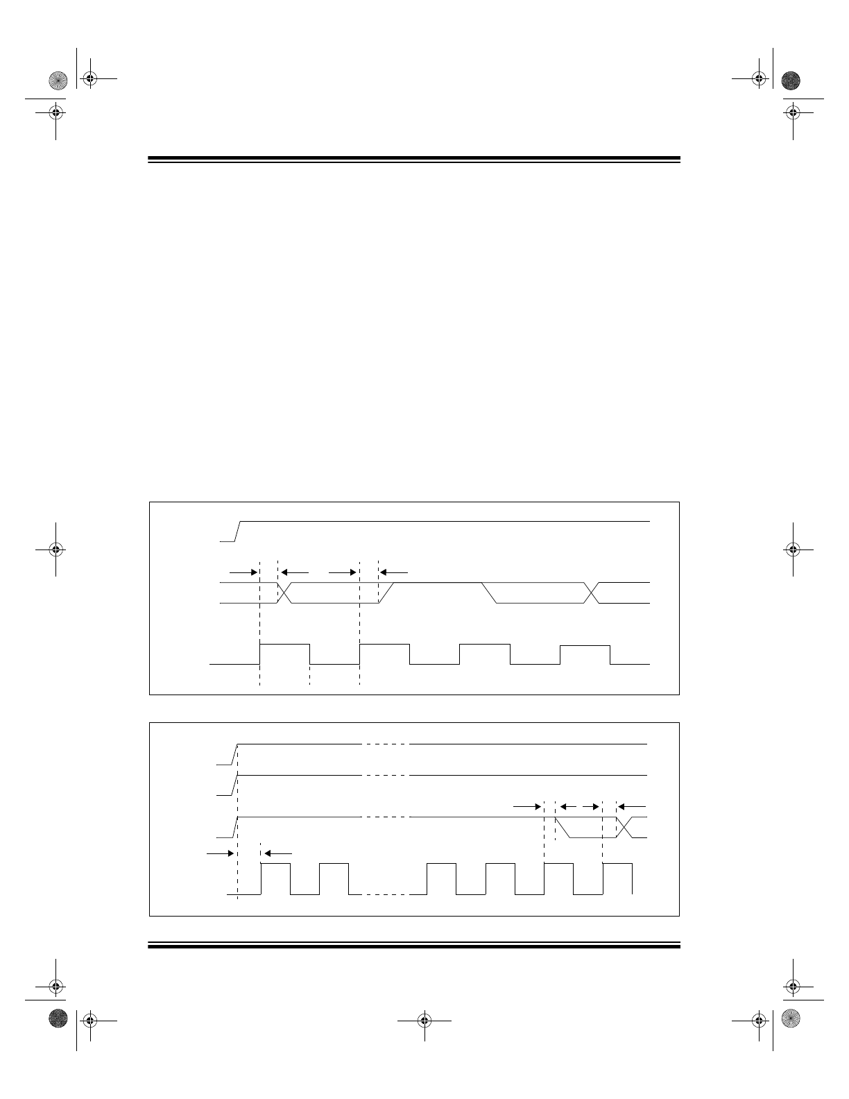
Transmit-only Mode
The device will power-up in the Transmit-only mode.
This mode supports a unidirectional two-wire protocol
for transmission of the contents of the memory array.
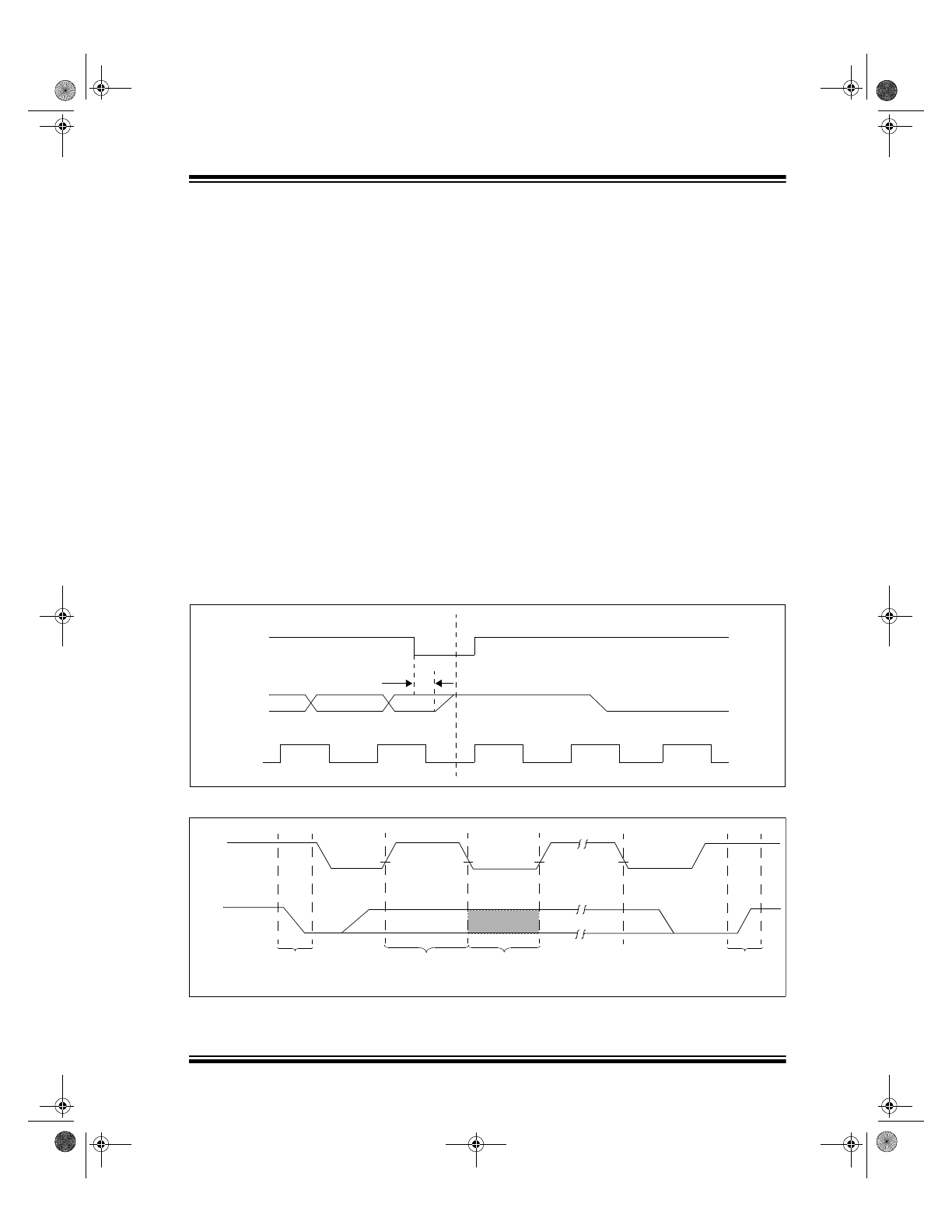
This device requires that it be initialized prior to valid
data being sent in the Transmit-only mode (see Initial-
ization Procedure, below). In this mode, data is trans-
mitted on the SDA pin in 8-bit bytes, each followed by
a ninth, null bit (see Figure 2-1). The clock source for
the Transmit-only mode is provided on the V
CLK
pin,
and a data bit is output on the rising edge on this pin.
The eight bits in each byte are transmitted Most Signif-
icant bit first. Each byte within the memory array will be
output in sequence. When the last byte in the memory
array is transmitted, the output will wrap around to the
first location and continue. The Bidirectional mode
Clock (SCL) pin must be held high for the device to
remain in the Transmit-only mode.
2.2
Initialization Procedure
After V
CC
has stabilized, the device will be in the Trans-
mit-only mode. Nine clock cycles on the V
CLK
pin must
be given to the device for it to perform internal synchro-
nization. During this period, the SDA pin will be in a
high-impedance state. On the rising edge of the tenth
clock cycle, the device will output the first valid data bit
which will be the Most Significant bit of a byte. The
device will power-up at an indeterminate byte address.
(Figure 2-2).
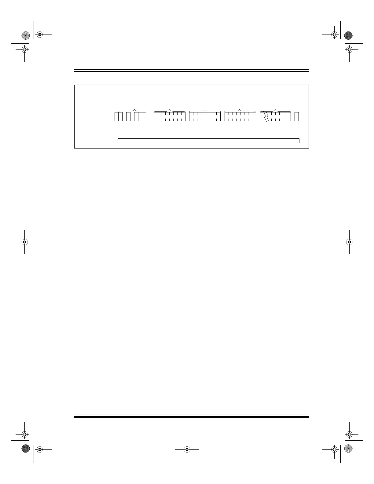
FIGURE 2-1:
TRANSMIT-ONLY MODE
FIGURE 2-2:
DEVICE INITIALIZATION
SCL
SDA
V
CLK
T
VAA
T
VAA
Bit 1 (LSB)
Null Bit
Bit 1 (MSB)
Bit 7
T
VLOW
T
VHIGH
T
VAA
T
VAA
Bit 8
Bit 7
High-impedance for 9 clock cycles
T
VPU
1
2
8
9
10
11
SCL
SDA
V
CLK
V
CC
21095K.book Page 4 Wednesday, December 5, 2012 2:28 PM
1994-2012 Microchip Technology Inc.
DS21095K-page 5
24LC21
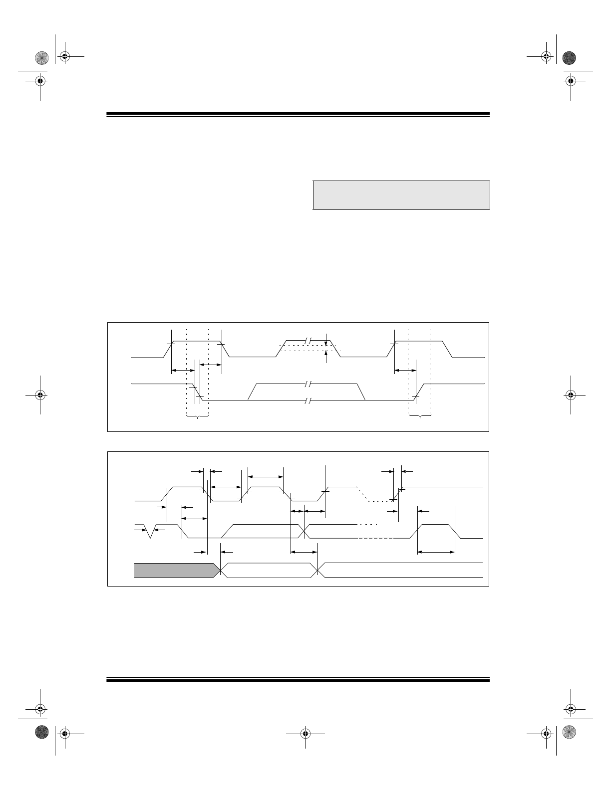
3.0
BIDIRECTIONAL MODE
The 24LC21 can be switched into the Bidirectional
mode (see Figure 3-1) by applying a valid high-to-low
transition on the Bidirectional mode clock (SCL). When
the device has been switched into the Bidirectional
mode, the V
CLK
input is disregarded, with the exception
that a logic high level is required to enable write capa-
bility. This mode supports a two-wire bidirectional data
transmission protocol. In this protocol, a device that
sends data on the bus is defined to be the transmitter,
and a device that receives data from the bus is defined
to be the receiver. The bus must be controlled by a
master device that generates the Bidirectional mode
clock (SCL), controls access to the bus and generates
the Start and Stop conditions, while the 24LC21 acts as
the slave. Both master and slave can operate as
transmitter or receiver, but the master device
determines which mode is activated.
3.1
Bidirectional Mode Bus
Characteristics
The following bus protocol has been defined:
• Data transfer may be initiated only when the bus
is not busy.
• During data transfer, the data line must remain
stable whenever the clock line is high. Changes in
the data line while the clock line is high will be
interpreted as a Start or Stop condition.
Accordingly, the following bus conditions have been
defined (see Figure 3-2).
3.1.1
BUS NOT BUSY (A)
Both data and clock lines remain high.
3.1.2
START DATA TRANSFER (B)
A high-to-low transition of the SDA line while the clock
(SCL) is high determines a Start condition. All
commands must be preceded by a Start condition.
3.1.3
STOP DATA TRANSFER (C)
A low-to-high transition of the SDA line while the clock
(SCL) is high determines a Stop condition. All
operations must be ended with a Stop condition.
FIGURE 3-1:
MODE TRANSITION
FIGURE 3-2:
DATA TRANSFER SEQUENCE ON THE SERIAL BUS
SCL
SDA
V
CLK
Bidirectional mode
T
VHZ
Transmit-only mode
(A)
(B)
(D)
(D)
(A)
(C)
Start
Condition
Address
or
Acknowledge
Valid
Data
Allowed
to Change
Stop
Condition
SCL
SDA
21095K.book Page 5 Wednesday, December 5, 2012 2:28 PM
24LC21
DS21095K-page 6
1994-2012 Microchip Technology Inc.
3.1.4
DATA VALID (D)
The state of the data line represents valid data when,
after a Start condition, the data line is stable for the
duration of the high period of the clock signal.
The data on the line must be changed during the low
period of the clock signal. There is one clock pulse per
bit of data.
Each data transfer is initiated with a Start condition and
terminated with a Stop condition. The number of the
data bytes transferred between the Start and Stop
conditions is determined by the master device and is
theoretically unlimited, although only the last eight will
be stored when doing a write operation. When an
overwrite does occur, it will replace data in a first in first
out fashion.
3.1.5
ACKNOWLEDGE
Each receiving device, when addressed, is obliged to
generate an acknowledge after the reception of each
byte. The master device must generate an extra clock
pulse which is associated with this Acknowledge bit.
The device that acknowledges has to pull down the
SDA line during the acknowledge clock pulse in such a
way that the SDA line is stable low during the high
period of the acknowledge related clock pulse. Of
course, setup and hold times must be taken into
account. A master must signal an end of data to the
slave by not generating an Acknowledge bit on the last
byte that has been clocked out of the slave. In this
case, the slave must leave the data line high to enable
the master to generate the Stop condition.
FIGURE 3-3:
BUS TIMING START/STOP
FIGURE 3-4:
BUS TIMING DATA
Note:
The 24LC21 does not generate any
Acknowledge bits if an internal program-
ming cycle is in progress.
T
SU
:
STA
T
HD
:
STA
V
HYS
T
SU
:
STO
Start
Stop
SCL
SDA
T
SU
:
STA
T
F
T
LOW
T
HIGH
T
R
T
HD
:
DAT
T
SU
:
DAT
T
SU
:
STO
T
HD
:
STA
T
BUF
T
AA
T
AA
T
SP
T
HD
:
STA
SCL
SDA
IN
SDA
OUT
21095K.book Page 6 Wednesday, December 5, 2012 2:28 PM
1994-2012 Microchip Technology Inc.
DS21095K-page 7
24LC21
3.1.6
SLAVE ADDRESS
After generating a Start condition, the bus master trans-
mits the slave address consisting of a 7-bit device code
‘1010’ for the 24LC21, followed by three “don’t care”
bits.
The eighth bit of slave address determines if the master
device wants to read or write to the 24LC21 (Figure 3-5).
The 24LC21 monitors the bus for its corresponding
slave address all the time. It generates an
Acknowledge bit if the slave address was true and it is
not in a programming mode.
FIGURE 3-5:
CONTROL BYTE
ALLOCATION
4.0
WRITE OPERATION
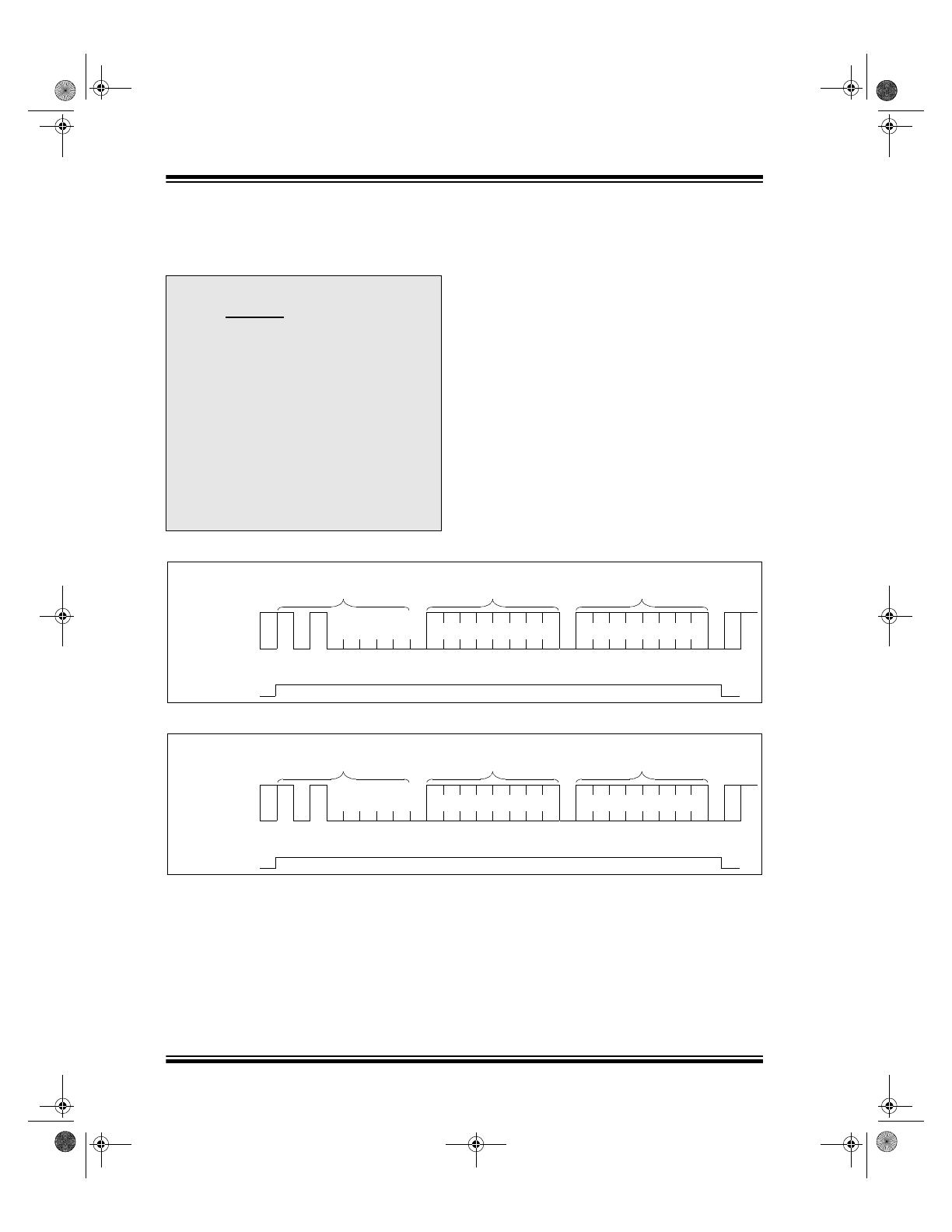
4.1
Byte Write
Following the Start signal from the master, the slave
address (4 bits), the “don’t care” bits (3 bits) and the
R/W bit which is a logic low, is placed onto the bus by
the master transmitter. This indicates to the
addressed slave receiver that a byte with a word
address will follow after it has generated an Acknowl-
edge bit during the ninth clock cycle. Therefore, the
next byte transmitted by the master is the word
address and will be written into the address pointer of
the 24LC21. After receiving another Acknowledge
signal from the 24LC21 the master device will transmit
the data word to be written into the addressed mem-
ory location. The 24LC21 acknowledges again and
the master generates a Stop condition. This initiates
the internal write cycle, and during this time the
24LC21 will not generate Acknowledge signals
(Figure 4-1).
It is required that V
CLK
be held at a logic high level in
order to program the device. This applies to byte write
and page write operation. Note that V
CLK
can go low
while the device is in its self-timed program operation
and not affect programming.
4.2
Page Write
The write control byte, word address and the first data
byte are transmitted to the 24LC21 in the same way as
in a byte write. But instead of generating a Stop condi-
tion the master transmits up to eight data bytes to the
24LC21, which are temporarily stored in the on-chip
page buffer and will be written into the memory after the
master has transmitted a Stop condition. After the
receipt of each word, the three lower order address
pointer bits are internally incremented by one. The
higher order five bits of the word address remains
constant. If the master should transmit more than eight
words prior to generating the Stop condition, the
address counter will roll over and the previously
received data will be overwritten. As with the byte write
operation, once the Stop condition is received an
internal write cycle will begin (Figure 4-3).
Operation
Control Code
Chip Select
R/W
Read
1010
xxx
1
Write
1010
xxx
0
SLAVE ADDRESS
1
0
1
0
x
x
x
R/W
A
Start
Read/Write
21095K.book Page 7 Wednesday, December 5, 2012 2:28 PM
24LC21
DS21095K-page 8
1994-2012 Microchip Technology Inc.
It is required that V
CLK
be held at a logic high level in
order to program the device. This applies to byte write
and page write operation. Note that V
CLK
can go low
while the device is in its self-timed program operation
and not affect programming.
FIGURE 4-1:
BYTE WRITE
FIGURE 4-2:
BYTE WRITE
Note:
Page write operations are limited to writing
bytes within a single physical page,
regardless of the number of bytes
actually being written. Physical page
boundaries start at addresses that are
integer multiples of the page buffer size (or
‘page size’) and end at addresses that are
integer multiples of [page size - 1]. If a
page Write command attempts to write
across a physical page boundary, the
result is that the data wraps around to the
beginning of the current page (overwriting
data previously stored there), instead of
being written to the next page as might be
expected. It is therefore necessary for the
application software to prevent page write
operations that would attempt to cross a
page boundary.
S
P
BUS ACTIVITY
MASTER
SDA LINE
BUS ACTIVITY
S
T
A
R
T
S
T
O
P
Control
Byte
Word
Address
Data
A
C
K
A
C
K
A
C
K
V
CLK
S
P
BUS ACTIVITY
MASTER
SDA LINE
BUS ACTIVITY
S
T
A
R
T
S
T
O
P
Control
Byte
Word
Address
Data
A
C
K
A
C
K
A
C
K
V
CLK
21095K.book Page 8 Wednesday, December 5, 2012 2:28 PM
1994-2012 Microchip Technology Inc.
DS21095K-page 9
24LC21
FIGURE 4-3:
PAGE WRITE
S
P
BUS ACTIVITY
MASTER
SDA LINE
BUS ACTIVITY
S
T
A
R
T
Control
Byte
Word
Address
Data (n)
Data (n + 15)
S
T
O
P
A
C
K
A
C
K
A
C
K
A
C
K
A
C
K
Data (n + 1)
V
CLK
21095K.book Page 9 Wednesday, December 5, 2012 2:28 PM
24LC21
DS21095K-page 10
1994-2012 Microchip Technology Inc.
5.0
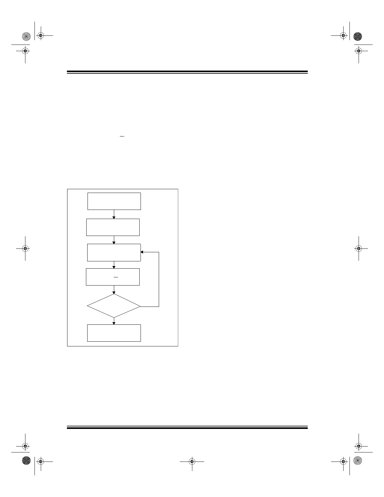
ACKNOWLEDGE POLLING
Since the device will not acknowledge during a write
cycle, this can be used to determine when the cycle is
complete (this feature can be used to maximize bus
throughput). Once the Stop condition for a Write
command has been issued from the master, the device
initiates the internally timed write cycle. ACK polling
can be initiated immediately. This involves the master
sending a Start condition followed by the control byte
for a Write command (R/W = 0). If the device is still
busy with the write cycle, then no ACK will be returned.
If the cycle is complete, then the device will return the
ACK and the master can then proceed with the next
Read or Write command. See Figure 5-1 for the flow
diagram.
FIGURE 5-1:
ACKNOWLEDGE
POLLING FLOW
6.0
WRITE PROTECTION
When using the 24LC21 in the Bidirectional mode, the
V
CLK
pin operates as the write-protect control pin.
Setting V
CLK
high allows normal write operations, while
setting V
CLK
low prevents writing to any location in the
array. Connecting the V
CLK
pin to V
SS
would allow the
24LC21 to operate as a serial ROM, although this
configuration would prevent using the device in the
Transmit-only mode.
Send
Write Command
Send Stop
Condition to
Initiate Write Cycle
Send Start
Send Control Byte
with R/W = 0
Did Device
Acknowledge
(ACK = 0)?
Next
Operation
No
Yes
21095K.book Page 10 Wednesday, December 5, 2012 2:28 PM
1994-2012 Microchip Technology Inc.
DS21095K-page 1
24LC21
Features:
• Single supply with operation down to 2.5V
• Completely implements DDC1
™
/DDC2
™
interface
for monitor identification
• Low-power CMOS technology:
- 1 mA active current typical
- 10
A standby current typical at 5.5V
• 2-wire serial interface bus, I
2
C
™
compatible
• Self-timed write cycle (including auto-erase)
• Page-write buffer for up to 8 bytes
• 100 kHz (2.5V) and 400 kHz (5V) compatibility
• Factory programming (QTP) available
• 1,000,000 erase/write cycles ensured
• Data retention > 200 years
• 8-pin PDIP and SOIC package
• Available for extended temperature ranges
Description:
The Microchip Technology Inc. 24LC21 is a 128 x 8 bit
Electrically Erasable PROM. This device is designed
for use in applications requiring storage and serial
transmission of configuration and control information.
Two modes of operation have been implemented:
Transmit-only mode and Bidirectional mode. Upon
power-up, the device will be in the Transmit-only mode,
sending a serial bit stream of the entire memory array
contents, clocked by the V
CLK
pin. A valid high-to-low
transition on the SCL pin will cause the device to enter
the Bidirectional mode, with byte selectable read/write
capability of the memory array. The 24LC21 is available
in a standard 8-pin PDIP and SOIC package, in both
commercial and industrial temperature ranges.
Package Types
Block Diagram
Commercial (C):
0°C to +70°C
Industrial (I):
-40°C to +85°C
24L
C21
NC
NC
NC
V
SS
1
2
3
4
8
7
6
5
V
CC
V
CLK
SCL
SDA
24
L
C
21
NC
NC
NC
V
SS
1
2
3
4
8
7
5
5
V
CC
V
CLK
SCL
SDA
PDIP
SOIC
HV Generator
EEPROM
Array
Page Latches
YDEC
XDEC
Sense
Amp
R/W Control
Memory
Control
Logic
I/O
Control
Logic
V
CLK
SDA SCL
V
CC
V
SS
1K 2.5V Dual Mode I
2
C
™
Serial EEPROM
Not recommended for new designs –
Please use 24LCS21A.
21095K.book Page 1 Wednesday, December 5, 2012 2:28 PM
24LC21
DS21095K-page 2
1994-2012 Microchip Technology Inc.
1.0
ELECTRICAL CHARACTERISTICS
Absolute Maximum Ratings
(†)
V
CC
.............................................................................................................................................................................7.0V
All inputs and outputs w.r.t. V
SS
........................................................................................................ -0.6V to V
CC
+ 1.0V
Storage temperature ...............................................................................................................................-65°C to +150°C
Ambient temperature with power applied ................................................................................................-40°C to +125°C
Soldering temperature of leads (10 seconds) ....................................................................................................... +300°C
ESD protection on all pins
4 kV
TABLE 1-1:
DC CHARACTERISTICS
† NOTICE: Stresses above those listed under “Absolute Maximum Ratings” may cause permanent damage to the
device. This is a stress rating only and functional operation of the device at these or any other conditions above those
indicated in the operational listings of this specification is not implied. Exposure to Absolute Maximum Rating
conditions for extended periods may affect device reliability.
DC CHARACTERISTICS
V
CC
= +2.5V to 5.5V
Commercial
(C): T
A
= 0°C to +70°C
Industrial (I):
T
A
= -40°C to +85°C
Parameter
Symbol
Min
Max
Units
Conditions
SCL and SDA pins:
High-level input voltage
Low-level input voltage
V
IH
V
IL
.7 V
CC
—
—
.3 V
CC
V
V
—
—
Input levels on V
CLK
pin:
High-level input voltage
Low-level input voltage
V
IH
V
IL
2.0
—
.8
.2 V
CC
V
V
V
CC
2.7V (Note 1)
V
CC
< 2.7V (Note 1)
Hysteresis of Schmitt Trigger inputs
V
HYS
.05 V
CC
—
V
(Note 1)
Low-level output voltage
V
OL1
—
.4
V
I
OL
= 3 mA, V
CC
= 2.5V (Note 1)
Low-level output voltage
V
OL2
—
.6
V
I
OL
= 6 mA, V
CC
= 2.5V
Input leakage current
I
LI
-10
10
A
V
IN
= .1V to V
CC
Output leakage current
I
LO
-10
10
A
V
OUT
= .1V to V
CC
Pin capacitance (all inputs/outputs)
C
IN
, C
OUT
—
10
pF
V
CC
= 5.0V (Note1),
T
A
= 25
C, F
CLK
= 1 MHz
Operating current
I
CC
Write
I
CC
Read
—
—
3
1
mA
mA
V
CC
= 5.5V, SCL = 400 kHz
Standby current
I
CCS
—
—
30
100
A
A
V
CC
= 3.0V, SDA = SCL = V
CC
V
CC
= 5.5V, SDA = SCL = V
CC
(Note 2)
Note 1:
This parameter is periodically sampled and not 100% tested.
2:
V
LCK
must be grounded.
21095K.book Page 2 Wednesday, December 5, 2012 2:28 PM
1994-2012 Microchip Technology Inc.
DS21095K-page 3
24LC21
TABLE 1-2:
AC CHARACTERISTICS
Parameter
Symbol
Standard Mode
Vcc= 4.5 - 5.5V
Fast Mode
Units
Remarks
Min
Max
Min
Max
Clock frequency
F
CLK
—
100
—
400
kHz
—
Clock high time
T
HIGH
4000
—
600
—
ns
—
Clock low time
T
LOW
4700
—
1300
—
ns
—
SDA and SCL rise time
T
R
—
1000
—
300
ns
(Note 1)
SDA and SCL fall time
T
F
—
300
—
300
ns
(Note 1)
Start condition hold time
T
HD
:
STA
4000
—
600
—
ns
After this period the first clock
pulse is generated
Start condition setup time
T
SU
:
STA
4700
—
600
—
ns
Only relevant for repeated
Start condition
Data input hold time
T
HD
:
DAT
0
—
0
—
ns
(Note 2)
Data input setup time
T
SU
:
DAT
250
—
100
—
ns
—
Stop condition setup time
T
SU
:
STO
4000
—
600
—
ns
—
Output valid from clock
T
AA
—
3500
—
900
ns
(Note 2)
Bus free time
T
BUF
4700
—
1300
—
ns
Time the bus must be free
before a new transmission
can start
Output fall time from V
IH
min. to V
IL
max.
T
OF
—
250
20 + .1
C
B
250
ns
(Note 1), C
B
100 pF
Input filter spike suppres-
sion (SDA and SCL pins)
T
SP
—
50
—
50
ns
(Note 3)
Write cycle time
T
WR
—
10
—
10
ms
Byte or Page mode
Transmit-only Mode Parameters
Output valid from V
CLK
T
VAA
—
2000
—
1000
ns
—
V
CLK
high time
T
VHIGH
4000
—
600
—
ns
—
V
CLK
low time
T
VLOW
4700
—
1300
—
ns
—
Mode transition time
T
VHZ
—
500
—
500
ns
—
Transmit-only power-up
time
T
VPU
0
—
0
—
ns
—
Endurance
—
1M
—
1M
—
cycles 25°C,
V
CC
= 5.0V, Block
mode (Note 4)
Note 1:
Not 100% tested. C
B
= total capacitance of one bus line in pF.
2:
As a transmitter, the device must provide an internal minimum delay time to bridge the undefined region
(minimum 300 ns) of the falling edge of SCL to avoid unintended generation of Start or Stop conditions.
3:
The combined T
SP
and V
HYS
specifications are due to new Schmitt Trigger inputs which provide improved
noise and spike suppression. This eliminates the need for a T
I
specification for standard operation.
4:
This parameter is not tested but ensured by characterization. For endurance estimates in a specific
application, please consult the Total Endurance
™
Model which can be obtained from Microchip’s web site
at: www.microchip.com
21095K.book Page 3 Wednesday, December 5, 2012 2:28 PM
24LC21
DS21095K-page 4
1994-2012 Microchip Technology Inc.
2.0
FUNCTIONAL DESCRIPTION
The 24LC21 operates in two modes, the Transmit-only
mode and the Bidirectional mode. There is a separate
two-wire protocol to support each mode, each having a
separate clock input and sharing a common data line
(SDA). The device enters the Transmit-only mode upon
power-up. In this mode, the device transmits data bits
on the SDA pin in response to a clock signal on the
V
CLK
pin. The device will remain in this mode until a
valid high-to-low transition is placed on the SCL input.
When a valid transition on SCL is recognized, the
device will switch into the Bidirectional mode. The only
way to switch the device back to the Transmit-only
mode is to remove power from the device.
2.1
Transmit-only Mode
The device will power-up in the Transmit-only mode.
This mode supports a unidirectional two-wire protocol
for transmission of the contents of the memory array.
This device requires that it be initialized prior to valid
data being sent in the Transmit-only mode (see Initial-
ization Procedure, below). In this mode, data is trans-
mitted on the SDA pin in 8-bit bytes, each followed by
a ninth, null bit (see Figure 2-1). The clock source for
the Transmit-only mode is provided on the V
CLK
pin,
and a data bit is output on the rising edge on this pin.
The eight bits in each byte are transmitted Most Signif-
icant bit first. Each byte within the memory array will be
output in sequence. When the last byte in the memory
array is transmitted, the output will wrap around to the
first location and continue. The Bidirectional mode
Clock (SCL) pin must be held high for the device to
remain in the Transmit-only mode.
2.2
Initialization Procedure
After V
CC
has stabilized, the device will be in the Trans-
mit-only mode. Nine clock cycles on the V
CLK
pin must
be given to the device for it to perform internal synchro-
nization. During this period, the SDA pin will be in a
high-impedance state. On the rising edge of the tenth
clock cycle, the device will output the first valid data bit
which will be the Most Significant bit of a byte. The
device will power-up at an indeterminate byte address.
(Figure 2-2).
FIGURE 2-1:
TRANSMIT-ONLY MODE
FIGURE 2-2:
DEVICE INITIALIZATION
SCL
SDA
V
CLK
T
VAA
T
VAA
Bit 1 (LSB)
Null Bit
Bit 1 (MSB)
Bit 7
T
VLOW
T
VHIGH
T
VAA
T
VAA
Bit 8
Bit 7
High-impedance for 9 clock cycles
T
VPU
1
2
8
9
10
11
SCL
SDA
V
CLK
V
CC
21095K.book Page 4 Wednesday, December 5, 2012 2:28 PM
1994-2012 Microchip Technology Inc.
DS21095K-page 5
24LC21
3.0
BIDIRECTIONAL MODE
The 24LC21 can be switched into the Bidirectional
mode (see Figure 3-1) by applying a valid high-to-low
transition on the Bidirectional mode clock (SCL). When
the device has been switched into the Bidirectional
mode, the V
CLK
input is disregarded, with the exception
that a logic high level is required to enable write capa-
bility. This mode supports a two-wire bidirectional data
transmission protocol. In this protocol, a device that
sends data on the bus is defined to be the transmitter,
and a device that receives data from the bus is defined
to be the receiver. The bus must be controlled by a
master device that generates the Bidirectional mode
clock (SCL), controls access to the bus and generates
the Start and Stop conditions, while the 24LC21 acts as
the slave. Both master and slave can operate as
transmitter or receiver, but the master device
determines which mode is activated.
3.1
Bidirectional Mode Bus
Characteristics
The following bus protocol has been defined:
• Data transfer may be initiated only when the bus
is not busy.
• During data transfer, the data line must remain
stable whenever the clock line is high. Changes in
the data line while the clock line is high will be
interpreted as a Start or Stop condition.
Accordingly, the following bus conditions have been
defined (see Figure 3-2).
3.1.1
BUS NOT BUSY (A)
Both data and clock lines remain high.
3.1.2
START DATA TRANSFER (B)
A high-to-low transition of the SDA line while the clock
(SCL) is high determines a Start condition. All
commands must be preceded by a Start condition.
3.1.3
STOP DATA TRANSFER (C)
A low-to-high transition of the SDA line while the clock
(SCL) is high determines a Stop condition. All
operations must be ended with a Stop condition.
FIGURE 3-1:
MODE TRANSITION
FIGURE 3-2:
DATA TRANSFER SEQUENCE ON THE SERIAL BUS
SCL
SDA
V
CLK
Bidirectional mode
T
VHZ
Transmit-only mode
(A)
(B)
(D)
(D)
(A)
(C)
Start
Condition
Address
or
Acknowledge
Valid
Data
Allowed
to Change
Stop
Condition
SCL
SDA
21095K.book Page 5 Wednesday, December 5, 2012 2:28 PM
24LC21
DS21095K-page 6
1994-2012 Microchip Technology Inc.
3.1.4
DATA VALID (D)
The state of the data line represents valid data when,
after a Start condition, the data line is stable for the
duration of the high period of the clock signal.
The data on the line must be changed during the low
period of the clock signal. There is one clock pulse per
bit of data.
Each data transfer is initiated with a Start condition and
terminated with a Stop condition. The number of the
data bytes transferred between the Start and Stop
conditions is determined by the master device and is
theoretically unlimited, although only the last eight will
be stored when doing a write operation. When an
overwrite does occur, it will replace data in a first in first
out fashion.
3.1.5
ACKNOWLEDGE
Each receiving device, when addressed, is obliged to
generate an acknowledge after the reception of each
byte. The master device must generate an extra clock
pulse which is associated with this Acknowledge bit.
The device that acknowledges has to pull down the
SDA line during the acknowledge clock pulse in such a
way that the SDA line is stable low during the high
period of the acknowledge related clock pulse. Of
course, setup and hold times must be taken into
account. A master must signal an end of data to the
slave by not generating an Acknowledge bit on the last
byte that has been clocked out of the slave. In this
case, the slave must leave the data line high to enable
the master to generate the Stop condition.
FIGURE 3-3:
BUS TIMING START/STOP
FIGURE 3-4:
BUS TIMING DATA
Note:
The 24LC21 does not generate any
Acknowledge bits if an internal program-
ming cycle is in progress.
T
SU
:
STA
T
HD
:
STA
V
HYS
T
SU
:
STO
Start
Stop
SCL
SDA
T
SU
:
STA
T
F
T
LOW
T
HIGH
T
R
T
HD
:
DAT
T
SU
:
DAT
T
SU
:
STO
T
HD
:
STA
T
BUF
T
AA
T
AA
T
SP
T
HD
:
STA
SCL
SDA
IN
SDA
OUT
21095K.book Page 6 Wednesday, December 5, 2012 2:28 PM
1994-2012 Microchip Technology Inc.
DS21095K-page 7
24LC21
3.1.6
SLAVE ADDRESS
After generating a Start condition, the bus master trans-
mits the slave address consisting of a 7-bit device code
‘1010’ for the 24LC21, followed by three “don’t care”
bits.
The eighth bit of slave address determines if the master
device wants to read or write to the 24LC21 (Figure 3-5).
The 24LC21 monitors the bus for its corresponding
slave address all the time. It generates an
Acknowledge bit if the slave address was true and it is
not in a programming mode.
FIGURE 3-5:
CONTROL BYTE
ALLOCATION
4.0
WRITE OPERATION
4.1
Byte Write
Following the Start signal from the master, the slave
address (4 bits), the “don’t care” bits (3 bits) and the
R/W bit which is a logic low, is placed onto the bus by
the master transmitter. This indicates to the
addressed slave receiver that a byte with a word
address will follow after it has generated an Acknowl-
edge bit during the ninth clock cycle. Therefore, the
next byte transmitted by the master is the word
address and will be written into the address pointer of
the 24LC21. After receiving another Acknowledge
signal from the 24LC21 the master device will transmit
the data word to be written into the addressed mem-
ory location. The 24LC21 acknowledges again and
the master generates a Stop condition. This initiates
the internal write cycle, and during this time the
24LC21 will not generate Acknowledge signals
(Figure 4-1).
It is required that V
CLK
be held at a logic high level in
order to program the device. This applies to byte write
and page write operation. Note that V
CLK
can go low
while the device is in its self-timed program operation
and not affect programming.
4.2
Page Write
The write control byte, word address and the first data
byte are transmitted to the 24LC21 in the same way as
in a byte write. But instead of generating a Stop condi-
tion the master transmits up to eight data bytes to the
24LC21, which are temporarily stored in the on-chip
page buffer and will be written into the memory after the
master has transmitted a Stop condition. After the
receipt of each word, the three lower order address
pointer bits are internally incremented by one. The
higher order five bits of the word address remains
constant. If the master should transmit more than eight
words prior to generating the Stop condition, the
address counter will roll over and the previously
received data will be overwritten. As with the byte write
operation, once the Stop condition is received an
internal write cycle will begin (Figure 4-3).
Operation
Control Code
Chip Select
R/W
Read
1010
xxx
1
Write
1010
xxx
0
SLAVE ADDRESS
1
0
1
0
x
x
x
R/W
A
Start
Read/Write
21095K.book Page 7 Wednesday, December 5, 2012 2:28 PM
24LC21
DS21095K-page 8
1994-2012 Microchip Technology Inc.
It is required that V
CLK
be held at a logic high level in
order to program the device. This applies to byte write
and page write operation. Note that V
CLK
can go low
while the device is in its self-timed program operation
and not affect programming.
FIGURE 4-1:
BYTE WRITE
FIGURE 4-2:
BYTE WRITE
Note:
Page write operations are limited to writing
bytes within a single physical page,
regardless of the number of bytes
actually being written. Physical page
boundaries start at addresses that are
integer multiples of the page buffer size (or
‘page size’) and end at addresses that are
integer multiples of [page size - 1]. If a
page Write command attempts to write
across a physical page boundary, the
result is that the data wraps around to the
beginning of the current page (overwriting
data previously stored there), instead of
being written to the next page as might be
expected. It is therefore necessary for the
application software to prevent page write
operations that would attempt to cross a
page boundary.
S
P
BUS ACTIVITY
MASTER
SDA LINE
BUS ACTIVITY
S
T
A
R
T
S
T
O
P
Control
Byte
Word
Address
Data
A
C
K
A
C
K
A
C
K
V
CLK
S
P
BUS ACTIVITY
MASTER
SDA LINE
BUS ACTIVITY
S
T
A
R
T
S
T
O
P
Control
Byte
Word
Address
Data
A
C
K
A
C
K
A
C
K
V
CLK
21095K.book Page 8 Wednesday, December 5, 2012 2:28 PM
1994-2012 Microchip Technology Inc.
DS21095K-page 9
24LC21
FIGURE 4-3:
PAGE WRITE
S
P
BUS ACTIVITY
MASTER
SDA LINE
BUS ACTIVITY
S
T
A
R
T
Control
Byte
Word
Address
Data (n)
Data (n + 15)
S
T
O
P
A
C
K
A
C
K
A
C
K
A
C
K
A
C
K
Data (n + 1)
V
CLK
21095K.book Page 9 Wednesday, December 5, 2012 2:28 PM
24LC21
DS21095K-page 10
1994-2012 Microchip Technology Inc.
5.0
ACKNOWLEDGE POLLING
Since the device will not acknowledge during a write
cycle, this can be used to determine when the cycle is
complete (this feature can be used to maximize bus
throughput). Once the Stop condition for a Write
command has been issued from the master, the device
initiates the internally timed write cycle. ACK polling
can be initiated immediately. This involves the master
sending a Start condition followed by the control byte
for a Write command (R/W = 0). If the device is still
busy with the write cycle, then no ACK will be returned.
If the cycle is complete, then the device will return the
ACK and the master can then proceed with the next
Read or Write command. See Figure 5-1 for the flow
diagram.
FIGURE 5-1:
ACKNOWLEDGE
POLLING FLOW
6.0
WRITE PROTECTION
When using the 24LC21 in the Bidirectional mode, the
V
CLK
pin operates as the write-protect control pin.
Setting V
CLK
high allows normal write operations, while
setting V
CLK
low prevents writing to any location in the
array. Connecting the V
CLK
pin to V
SS
would allow the
24LC21 to operate as a serial ROM, although this
configuration would prevent using the device in the
Transmit-only mode.
Send
Write Command
Send Stop
Condition to
Initiate Write Cycle
Send Start
Send Control Byte
with R/W = 0
Did Device
Acknowledge
(ACK = 0)?
Next
Operation
No
Yes
21095K.book Page 10 Wednesday, December 5, 2012 2:28 PM