
© 2008 Microchip Technology Inc.
DS21073K-page 1
24AA65/24LC65/24C65
Device Selection Table
Features:
• Voltage Operating Range: 1.8V to 6.0V
- Peak write current 3 mA at 6.0V
- Maximum read current 150
μA at 6.0V
- Standby current 1
μA, typical
• Industry Standard Two-Wire Bus Protocol I
2
C™
Compatible
• 8-Byte Page, or Byte modes Available
• 2 ms Typical Write Cycle Time, Byte or Page
• 64-Byte Input Cache for Fast Write Loads
• Up to 8 devices may be connected to the same
bus for up to 512K bits total memory
• Including 100 kHz (1.8V
≤ Vcc < 4.5V) and 400
kHz (4.5V
≤ V
CC
≤ 6.0V) Compatibility
• Programmable Block Security Options
• Programmable Endurance Options
• Schmitt Trigger, Filtered Inputs for Noise
Suppression
• Output Slope Control to Eliminate Ground Bounce
• Self-Timed Erase and Write Cycles
• Power-on/off Data Protection Circuitry
• Endurance:
- 10,000,000 E/W cycles for a High Endurance
Block
- 1,000,000 E/W cycles for a Standard
Endurance Block
• Electrostatic Discharge Protection > 4000V
• Data Retention > 200 years
• 8-pin PDIP/SOIJ Packages
• Temperature Ranges
• Pb-Free and RoHS Compliant
Description:
The Microchip Technology Inc. 24AA65/24LC65/
24C65 (24XX65)* is a “smart” 8K x 8 Serial Electrically
Erasable PROM. This device has been developed for
advanced, low-power applications such as personal
communications, and provides the systems designer
with flexibility through the use of many new user-pro-
grammable features. The 24XX65 offers a relocatable
4K bit block of ultra-high-endurance memory for data
that changes frequently. The remainder of the array, or
60K bits, is rated at 1,000,000 erase/write (E/W) cycles
ensured. The 24XX65 features an input cache for fast
write loads with a capacity of eight pages, or 64 bytes.
This device also features programmable security
options for E/W protection of critical data and/or code
of up to fifteen 4K blocks. Functional address lines
allow the connection of up to eight 24XX65’s on the
same bus for up to 512K bits contiguous EEPROM
memory. Advanced CMOS technology makes this
device ideal for low-power nonvolatile code and data
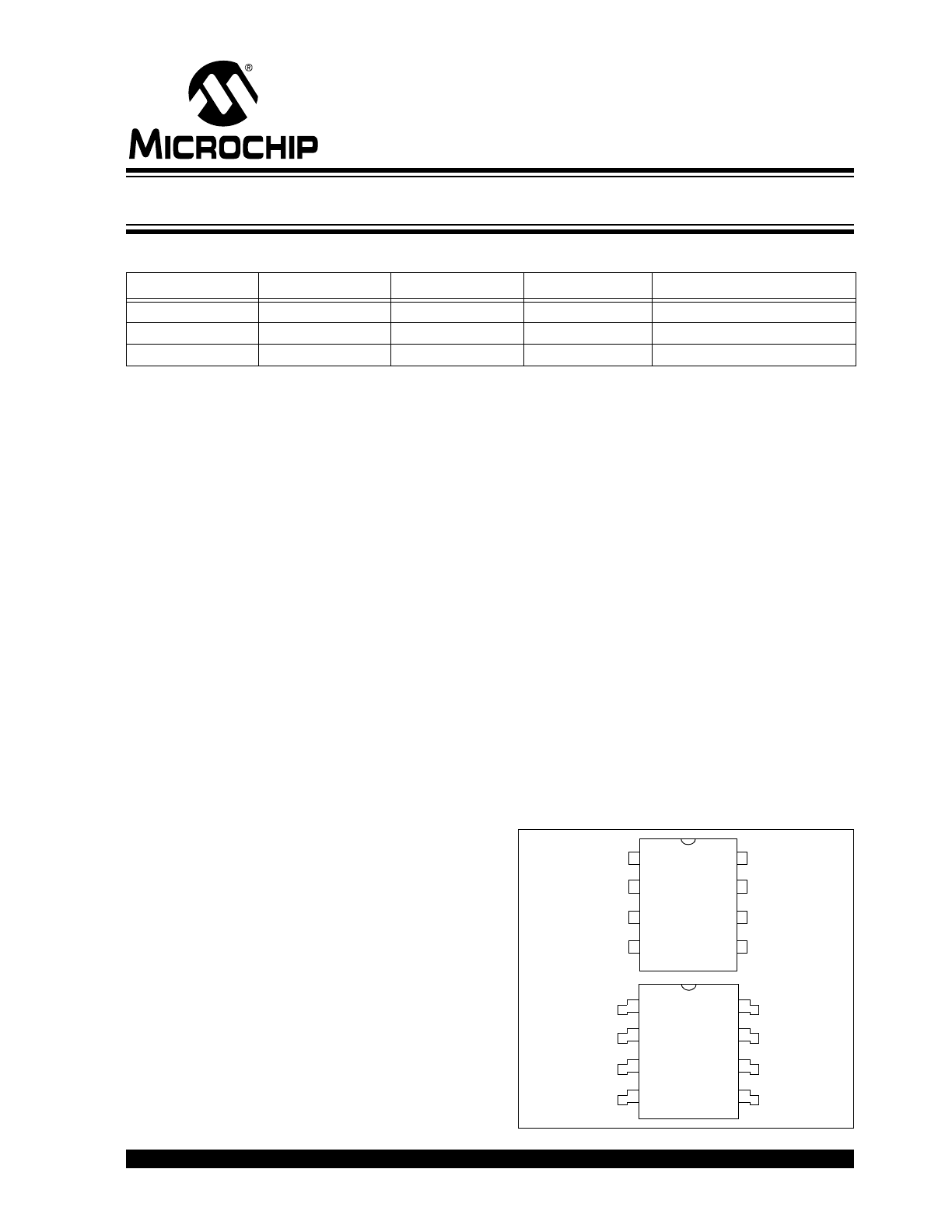
applications. The 24XX65 is available in the standard
8-pin plastic DIP and 8-pin surface mount SOIJ
package.
Package Types
Part Number
V
CC
Range
Page Size
Temp. Ranges
Packages
24AA65
1.8-6.0V
64 Bytes
C
P, SM
24LC65
2.5-6.0V
64 Bytes
C, I
P, SM
24C65
4.5-6.0V
64 Bytes
C, I, E
P, SM
- Industrial (I)
-40°C to
+85°C
- Automotive (E)
-40°C to +125°C
24
XX65
A0
A1
A2
V
SS
1
2
3
4
8
7
6
5
V
CC
NC
SCL
SDA
24XX6
5
A0
A1
A2
V
SS
1
2
3
4
8
7
6
5
V
CC
NC
SCL
SDA
PDIP
SOIJ
64K I
2
C
™
Smart Serial
™
EEPROM
*24XX65 is used in this document as a generic part
number for the 24AA65/24LC65/24C65 devices.
24AA65/24LC65/24C65
DS21073K-page 2
© 2008 Microchip Technology Inc.
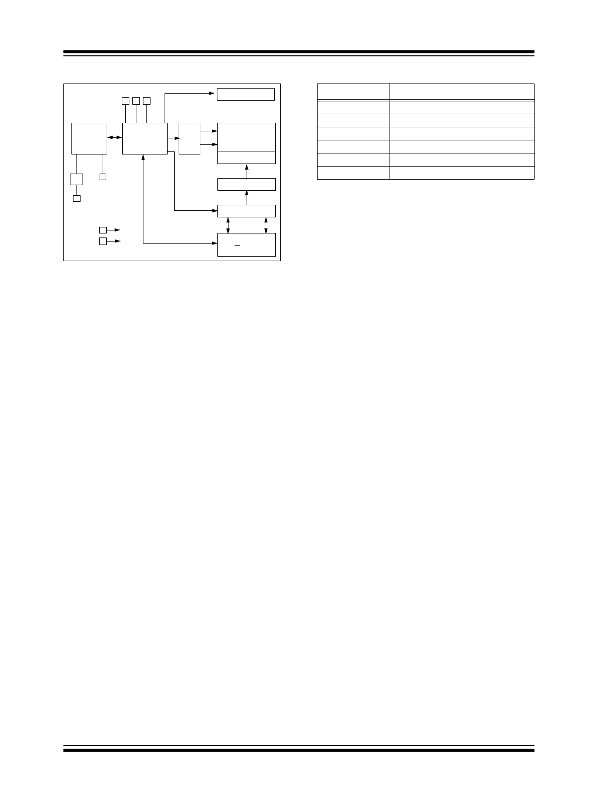
Block Diagram
Pin Function Table
HV Generator
EEPROM
Array
Page Latches
YDEC
XDEC
Sense
Amp.
R/W Control
Memory
Control
Logic
I/O
Control
Logic
SDA
SCL
V
CC
V
SS
I/O
A2
A1
A0
Cache
Name
Function
A0, A1, A2
User Configurable Chip Selects
V
SS
Ground
SDA
Serial Address/Data/I/O
SCL
Serial Clock
V
CC
+1.8V to 6.0V Power Supply
NC
No Internal Connection
© 2008 Microchip Technology Inc.
DS21073K-page 3
24AA65/24LC65/24C65
1.0
ELECTRICAL CHARACTERISTICS
Absolute Maximum Ratings
(†)
V
CC
............................................................................................................................................................................. 7.0V
All inputs and outputs w.r.t. V
SS
..........................................................................................................-0.6V to V
CC
+1.0V
Storage temperature ............................................................................................................................... -65°C to +150°C
Ambient temperature with power applied................................................................................................-40°C to +125°C
ESD protection on all pins
......................................................................................................................................................≥ 4 kV
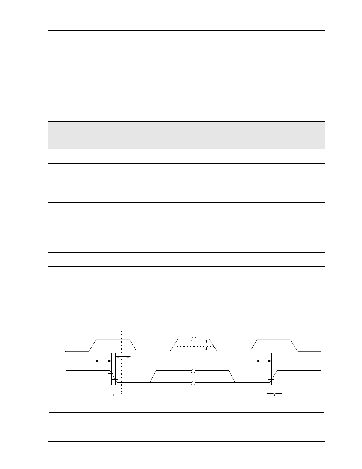
TABLE 1-1:
DC CHARACTERISTICS
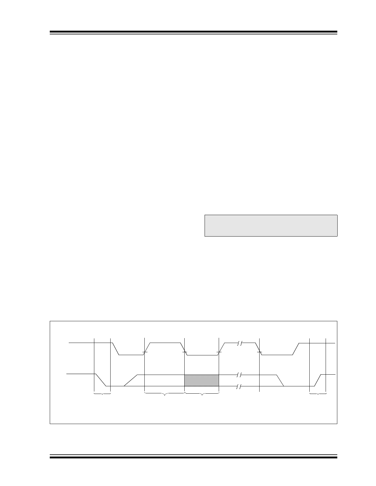
FIGURE 1-1:
BUS TIMING START/STOP
† NOTICE: Stresses above those listed under “Absolute Maximum Ratings” may cause permanent damage to the
device. This is a stress rating only and functional operation of the device at those or any other conditions above those
indicated in the operational listings of this specification is not implied. Exposure to maximum rating conditions for an
extended period of time may affect device reliability.
DC CHARACTERISTICS
V
CC
= +1.8V to +6.0V
Commercial (C): T
A
=
0
°C to +70°C
Industrial
(I): T
A
=
-40
°C to +85°C
Automotive
(E): T
A
=
-40
°C to +125°C
Parameter
Sym
Min
Max
Units
Conditions
A0, A1, A2, SCL and SDA pins:
High-level input voltage
Low-level input voltage
Hysteresis of Schmitt Trigger inputs
Low-level output voltage
V
IH
V
IL
V
HYS
V
OL
.7 V
CC
—
.05 V
CC
—
—
.3 V
CC
—
.40
V
V
V
V
(Note 1)
I
OL
= 3.0 mA
Input leakage current
I
LI
—
±1
μA
V
IN
= .1V to V
CC
Output leakage current
I
LO
—
±1
μA
V
OUT
= .1V to V
CC
Pin capacitance
(all inputs/outputs)
C
IN
, C
OUT
—
10
pF
V
CC
= 5.0V (Note 1)
T
A
= 25°C, F
CLK
= 1 MHz
Operating current
I
CC
Write
I
CC
Read
—
—
3
150
mA
μA
V
CC
= 6.0V, SCL = 400 kHz
V
CC
= 6.0V, SCL = 400 kHz
Standby current
I
CCS
—
5
μA
V
CC
= 5.0V, SCL = SDA = V
CC
A0, A1, A2 = V
SS
Note 1:
This parameter is periodically sampled and not 100% tested.
T
SU
:
STA
T
HD
:
STA
V
HYS
T
SU
:
STO
Start
Stop
SCL
SDA
24AA65/24LC65/24C65
DS21073K-page 4
© 2008 Microchip Technology Inc.
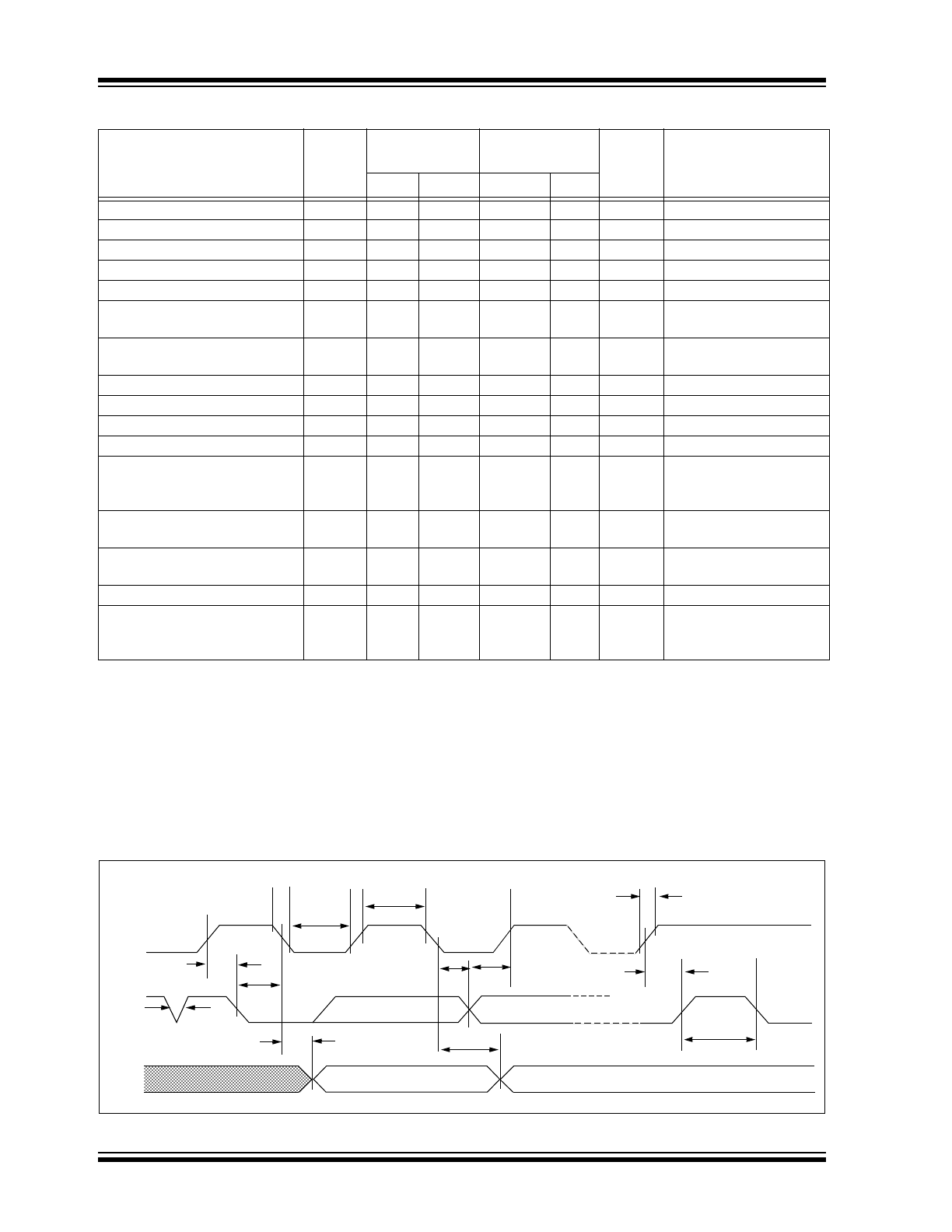
TABLE 1-2:
AC CHARACTERISTICS
FIGURE 1-2:
BUS TIMING DATA
Parameter
Symbol
V
CC
= 1.8V-6.0V
STD. Mode
V
CC
= 4.5-6.0V
FAST Mode
Units
Remarks
Min
Max
Min
Max
Clock frequency
F
CLK
—
100
—
400
kHz
Clock high time
T
HIGH
4000
—
600
—
ns
Clock low time
T
LOW
4700
—
1300
—
ns
SDA and SCL rise time
T
R
—
1000
—
300
ns
(Note 1)
SDA and SCL fall time
T
F
—
300
—
300
ns
(Note 1)
Start condition setup time
T
HD
:
STA
4000
—
600
—
ns
After this period the first
clock pulse is generated
Start condition setup time
T
SU
:
STA
4700
—
600
—
ns
Only relevant for
repeated Start condition
Data input hold time
T
HD
:
DAT
0
—
0
—
ns
Data input setup time
T
SU
:
DAT
250
—
100
—
ns
Stop condition setup time
T
SU
:
STO
4000
—
600
—
ns
Output valid from clock
T
AA
—
3500
—
900
ns
(Note 2)
Bus free time
T
BUF
4700
—
1300
—
ns
Time the bus must be
free before a new
transmission can start
Output fall time from V
IH
min to
V
IL
max
T
OF
—
250
20 + 0.1
C
B
250
ns
(Note 1), C
B
≤ 100 pF
Input filter spike suppression
(SDA and SCL pins)
T
SP
50
—
50
—
ns
(Note 3)
Write cycle time
T
WR
—
5
—
5
ms/page (Note 4)
Endurance
High Endurance Block
Rest of Array
10M
1M
—
—
10M
1M
—
—
cycles
25°C, (Note 5)
Note 1:
Not 100 percent tested. C
B
= total capacitance of one bus line in pF.
2:
As a transmitter, the device must provide an internal minimum delay time to bridge the undefined region
(minimum 300 ns) of the falling edge of SCL to avoid unintended generation of Start or Stop conditions.
3:
The combined T
SP
and V
HYS
specifications are due to new Schmitt Trigger inputs which provide improved
noise and spike suppression. This eliminates the need for a Ti specification for standard operation.
4:
The times shown are for a single page of 8 bytes. Multiply by the number of pages loaded into the write
cache for total time.
5:
This parameter is not tested but ensured by characterization. For endurance estimates in a specific
application, please consult the Total Endurance™ Model which can be downloaded at www.microchip.com.
SCL
SDA
IN
SDA
OUT
T
SU
:
STA
T
SP
T
AA
T
F
T
LOW
T
HIGH
T
HD
:
STA
T
HD
:
DAT
T
SU
:
DAT
T
SU
:
STO
T
BUF
T
AA
T
R
© 2008 Microchip Technology Inc.
DS21073K-page 5
24AA65/24LC65/24C65
2.0
FUNCTIONAL DESCRIPTION
The 24XX65 supports a bidirectional two-wire bus and
data transmission protocol. A device that sends data
onto the bus is defined as transmitter, and a device
receiving data as receiver. The bus must be controlled
by a master device which generates the serial clock
(SCL), controls the bus access and generates the Start
and Stop conditions, while the 24XX65 works as slave.
Both master and slave can operate as transmitter or
receiver, but the master device determines which mode
is activated.
3.0
BUS CHARACTERISTICS
The following bus protocol has been defined:
• Data transfer may be initiated only when the bus
is not busy.
• During data transfer, the data line must remain
stable whenever the clock line is high. Changes in
the data line while the clock line is high will be
interpreted as a Start or Stop condition.
Accordingly, the following bus conditions have been
defined (Figure 3-1).
3.1
Bus not Busy (A)
Both data and clock lines remain high.
3.2
Start Data Transfer (B)
A high-to-low transition of the SDA line while the clock
(SCL) is high determines a Start condition. All
commands must be preceded by a Start condition.
3.3
Stop Data Transfer (C)
A low-to-high transition of the SDA line while the clock
(SCL) is high determines a Stop condition. All
operations must be ended with a Stop condition.
3.4
Data Valid (D)
The state of the data line represents valid data when,
after a Start condition, the data line is stable for the
duration of the high period of the clock signal.
The data on the line must be changed during the low
period of the clock signal. There is one clock pulse per
bit of data.
Each data transfer is initiated with a Start condition and
terminated with a Stop condition. The number of the
data bytes transferred between the Start and Stop
conditions is determined by the master device.
3.5
Acknowledge
Each receiving device, when addressed, is obliged to
generate an acknowledge after the reception of each
byte. The master device must generate an extra clock
pulse which is associated with this Acknowledge bit.
A device that acknowledges must pull down the SDA
line during the Acknowledge clock pulse in such a way
that the SDA line is stable low during the high period of
the acknowledge related clock pulse. Of course, setup
and hold times must be taken into account. During
reads, a master must signal an end of data to the slave
by NOT generating an Acknowledge bit on the last byte
that has been clocked out of the slave. In this case, the
slave (24XX65) must leave the data line high to enable
the master to generate the Stop condition.
FIGURE 3-1:
DATA TRANSFER SEQUENCE ON THE SERIAL BUS
Note:
The 24XX65 does not generate any
Acknowledge bits if an internal program-
ming cycle is in progress.
SCL
SDA
(A)
(B)
(D)
(D)
(A)
(C)
Start
Condition
Address or
Acknowledge
Valid
Data
Allowed
To Change
Stop
Condition
24AA65/24LC65/24C65
DS21073K-page 6
© 2008 Microchip Technology Inc.
3.6
Device Addressing
A control byte is the first byte received following the
Start condition from the master device. The control byte
consists of a four-bit control code, for the 24XX65 this
is set as ‘1010’ binary for read and write operations.
The next three bits of the control byte are the device
select bits (A2, A1, A0). They are used by the master
device to select which of the eight devices are to be
accessed. These bits are in effect the three Most
Significant bits of the word address. The last bit of the
control byte defines the operation to be performed.
When set to a one a read operation is selected, when
set to a zero a write operation is selected. The next two
bytes received define the address of the first data byte
(Figure 4-1). Because only A12..A0 are used, the
upper three address bits must be zeros. The Most
Significant bit of the Most Significant Byte is transferred
first. Following the Start condition, the 24XX65
monitors the SDA bus checking the device type
identifier being transmitted. Upon receiving a ‘1010’
code and appropriate device select bits, the slave
device (24XX65) outputs an Acknowledge signal on the
SDA line. Depending upon the state of the R/W bit, the
24XX65 will select a read or write operation.
FIGURE 3-2:
CONTROL BYTE
ALLOCATION
4.0
WRITE OPERATION
4.1
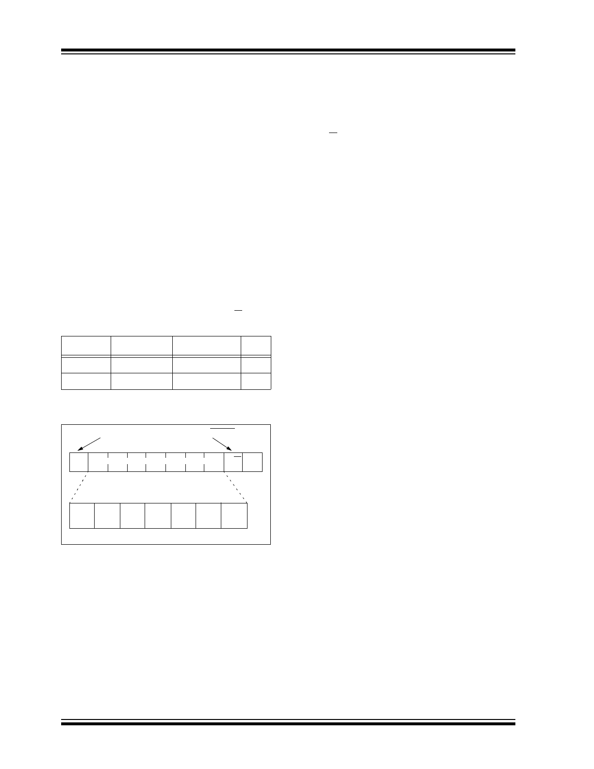
Byte Write
Following the Start condition from the master, the con-
trol code (four bits), the device select (three bits), and
the R/W bit which is a logic low, is placed onto the bus
by the master transmitter. This indicates to the
addressed slave receiver (24XX65) that a byte with a
word address will follow after it has generated an
Acknowledge bit during the ninth clock cycle. There-
fore, the next byte transmitted by the master is the
high-order byte of the word address and will be written
into the Address Pointer of the 24XX65. The next byte
is the Least Significant Address Byte. After receiving
another Acknowledge signal from the 24XX65, the
master device will transmit the data word to be written
into the addressed memory location. The 24XX65
acknowledges again and the master generates a Stop
condition. This initiates the internal write cycle, and
during this time the 24XX65 will not generate
Acknowledge signals (Figure 4-1).
4.2
Page Write
The write control byte, word address and the first data
byte are transmitted to the 24XX65 in the same way as
in a byte write. But instead of generating a Stop
condition, the master transmits up to eight pages of
eight data bytes each (64 bytes total), which are
temporarily stored in the on-chip page cache of the
24XX65. They will be written from the cache into the
EEPROM array after the master has transmitted a Stop
condition. After the receipt of each word, the six lower
order Address Pointer bits are internally incremented by
one. The higher order seven bits of the word address
remain constant. If the master should transmit more
than eight bytes prior to generating the Stop condition
(writing across a page boundary), the address counter
(lower three bits) will roll over and the pointer will be
incremented to point to the next line in the cache. This
can continue to occur up to eight times or until the cache
is full, at which time a Stop condition should be
generated by the master. If a Stop condition is not
received, the cache pointer will roll over to the first line
(byte 0) of the cache, and any further data received will
overwrite previously captured data. The Stop condition
can be sent at any time during the transfer. As with the
byte write operation, once the Stop condition is received
an internal write cycle will begin. The 64-byte cache will
continue to capture data until a Stop condition occurs or
the operation is aborted (Figure 4-2).
Operation Control Code
Device Select
R/W
Read
1010
Device Address
1
Write
1010
Device Address
0
SLAVE ADDRESS
1
0
1
0
A2
A1
A0
R/W
A
START
READ/WRITE
© 2008 Microchip Technology Inc.
DS21073K-page 7
24AA65/24LC65/24C65
FIGURE 4-1:
BYTE WRITE
FIGURE 4-2:
PAGE WRITE (FOR CACHE WRITE, SEE FIGURE 8-2)
FIGURE 4-3:
CURRENT ADDRESS READ
0 0 0
Bus Activity
Master
SDA Line
Bus Activity
S
T
A
R
T
Control
Byte
Word
Address (1)
Word
Address (0)
Data
A
C
K
A
C
K
A
C
K
A
C
K
S
T
O
P
S
P
Bus
Master
SDA Line
Bus
Control
Byte
Word
Address
(1)
S
T
O
P
S
T
A
R
T
A
C
K
0
A
C
K
A
C
K
Activity
Activity
:
A
C
K
A
C
K
Data n
Data n + 7
0 0
Word
Address
(0)
P
S
S
P
Bus Activity
Master
SDA Line
Bus Activity
S
T
A
R
T
S
T
O
P
Control
Byte
Data n
A
C
K
N
O
A
C
K
24AA65/24LC65/24C65
DS21073K-page 8
© 2008 Microchip Technology Inc.
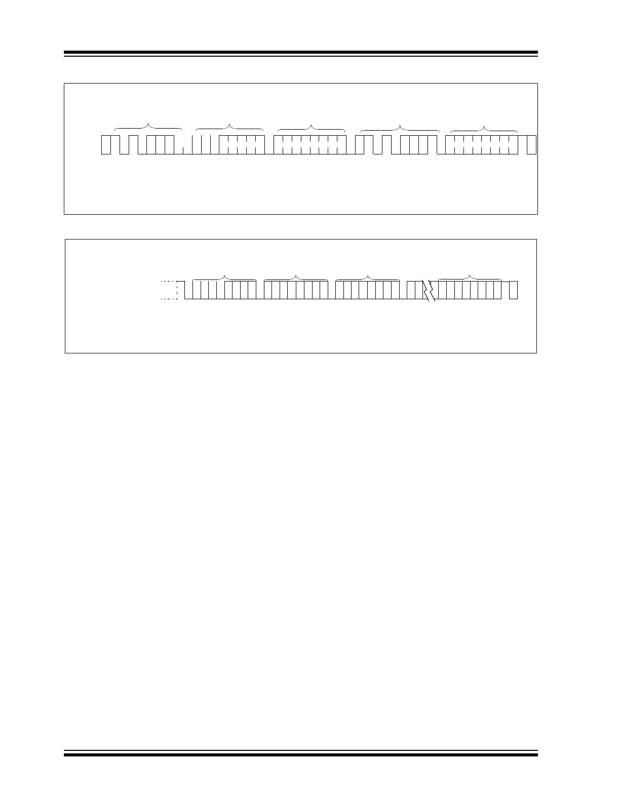
FIGURE 4-4:
RANDOM READ
FIGURE 4-5:
SEQUENTIAL READ
SDA Line
Bus
Control
Byte
Word
Address (1)
S
T
O
P
S
T
A
R
T
A
C
K
A
C
K
A
C
K
Activity
A
C
K
N
O
Data n
0 0 0
Word
Address (0)
S
T
A
R
T
Control
Byte
A
C
K
P
S
S
P
Bus Activity
Master
SDA Line
Bus Activity
S
T
O
P
Control
Byte
A
C
K
N
O
A
C
K
Data n
Data n + 1
Data n + 2
Data n + X
A
C
K
A
C
K
A
C
K

© 2008 Microchip Technology Inc.
DS21073K-page 9
24AA65/24LC65/24C65
5.0
READ OPERATION
Read operations are initiated in the same way as write
operations with the exception that the R/W bit of the
slave address is set to one. There are three basic types
of read operations: current address read, random read
and sequential read.
5.1
Current Address Read
The 24XX65 contains an address counter that main-
tains the address of the last word accessed, internally
incremented by one. Therefore, if the previous access
(either a read or write operation) was to address n (n is
any legal address), the next current address read
operation would access data from address n + 1. Upon
receipt of the slave address with R/W bit set to one, the
24XX65 issues an acknowledge and transmits the
eight-bit data word. The master will not acknowledge
the transfer but does generate a Stop condition and the
24XX65 discontinues transmission (Figure 4-3).
5.2
Random Read
Random read operations allow the master to access
any memory location in a random manner. To perform
this type of read operation, first the word address must
be set. This is done by sending the word address to the
24XX65 as part of a write operation (R/W bit set to ‘0’).
After the word address is sent, the master generates a
Start condition following the acknowledge. This
terminates the write operation, but not before the
internal Address Pointer is set. Then the master issues
the control byte again, but with the R/W bit set to a one.
The 24XX65 will then issue an acknowledge and
transmit the eight-bit data word. The master will not
acknowledge the transfer, but does generate a Stop
condition which causes the 24XX65 to discontinue
transmission (Figure 4-4).
5.3
Sequential Read
Sequential reads are initiated in the same way as a
random read except that after the 24XX65 transmits the
first data byte, the master issues an acknowledge as
opposed to the Stop condition used in a random read.
This acknowledge directs the 24XX65 to transmit the
next sequentially addressed 8-bit word (Figure 4-5).
Following the final byte transmitted to the master, the
master will NOT generate an acknowledge, but will
generate a Stop condition.
To provide sequential reads the 24XX65 contains an
internal Address Pointer which is incremented by one
at the completion of each operation. This Address
Pointer allows the entire memory contents to be serially
read during one operation.
5.4
Contiguous Addressing Across
Multiple Devices
The device select bits A2, A1, A0 can be used to
expand the contiguous address space for up to 512K
bits by adding up to eight 24XX65's on the same bus.
In this case, software can use A0 of the control byte as
address bit A13, A1 as address bit A14 and A2 as
address bit A15.
5.5
Noise Protection
The SCL and SDA inputs have filter circuits which
suppress noise spikes to assure proper device
operation even on a noisy bus. All I/O lines incorporate
Schmitt Triggers for 400 kHz (Fast mode) compatibility.
5.6
High Endurance Block
The location of the high endurance block within the
memory map is programmed by setting the leading bit
7 (S/HE) of the configuration byte to ‘0’. The upper bits
of the address loaded in this command will determine
which 4K block within the memory map will be set to
high endurance. This block will be capable of
10,000,000 erase/write cycles typical (Figure 8-1).
The high endurance block will retain its value as the
high endurance block even if it resides within the
security block range. The high endurance setting
always takes precedence to the security setting.
Note:
The high endurance block cannot be
changed after the security option has been
set with a length greater than zero. If the
H.E. block is not programmed by the user,
the default location is the highest block of
memory which starts at location 0x1E00
and ends at 0x1FFF.
24AA65/24LC65/24C65
DS21073K-page 10
© 2008 Microchip Technology Inc.
5.7
Security Options
The 24XX65 has a sophisticated mechanism for write
protecting portions of the array. This write-protect
function is programmable and allows the user to protect
0-15 contiguous 4K blocks. The user sets the security
option by sending to the device the starting block
number for the protected region and the number of
blocks to be protected. All parts will come from the
factory in the default configuration with the starting
block number set to 15 and the number of protected
blocks set to zero. THE SECURITY OPTION CAN BE
SET ONLY ONCE WITH A LENGTH GREATER THAN
ZERO.
To invoke the security option, a Write command is sent
to the device with the leading bit (bit 7) of the first
address byte set to a ‘1’ (Figure 8-1). Bits 1-4 of the first
address byte define the starting block number for the
protected region.
For example, if the starting block number is to be set to
5, the first address byte would be 1XX0101X. Bits 0, 5
and 6 of the first address byte are disregarded by the
device and can be either high or low. The device will
acknowledge after the first address byte. A byte of
“don’t care” bits is then sent by the master, with the
device acknowledging afterwards. The third byte sent
to the device has bit 7 (S/HE) set high and bit 6 (R) set
low. Bits 4 and 5 are “don’t cares” and bits 0-3 define
the number of blocks to be write-protected. For exam-
ple, if three blocks are to be protected, the third byte
would be 10XX0011. After the third byte is sent to the
device, it will acknowledge and a Stop bit is then sent
by the master to complete the command.
If one of the security blocks coincides with the high
endurance block, the high endurance setting will take
precedence. Also, if the range of the security blocks
encompass the high endurance block when the secu-
rity option is set, the security block range will be set
accordingly, but the high endurance block will continue
to retain the high endurance setting. As a result, the
memory blocks preceding the high endurance block will
be set as secure sections.
During a normal write sequence, if an attempt is made
to write to a protected address, no data will be written
and the device will not report an error or abort the
command. If a Write command is attempted across a
secure boundary, unprotected addresses will be written
and protected addresses will not.
5.8
Security Configuration Read
The status of the secure portion of memory can be read
by using the same technique as programming this
option except the read bit (bit 6) of the configuration
byte is set to a one. After the configuration byte is sent,
the device will acknowledge and then send two bytes of
data to the master just as in a normal read sequence.
The master must acknowledge the first byte and not
acknowledge the second, and then send a Stop bit to
end the sequence. The upper four bits of both of these
bytes will always be read as ‘1’s. The lower four bits of
the first byte contains the starting secure block. The
lower four bits of the second byte contains the number
of secure blocks. The default starting secure block is
fifteen and the default number of secure blocks is zero
(Figure 8-1).
6.0
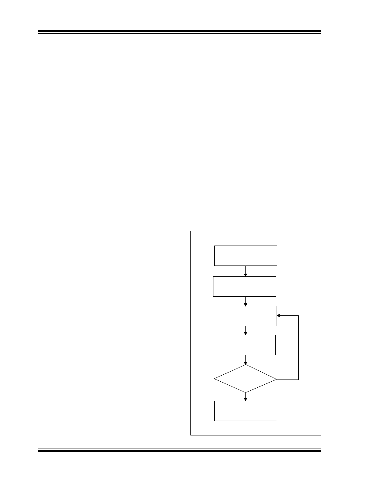
ACKNOWLEDGE POLLING
Since the device will not acknowledge during a write
cycle, this can be used to determine when the cycle is
complete (this feature can be used to maximize bus
throughput). Once the Stop condition for a Write
command has been issued from the master, the device
initiates the internally timed write cycle. ACK polling
can be initiated immediately. This involves the master
sending a Start condition followed by the control byte
for a Write command (R/W = 0). If the device is still
busy with the write cycle, then no ACK will be returned.
If the cycle is complete, then the device will return the
ACK and the master can then proceed with the next
Read or Write command. See Figure 6-1 for flow
diagram.
FIGURE 6-1:
ACKNOWLEDGE
POLLING FLOW
Send
Write Command
Send Stop
Condition to
Initiate Write Cycle
Send Start
Send Control Byte
with R/W = 0
Did Device
Acknowledge
(ACK = 0)?
Next
Operation
NO
YES
© 2008 Microchip Technology Inc.
DS21073K-page 1
24AA65/24LC65/24C65
Device Selection Table
Features:
• Voltage Operating Range: 1.8V to 6.0V
- Peak write current 3 mA at 6.0V
- Maximum read current 150
μA at 6.0V
- Standby current 1
μA, typical
• Industry Standard Two-Wire Bus Protocol I
2
C™
Compatible
• 8-Byte Page, or Byte modes Available
• 2 ms Typical Write Cycle Time, Byte or Page
• 64-Byte Input Cache for Fast Write Loads
• Up to 8 devices may be connected to the same
bus for up to 512K bits total memory
• Including 100 kHz (1.8V
≤ Vcc < 4.5V) and 400
kHz (4.5V
≤ V
CC
≤ 6.0V) Compatibility
• Programmable Block Security Options
• Programmable Endurance Options
• Schmitt Trigger, Filtered Inputs for Noise
Suppression
• Output Slope Control to Eliminate Ground Bounce
• Self-Timed Erase and Write Cycles
• Power-on/off Data Protection Circuitry
• Endurance:
- 10,000,000 E/W cycles for a High Endurance
Block
- 1,000,000 E/W cycles for a Standard
Endurance Block
• Electrostatic Discharge Protection > 4000V
• Data Retention > 200 years
• 8-pin PDIP/SOIJ Packages
• Temperature Ranges
• Pb-Free and RoHS Compliant
Description:
The Microchip Technology Inc. 24AA65/24LC65/
24C65 (24XX65)* is a “smart” 8K x 8 Serial Electrically
Erasable PROM. This device has been developed for
advanced, low-power applications such as personal
communications, and provides the systems designer
with flexibility through the use of many new user-pro-
grammable features. The 24XX65 offers a relocatable
4K bit block of ultra-high-endurance memory for data
that changes frequently. The remainder of the array, or
60K bits, is rated at 1,000,000 erase/write (E/W) cycles
ensured. The 24XX65 features an input cache for fast
write loads with a capacity of eight pages, or 64 bytes.
This device also features programmable security
options for E/W protection of critical data and/or code
of up to fifteen 4K blocks. Functional address lines
allow the connection of up to eight 24XX65’s on the
same bus for up to 512K bits contiguous EEPROM
memory. Advanced CMOS technology makes this
device ideal for low-power nonvolatile code and data
applications. The 24XX65 is available in the standard
8-pin plastic DIP and 8-pin surface mount SOIJ
package.
Package Types
Part Number
V
CC
Range
Page Size
Temp. Ranges
Packages
24AA65
1.8-6.0V
64 Bytes
C
P, SM
24LC65
2.5-6.0V
64 Bytes
C, I
P, SM
24C65
4.5-6.0V
64 Bytes
C, I, E
P, SM
- Industrial (I)
-40°C to
+85°C
- Automotive (E)
-40°C to +125°C
24
XX65
A0
A1
A2
V
SS
1
2
3
4
8
7
6
5
V
CC
NC
SCL
SDA
24XX6
5
A0
A1
A2
V
SS
1
2
3
4
8
7
6
5
V
CC
NC
SCL
SDA
PDIP
SOIJ
64K I
2
C
™
Smart Serial
™
EEPROM
*24XX65 is used in this document as a generic part
number for the 24AA65/24LC65/24C65 devices.
24AA65/24LC65/24C65
DS21073K-page 2
© 2008 Microchip Technology Inc.
Block Diagram
Pin Function Table
HV Generator
EEPROM
Array
Page Latches
YDEC
XDEC
Sense
Amp.
R/W Control
Memory
Control
Logic
I/O
Control
Logic
SDA
SCL
V
CC
V
SS
I/O
A2
A1
A0
Cache
Name
Function
A0, A1, A2
User Configurable Chip Selects
V
SS
Ground
SDA
Serial Address/Data/I/O
SCL
Serial Clock
V
CC
+1.8V to 6.0V Power Supply
NC
No Internal Connection
© 2008 Microchip Technology Inc.
DS21073K-page 3
24AA65/24LC65/24C65
1.0
ELECTRICAL CHARACTERISTICS
Absolute Maximum Ratings
(†)
V
CC
............................................................................................................................................................................. 7.0V
All inputs and outputs w.r.t. V
SS
..........................................................................................................-0.6V to V
CC
+1.0V
Storage temperature ............................................................................................................................... -65°C to +150°C
Ambient temperature with power applied................................................................................................-40°C to +125°C
ESD protection on all pins
......................................................................................................................................................≥ 4 kV
TABLE 1-1:
DC CHARACTERISTICS
FIGURE 1-1:
BUS TIMING START/STOP
† NOTICE: Stresses above those listed under “Absolute Maximum Ratings” may cause permanent damage to the
device. This is a stress rating only and functional operation of the device at those or any other conditions above those
indicated in the operational listings of this specification is not implied. Exposure to maximum rating conditions for an
extended period of time may affect device reliability.
DC CHARACTERISTICS
V
CC
= +1.8V to +6.0V
Commercial (C): T
A
=
0
°C to +70°C
Industrial
(I): T
A
=
-40
°C to +85°C
Automotive
(E): T
A
=
-40
°C to +125°C
Parameter
Sym
Min
Max
Units
Conditions
A0, A1, A2, SCL and SDA pins:
High-level input voltage
Low-level input voltage
Hysteresis of Schmitt Trigger inputs
Low-level output voltage
V
IH
V
IL
V
HYS
V
OL
.7 V
CC
—
.05 V
CC
—
—
.3 V
CC
—
.40
V
V
V
V
(Note 1)
I
OL
= 3.0 mA
Input leakage current
I
LI
—
±1
μA
V
IN
= .1V to V
CC
Output leakage current
I
LO
—
±1
μA
V
OUT
= .1V to V
CC
Pin capacitance
(all inputs/outputs)
C
IN
, C
OUT
—
10
pF
V
CC
= 5.0V (Note 1)
T
A
= 25°C, F
CLK
= 1 MHz
Operating current
I
CC
Write
I
CC
Read
—
—
3
150
mA
μA
V
CC
= 6.0V, SCL = 400 kHz
V
CC
= 6.0V, SCL = 400 kHz
Standby current
I
CCS
—
5
μA
V
CC
= 5.0V, SCL = SDA = V
CC
A0, A1, A2 = V
SS
Note 1:
This parameter is periodically sampled and not 100% tested.
T
SU
:
STA
T
HD
:
STA
V
HYS
T
SU
:
STO
Start
Stop
SCL
SDA
24AA65/24LC65/24C65
DS21073K-page 4
© 2008 Microchip Technology Inc.
TABLE 1-2:
AC CHARACTERISTICS
FIGURE 1-2:
BUS TIMING DATA
Parameter
Symbol
V
CC
= 1.8V-6.0V
STD. Mode
V
CC
= 4.5-6.0V
FAST Mode
Units
Remarks
Min
Max
Min
Max
Clock frequency
F
CLK
—
100
—
400
kHz
Clock high time
T
HIGH
4000
—
600
—
ns
Clock low time
T
LOW
4700
—
1300
—
ns
SDA and SCL rise time
T
R
—
1000
—
300
ns
(Note 1)
SDA and SCL fall time
T
F
—
300
—
300
ns
(Note 1)
Start condition setup time
T
HD
:
STA
4000
—
600
—
ns
After this period the first
clock pulse is generated
Start condition setup time
T
SU
:
STA
4700
—
600
—
ns
Only relevant for
repeated Start condition
Data input hold time
T
HD
:
DAT
0
—
0
—
ns
Data input setup time
T
SU
:
DAT
250
—
100
—
ns
Stop condition setup time
T
SU
:
STO
4000
—
600
—
ns
Output valid from clock
T
AA
—
3500
—
900
ns
(Note 2)
Bus free time
T
BUF
4700
—
1300
—
ns
Time the bus must be
free before a new
transmission can start
Output fall time from V
IH
min to
V
IL
max
T
OF
—
250
20 + 0.1
C
B
250
ns
(Note 1), C
B
≤ 100 pF
Input filter spike suppression
(SDA and SCL pins)
T
SP
50
—
50
—
ns
(Note 3)
Write cycle time
T
WR
—
5
—
5
ms/page (Note 4)
Endurance
High Endurance Block
Rest of Array
10M
1M
—
—
10M
1M
—
—
cycles
25°C, (Note 5)
Note 1:
Not 100 percent tested. C
B
= total capacitance of one bus line in pF.
2:
As a transmitter, the device must provide an internal minimum delay time to bridge the undefined region
(minimum 300 ns) of the falling edge of SCL to avoid unintended generation of Start or Stop conditions.
3:
The combined T
SP
and V
HYS
specifications are due to new Schmitt Trigger inputs which provide improved
noise and spike suppression. This eliminates the need for a Ti specification for standard operation.
4:
The times shown are for a single page of 8 bytes. Multiply by the number of pages loaded into the write
cache for total time.
5:
This parameter is not tested but ensured by characterization. For endurance estimates in a specific
application, please consult the Total Endurance™ Model which can be downloaded at www.microchip.com.
SCL
SDA
IN
SDA
OUT
T
SU
:
STA
T
SP
T
AA
T
F
T
LOW
T
HIGH
T
HD
:
STA
T
HD
:
DAT
T
SU
:
DAT
T
SU
:
STO
T
BUF
T
AA
T
R
© 2008 Microchip Technology Inc.
DS21073K-page 5
24AA65/24LC65/24C65
2.0
FUNCTIONAL DESCRIPTION
The 24XX65 supports a bidirectional two-wire bus and
data transmission protocol. A device that sends data
onto the bus is defined as transmitter, and a device
receiving data as receiver. The bus must be controlled
by a master device which generates the serial clock
(SCL), controls the bus access and generates the Start
and Stop conditions, while the 24XX65 works as slave.
Both master and slave can operate as transmitter or
receiver, but the master device determines which mode
is activated.
3.0
BUS CHARACTERISTICS
The following bus protocol has been defined:
• Data transfer may be initiated only when the bus
is not busy.
• During data transfer, the data line must remain
stable whenever the clock line is high. Changes in
the data line while the clock line is high will be
interpreted as a Start or Stop condition.
Accordingly, the following bus conditions have been
defined (Figure 3-1).
3.1
Bus not Busy (A)
Both data and clock lines remain high.
3.2
Start Data Transfer (B)
A high-to-low transition of the SDA line while the clock
(SCL) is high determines a Start condition. All
commands must be preceded by a Start condition.
3.3
Stop Data Transfer (C)
A low-to-high transition of the SDA line while the clock
(SCL) is high determines a Stop condition. All
operations must be ended with a Stop condition.
3.4
Data Valid (D)
The state of the data line represents valid data when,
after a Start condition, the data line is stable for the
duration of the high period of the clock signal.
The data on the line must be changed during the low
period of the clock signal. There is one clock pulse per
bit of data.
Each data transfer is initiated with a Start condition and
terminated with a Stop condition. The number of the
data bytes transferred between the Start and Stop
conditions is determined by the master device.
3.5
Acknowledge
Each receiving device, when addressed, is obliged to
generate an acknowledge after the reception of each
byte. The master device must generate an extra clock
pulse which is associated with this Acknowledge bit.
A device that acknowledges must pull down the SDA
line during the Acknowledge clock pulse in such a way
that the SDA line is stable low during the high period of
the acknowledge related clock pulse. Of course, setup
and hold times must be taken into account. During
reads, a master must signal an end of data to the slave
by NOT generating an Acknowledge bit on the last byte
that has been clocked out of the slave. In this case, the
slave (24XX65) must leave the data line high to enable
the master to generate the Stop condition.
FIGURE 3-1:
DATA TRANSFER SEQUENCE ON THE SERIAL BUS
Note:
The 24XX65 does not generate any
Acknowledge bits if an internal program-
ming cycle is in progress.
SCL
SDA
(A)
(B)
(D)
(D)
(A)
(C)
Start
Condition
Address or
Acknowledge
Valid
Data
Allowed
To Change
Stop
Condition
24AA65/24LC65/24C65
DS21073K-page 6
© 2008 Microchip Technology Inc.
3.6
Device Addressing
A control byte is the first byte received following the
Start condition from the master device. The control byte
consists of a four-bit control code, for the 24XX65 this
is set as ‘1010’ binary for read and write operations.
The next three bits of the control byte are the device
select bits (A2, A1, A0). They are used by the master
device to select which of the eight devices are to be
accessed. These bits are in effect the three Most
Significant bits of the word address. The last bit of the
control byte defines the operation to be performed.
When set to a one a read operation is selected, when
set to a zero a write operation is selected. The next two
bytes received define the address of the first data byte
(Figure 4-1). Because only A12..A0 are used, the
upper three address bits must be zeros. The Most
Significant bit of the Most Significant Byte is transferred
first. Following the Start condition, the 24XX65
monitors the SDA bus checking the device type
identifier being transmitted. Upon receiving a ‘1010’
code and appropriate device select bits, the slave
device (24XX65) outputs an Acknowledge signal on the
SDA line. Depending upon the state of the R/W bit, the
24XX65 will select a read or write operation.
FIGURE 3-2:
CONTROL BYTE
ALLOCATION
4.0
WRITE OPERATION
4.1
Byte Write
Following the Start condition from the master, the con-
trol code (four bits), the device select (three bits), and
the R/W bit which is a logic low, is placed onto the bus
by the master transmitter. This indicates to the
addressed slave receiver (24XX65) that a byte with a
word address will follow after it has generated an
Acknowledge bit during the ninth clock cycle. There-
fore, the next byte transmitted by the master is the
high-order byte of the word address and will be written
into the Address Pointer of the 24XX65. The next byte
is the Least Significant Address Byte. After receiving
another Acknowledge signal from the 24XX65, the
master device will transmit the data word to be written
into the addressed memory location. The 24XX65
acknowledges again and the master generates a Stop
condition. This initiates the internal write cycle, and
during this time the 24XX65 will not generate
Acknowledge signals (Figure 4-1).
4.2
Page Write
The write control byte, word address and the first data
byte are transmitted to the 24XX65 in the same way as
in a byte write. But instead of generating a Stop
condition, the master transmits up to eight pages of
eight data bytes each (64 bytes total), which are
temporarily stored in the on-chip page cache of the
24XX65. They will be written from the cache into the
EEPROM array after the master has transmitted a Stop
condition. After the receipt of each word, the six lower
order Address Pointer bits are internally incremented by
one. The higher order seven bits of the word address
remain constant. If the master should transmit more
than eight bytes prior to generating the Stop condition
(writing across a page boundary), the address counter
(lower three bits) will roll over and the pointer will be
incremented to point to the next line in the cache. This
can continue to occur up to eight times or until the cache
is full, at which time a Stop condition should be
generated by the master. If a Stop condition is not
received, the cache pointer will roll over to the first line
(byte 0) of the cache, and any further data received will
overwrite previously captured data. The Stop condition
can be sent at any time during the transfer. As with the
byte write operation, once the Stop condition is received
an internal write cycle will begin. The 64-byte cache will
continue to capture data until a Stop condition occurs or
the operation is aborted (Figure 4-2).
Operation Control Code
Device Select
R/W
Read
1010
Device Address
1
Write
1010
Device Address
0
SLAVE ADDRESS
1
0
1
0
A2
A1
A0
R/W
A
START
READ/WRITE
© 2008 Microchip Technology Inc.
DS21073K-page 7
24AA65/24LC65/24C65
FIGURE 4-1:
BYTE WRITE
FIGURE 4-2:
PAGE WRITE (FOR CACHE WRITE, SEE FIGURE 8-2)
FIGURE 4-3:
CURRENT ADDRESS READ
0 0 0
Bus Activity
Master
SDA Line
Bus Activity
S
T
A
R
T
Control
Byte
Word
Address (1)
Word
Address (0)
Data
A
C
K
A
C
K
A
C
K
A
C
K
S
T
O
P
S
P
Bus
Master
SDA Line
Bus
Control
Byte
Word
Address
(1)
S
T
O
P
S
T
A
R
T
A
C
K
0
A
C
K
A
C
K
Activity
Activity
:
A
C
K
A
C
K
Data n
Data n + 7
0 0
Word
Address
(0)
P
S
S
P
Bus Activity
Master
SDA Line
Bus Activity
S
T
A
R
T
S
T
O
P
Control
Byte
Data n
A
C
K
N
O
A
C
K
24AA65/24LC65/24C65
DS21073K-page 8
© 2008 Microchip Technology Inc.
FIGURE 4-4:
RANDOM READ
FIGURE 4-5:
SEQUENTIAL READ
SDA Line
Bus
Control
Byte
Word
Address (1)
S
T
O
P
S
T
A
R
T
A
C
K
A
C
K
A
C
K
Activity
A
C
K
N
O
Data n
0 0 0
Word
Address (0)
S
T
A
R
T
Control
Byte
A
C
K
P
S
S
P
Bus Activity
Master
SDA Line
Bus Activity
S
T
O
P
Control
Byte
A
C
K
N
O
A
C
K
Data n
Data n + 1
Data n + 2
Data n + X
A
C
K
A
C
K
A
C
K
© 2008 Microchip Technology Inc.
DS21073K-page 9
24AA65/24LC65/24C65
5.0
READ OPERATION
Read operations are initiated in the same way as write
operations with the exception that the R/W bit of the
slave address is set to one. There are three basic types
of read operations: current address read, random read
and sequential read.
5.1
Current Address Read
The 24XX65 contains an address counter that main-
tains the address of the last word accessed, internally
incremented by one. Therefore, if the previous access
(either a read or write operation) was to address n (n is
any legal address), the next current address read
operation would access data from address n + 1. Upon
receipt of the slave address with R/W bit set to one, the
24XX65 issues an acknowledge and transmits the
eight-bit data word. The master will not acknowledge
the transfer but does generate a Stop condition and the
24XX65 discontinues transmission (Figure 4-3).
5.2
Random Read
Random read operations allow the master to access
any memory location in a random manner. To perform
this type of read operation, first the word address must
be set. This is done by sending the word address to the
24XX65 as part of a write operation (R/W bit set to ‘0’).
After the word address is sent, the master generates a
Start condition following the acknowledge. This
terminates the write operation, but not before the
internal Address Pointer is set. Then the master issues
the control byte again, but with the R/W bit set to a one.
The 24XX65 will then issue an acknowledge and
transmit the eight-bit data word. The master will not
acknowledge the transfer, but does generate a Stop
condition which causes the 24XX65 to discontinue
transmission (Figure 4-4).
5.3
Sequential Read
Sequential reads are initiated in the same way as a
random read except that after the 24XX65 transmits the
first data byte, the master issues an acknowledge as
opposed to the Stop condition used in a random read.
This acknowledge directs the 24XX65 to transmit the
next sequentially addressed 8-bit word (Figure 4-5).
Following the final byte transmitted to the master, the
master will NOT generate an acknowledge, but will
generate a Stop condition.
To provide sequential reads the 24XX65 contains an
internal Address Pointer which is incremented by one
at the completion of each operation. This Address
Pointer allows the entire memory contents to be serially
read during one operation.
5.4
Contiguous Addressing Across
Multiple Devices
The device select bits A2, A1, A0 can be used to
expand the contiguous address space for up to 512K
bits by adding up to eight 24XX65's on the same bus.
In this case, software can use A0 of the control byte as
address bit A13, A1 as address bit A14 and A2 as
address bit A15.
5.5
Noise Protection
The SCL and SDA inputs have filter circuits which
suppress noise spikes to assure proper device
operation even on a noisy bus. All I/O lines incorporate
Schmitt Triggers for 400 kHz (Fast mode) compatibility.
5.6
High Endurance Block
The location of the high endurance block within the
memory map is programmed by setting the leading bit
7 (S/HE) of the configuration byte to ‘0’. The upper bits
of the address loaded in this command will determine
which 4K block within the memory map will be set to
high endurance. This block will be capable of
10,000,000 erase/write cycles typical (Figure 8-1).
The high endurance block will retain its value as the
high endurance block even if it resides within the
security block range. The high endurance setting
always takes precedence to the security setting.
Note:
The high endurance block cannot be
changed after the security option has been
set with a length greater than zero. If the
H.E. block is not programmed by the user,
the default location is the highest block of
memory which starts at location 0x1E00
and ends at 0x1FFF.
24AA65/24LC65/24C65
DS21073K-page 10
© 2008 Microchip Technology Inc.
5.7
Security Options
The 24XX65 has a sophisticated mechanism for write
protecting portions of the array. This write-protect
function is programmable and allows the user to protect
0-15 contiguous 4K blocks. The user sets the security
option by sending to the device the starting block
number for the protected region and the number of
blocks to be protected. All parts will come from the
factory in the default configuration with the starting
block number set to 15 and the number of protected
blocks set to zero. THE SECURITY OPTION CAN BE
SET ONLY ONCE WITH A LENGTH GREATER THAN
ZERO.
To invoke the security option, a Write command is sent
to the device with the leading bit (bit 7) of the first
address byte set to a ‘1’ (Figure 8-1). Bits 1-4 of the first
address byte define the starting block number for the
protected region.
For example, if the starting block number is to be set to
5, the first address byte would be 1XX0101X. Bits 0, 5
and 6 of the first address byte are disregarded by the
device and can be either high or low. The device will
acknowledge after the first address byte. A byte of
“don’t care” bits is then sent by the master, with the
device acknowledging afterwards. The third byte sent
to the device has bit 7 (S/HE) set high and bit 6 (R) set
low. Bits 4 and 5 are “don’t cares” and bits 0-3 define
the number of blocks to be write-protected. For exam-
ple, if three blocks are to be protected, the third byte
would be 10XX0011. After the third byte is sent to the
device, it will acknowledge and a Stop bit is then sent
by the master to complete the command.
If one of the security blocks coincides with the high
endurance block, the high endurance setting will take
precedence. Also, if the range of the security blocks
encompass the high endurance block when the secu-
rity option is set, the security block range will be set
accordingly, but the high endurance block will continue
to retain the high endurance setting. As a result, the
memory blocks preceding the high endurance block will
be set as secure sections.
During a normal write sequence, if an attempt is made
to write to a protected address, no data will be written
and the device will not report an error or abort the
command. If a Write command is attempted across a
secure boundary, unprotected addresses will be written
and protected addresses will not.
5.8
Security Configuration Read
The status of the secure portion of memory can be read
by using the same technique as programming this
option except the read bit (bit 6) of the configuration
byte is set to a one. After the configuration byte is sent,
the device will acknowledge and then send two bytes of
data to the master just as in a normal read sequence.
The master must acknowledge the first byte and not
acknowledge the second, and then send a Stop bit to
end the sequence. The upper four bits of both of these
bytes will always be read as ‘1’s. The lower four bits of
the first byte contains the starting secure block. The
lower four bits of the second byte contains the number
of secure blocks. The default starting secure block is
fifteen and the default number of secure blocks is zero
(Figure 8-1).
6.0
ACKNOWLEDGE POLLING
Since the device will not acknowledge during a write
cycle, this can be used to determine when the cycle is
complete (this feature can be used to maximize bus
throughput). Once the Stop condition for a Write
command has been issued from the master, the device
initiates the internally timed write cycle. ACK polling
can be initiated immediately. This involves the master
sending a Start condition followed by the control byte
for a Write command (R/W = 0). If the device is still
busy with the write cycle, then no ACK will be returned.
If the cycle is complete, then the device will return the
ACK and the master can then proceed with the next
Read or Write command. See Figure 6-1 for flow
diagram.
FIGURE 6-1:
ACKNOWLEDGE
POLLING FLOW
Send
Write Command
Send Stop
Condition to
Initiate Write Cycle
Send Start
Send Control Byte
with R/W = 0
Did Device
Acknowledge
(ACK = 0)?
Next
Operation
NO
YES