
© 2009 Microchip Technology Inc.
DS21881E-page 1
MCP6231/1R/1U/2/4
Features
• Gain Bandwidth Product: 300 kHz (typical)
• Supply Current: I
Q
= 20 µA (typical)
• Supply Voltage: 1.8V to 6.0V
• Rail-to-Rail Input/Output
• Extended Temperature Range: -40°C to +125°C
• Available in 5-Pin SC70 and SOT-23 packages
Applications
• Automotive
• Portable Equipment
• Transimpedance amplifiers
• Analog Filters
• Notebooks and PDAs
• Battery-Powered Systems
Design Aids
• SPICE Macro Models
• FilterLab
®
Software
• Mindi™ Circuit Designer & Simulator
• Microchip Advanced Part Selector (MAPS)
• Analog Demonstration and Evaluation Boards
• Application Notes
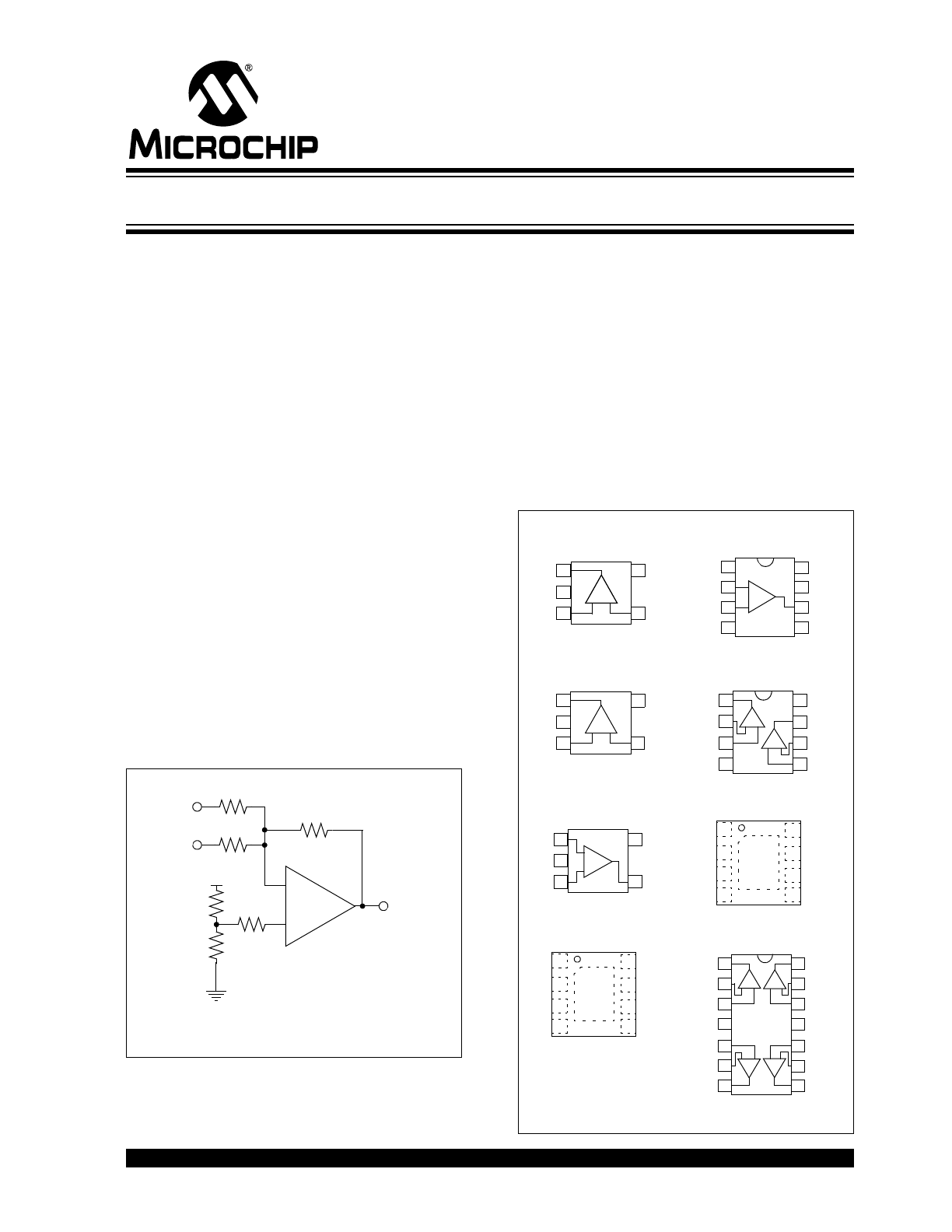
Typical Application
Description
The Microchip Technology Inc. MCP6231/1R/1U/2/4
operational amplifiers (op amps) provide wide
bandwidth for the quiescent current. The MCP6231/1R/
1U/2/4 family has a 300 kHz gain bandwidth product
and 65°C (typical) phase margin. This family operates
from a single supply voltage as low as 1.8V, while
drawing 20 µA (typical) quiescent current. In addition,
the MCP6231/1R/1U/2/4 family supports rail-to-rail
input and output swing, with a common mode input
voltage range of V
DD
+ 300 mV to V
SS
– 300 mV.
These op amps are designed in one of Microchip’s
advanced CMOS processes.
Package Types
MCP6231
V
OUT
V
IN2
–
+
V
IN1
R
G2
R
G1
R
F
R
Z
V
DD
R
X
R
Y
Summing Amplifier Circuit
4
MCP6231
1
2
3
–
+
5 V
DD
V
IN
–
V
OUT
V
SS
V
IN
+
SOT-23-5
4
1
2
3
+
5 V
DD
V
OUT
V
SS
MCP6231R
SOT-23-5
4
1
2
3
–
+
5 V
SS
V
IN
–
V
OUT
V
DD
V
IN
+
MCP6231U
SC70-5, SOT-23-5
4
1
2
3
–
+
5 V
DD
V
OUT
V
IN
+
V
SS
V
IN
–
V
IN
+
V
IN
–
MCP6231
V
SS
V
DD
V
OUT
1
2
3
4
8
7
6
5
–
+
NC
NC
NC
MSOP, PDIP, SOIC
MCP6232
MSOP, PDIP, SOIC
1
2
3
4
8
7
6
5
-
+ -
+
V
INA
_
V
INA
+
V
SS
V
OUTA
V
OUTB
V
DD
V
INB
_
V
INB
+
MCP6234
V
INA
+
V
INA
–
V
SS
1
2
3
4
14
13
12
11
-
V
OUTA
+ -
+
V
DD
V
OUTD
V
IND
–
V
IND
+
10
9
8
5
6
7
V
OUTB
V
INB
–
V
INB
+
V
INC
+
V
INC
–
V
OUTC
+
-
-
+
PDIP, SOIC, TSSOP
MCP6231
DFN *
MCP6232
V
INA
+
V
INA
_
V
SS
V
OUTB
V
INB
_
1
2
3
4
8
7
6
5 V
INB
+
V
OUTA
EP
9
V
DD
V
IN
+
V
IN
–
V
SS
V
DD
V
OUT
1
2
3
4
8
7
6
5
NC
NC
EP
9
NC
* Includes Exposed Thermal Pad (EP); see
Table 3-1
.
2x3 TDFN *
20 µA, 300 kHz Rail-to-Rail Op Amp

MCP6231/1R/1U/2/4
DS21881E-page 2
© 2009 Microchip Technology Inc.
NOTES:
© 2009 Microchip Technology Inc.
DS21881E-page 3
MCP6231/1R/1U/2/4
1.0
ELECTRICAL
CHARACTERISTICS
Absolute Maximum Ratings †
V
DD
– V
SS
........................................................................7.0V
Current at Analog Input Pins (V
IN
+, V
IN
–) .....................±2 mA
Analog Inputs (V
IN
+, V
IN
–) †† ........ V
SS
– 1.0V to V
DD
+ 1.0V
All Other Inputs and Outputs ......... V
SS
– 0.3V to V
DD
+ 0.3V
Difference Input Voltage ...................................... |V
DD
– V
SS
|
Output Short Circuit Current ................................ Continuous
Current at Output and Supply Pins ............................±30 mA
Storage Temperature ................................... –65°C to +150°C
Maximum Junction Temperature (T
J
) ......................... .+150°C
ESD Protection On All Pins (HBM; MM)
.............. ≥ 4 kV; 300V
† Notice: Stresses above those listed under “Absolute
Maximum Ratings” may cause permanent damage to the
device. This is a stress rating only and functional operation of
the device at those or any other conditions above those
indicated in the operational listings of this specification is not
implied. Exposure to maximum rating conditions for extended
periods may affect device reliability.
†† See Section 4.1.2 “Input Voltage and Current Limits”.
DC ELECTRICAL CHARACTERISTICS
Electrical Characteristics: Unless otherwise indicated, T
A
= +25°C, V
DD
= +1.8V to +5.5V, V
SS
= GND, V
CM
= V
DD
/2,
R
L
= 100 k
Ω to V
DD
/2 and V
OUT
≈ V
DD
/2.
Parameters
Sym
Min
Typ
Max
Units
Conditions
Input Offset
Input Offset Voltage
V
OS
-5.0
—
+5.0
mV
V
CM
= V
SS
Extended Temperature
V
OS
-7.0
—
+7.0
mV
T
A
= -40°C to +125°C,
V
CM
= V
SS
(Note 1)
Input Offset Drift with Temperature
ΔV
OS
/
ΔT
A
—
±3.0
—
µV/°C
T
A
= -40°C to +125°C,
V
CM
= V
SS
Power Supply Rejection Ratio
PSRR
—
83
—
dB
V
CM
= V
SS
Input Bias Current and Impedance
Input Bias Current:
I
B
—
±1.0
—
pA
At Temperature
I
B
—
20
—
pA
T
A
= +85°C
At Temperature
I
B
—
1100
—
pA
T
A
= +125°C
Input Offset Current
I
OS
—
±1.0
—
pA
Common Mode Input Impedance
Z
CM
—
10
13
||6
—
Ω||pF
Differential Input Impedance
Z
DIFF
—
10
13
||3
—
Ω||pF
Common Mode
Common Mode Input Range
V
CMR
V
SS
–
0.3
—
V
DD
+ 0.3
V
Common Mode Rejection Ratio
CMRR
61
75
—
dB
V
CM
= -0.3V to 5.3V,
V
DD
= 5V
Open-Loop Gain
DC Open-Loop Gain (large signal)
A
OL
90
110
—
dB
V
OUT
= 0.3V to V
DD
– 0.3V,
V
CM
= V
SS
Output
Maximum Output Voltage Swing
V
OL
, V
OH
V
SS
+
35
—
V
DD
– 35
mV
R
L
=10 k
Ω, 0.5V Input
Overdrive
Output Short-Circuit Current
I
SC
—
±6
—
mA
V
DD
= 1.8V
I
SC
—
±23
—
mA
V
DD
= 5.5V
Power Supply
Supply Voltage
V
DD
1.8
—
6.0
V
Quiescent Current per Amplifier
I
Q
10
20
30
µA
I
O
= 0, V
CM
= V
DD
– 0.5V
Note 1:
The SC70 package is only tested at +25°C.
2:
All parts with date codes February 2007 and later have been screened to ensure operation at V
DD
= 6.0V. However, the
other minimum and maximum specifications are measured at 1.8V and 5.5V
MCP6231/1R/1U/2/4
DS21881E-page 4
© 2009 Microchip Technology Inc.
AC ELECTRICAL CHARACTERISTICS
TEMPERATURE CHARACTERISTICS
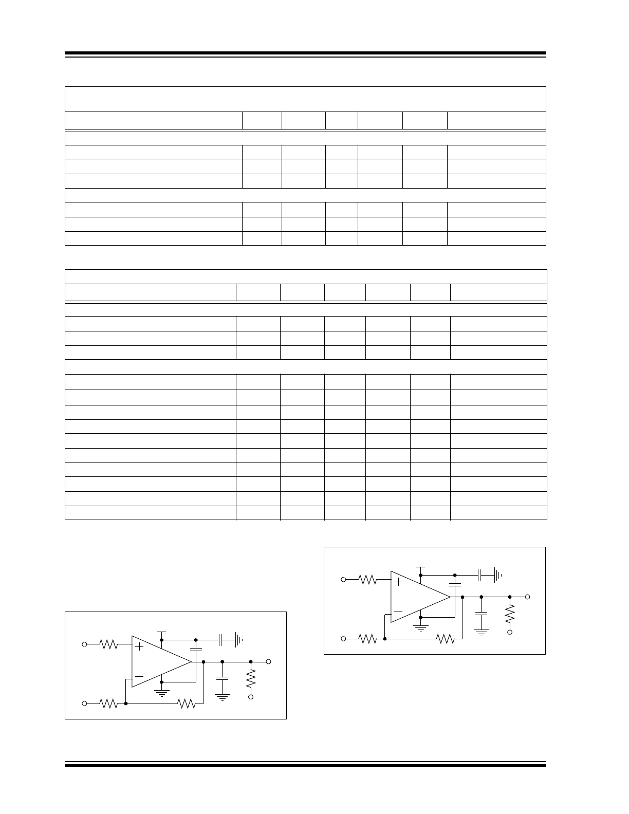
1.1
Test Circuits
The test circuits used for the DC and AC tests are
shown in
Figure 1-1
and
Figure 1-1
. The bypass
capacitors are laid out according to the rules discussed
in
Section 4.6 “PCB Surface Leakage”.
FIGURE 1-1:
AC and DC Test Circuit for
Most Non-Inverting Gain Conditions.
FIGURE 1-2:
AC and DC Test Circuit for
Most Inverting Gain Conditions.
Electrical Characteristics: Unless otherwise indicated, T
A
= +25°C, V
DD
= +1.8 to 5.5V, V
SS
= GND, V
CM
= V
DD
/2,
V
OUT
≈ V
DD
/2, R
L
= 100 k
Ω to V
DD
/2 and C
L
= 60 pF.
Parameters
Sym
Min
Typ
Max
Units
Conditions
AC Response
Gain Bandwidth Product
GBWP
—
300
—
kHz
Phase Margin
PM
—
65
—
°
G = +1 V/V
Slew Rate
SR
—
0.15
—
V/µs
Noise
Input Noise Voltage
E
ni
—
6.0
—
µV
P-P
f = 0.1 Hz to 10 Hz
Input Noise Voltage Density
e
ni
—
52
—
nV/
√Hz f = 1 kHz
Input Noise Current Density
i
ni
—
0.6
—
fA/
√Hz f = 1 kHz
Electrical Characteristics: Unless otherwise indicated, V
DD
= +1.8V to +5.5V and V
SS
= GND.
Parameters
Sym
Min
Typ
Max
Units
Conditions
Temperature Ranges
Extended Temperature Range
T
A
-40
—
+125
°C
Operating Temperature Range
T
A
-40
—
+125
°C
Note
Storage Temperature Range
T
A
-65
—
+150
°C
Thermal Package Resistances
Thermal Resistance, 5L-SC70
θ
JA
—
331
—
°C/W
Thermal Resistance, 5L-SOT-23
θ
JA
—
256
—
°C/W
Thermal Resistance, 8L-DFN
θ
JA
—
84.5
—
°C/W
Thermal Resistance, 8L-MSOP
θ
JA
—
206
—
°C/W
Thermal Resistance, 8L-TDFN
θ
JA
—
41
—
°C/W
Thermal Resistance, 8L-PDIP
θ
JA
—
85
—
°C/W
Thermal Resistance, 8L-SOIC
θ
JA
—
163
—
°C/W
Thermal Resistance, 14L-PDIP
θ
JA
—
70
—
°C/W
Thermal Resistance, 14L-SOIC
θ
JA
—
120
—
°C/W
Thermal Resistance, 14L-TSSOP
θ
JA
—
100
—
°C/W
Note:
The internal Junction Temperature (T
J
) must not exceed the Absolute Maximum specification of +150°C.
V
DD
MCP623X
R
G
R
F
R
N
V
OUT
V
IN
V
DD
/2
1 µF
C
L
R
L
V
L
0.1 µF
V
DD
MCP623X
R
G
R
F
R
N
V
OUT
V
DD
/2
V
IN
1 µF
C
L
R
L
V
L
0.1 µF
© 2009 Microchip Technology Inc.
DS21881E-page 5
MCP6231/1R/1U/2/4
2.0
TYPICAL PERFORMANCE CURVES
Note: Unless otherwise indicated, T
A
= +25°C, V
DD
= +1.8V to +5.5V, V
SS
= GND, V
CM
= V
DD
/2, V
OUT
≈ V
DD
/2,
R
L
= 100 k
Ω to V
DD
/2 and C
L
= 60 pF.
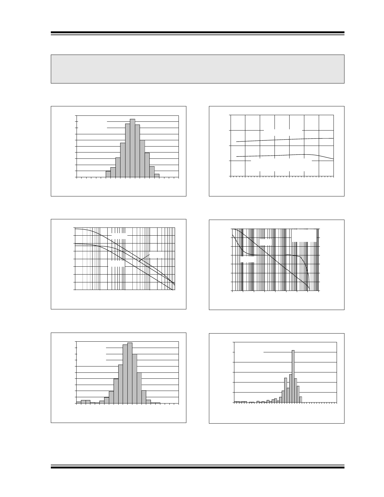
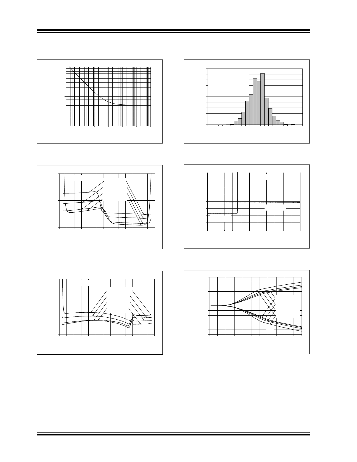
FIGURE 2-1:
Input Offset Voltage.
FIGURE 2-2:
PSRR, CMRR vs.
Frequency.
FIGURE 2-3:
Input Bias Current at +85°C.
FIGURE 2-4:
CMRR, PSRR vs. Ambient
Temperature.
FIGURE 2-5:
Open-Loop Gain, Phase vs.
Frequency.
FIGURE 2-6:
Input Bias Current at
+125°C.
Note:
The graphs and tables provided following this note are a statistical summary based on a limited number of
samples and are provided for informational purposes only. The performance characteristics listed herein
are not tested or guaranteed. In some graphs or tables, the data presented may be outside the specified
operating range (e.g., outside specified power supply range) and therefore outside the warranted range.
0%
2%
4%
6%
8%
10%
12%
14%
16%
18%
20%
-5
-4
-3
-2
-1
0
1
2
3
4
5
Input Offset Voltage (mV)
P
e
rcent
age of Occurrences
630 Samples
V
CM
= V
SS
20
30
40
50
60
70
80
90
100
1.E+01
1.E+02
1.E+03
1.E+04
1.E+05
Frequency (Hz)
PSRR, CMRR (
d
B)
10
1k
10k
100k
100
PSRR+
PSRR-
CMRR
0%
2%
4%
6%
8%
10%
12%
14%
16%
18%
20%
0
6
12
18
24
30
36
42
Input Bias Current (pA)
P
e
rcentage of
Occurrences
630 Samples
V
CM
= V
DD
/2
T
A
= +85°C
70
75
80
85
90
-50
-25
0
25
50
75
100
125
Ambient Temperature (°C)
CM
RR, PSRR
(
d
B)
PSRR (V
CM
= V
SS
)
CMRR (V
CM
= -0.3V to +5.3V,
V
DD
= 5.0V)
-20
0
20
40
60
80
100
120
1.E-
01
1.E+
00
1.E+
01
1.E+
02
1.E+
03
1.E+
04
1.E+
05
1.E+
06
1.E+
07
Frequency (Hz)
Open-
L
oop Gain (dB)
-210
-180
-150
-120
-90
-60
-30
0
Open
-Loop P
h
ase (°)
R
L
= 10 kΩ
V
CM
= V
DD
/2
0.1
1
10 100 1k 10k 100k 1M 10M
Gain
Phase
0%
5%
10%
15%
20%
25%
30%
0.
0
0.
2
0.
4
0.
6
0.
8
1.
0
1.
2
1.
4
1.
6
1.
8
2.
0
Input Bias Current (nA)
Percent
age of Occurrences
632 Samples
V
CM
= V
DD
/2
T
A
= +125°C
MCP6231/1R/1U/2/4
DS21881E-page 6
© 2009 Microchip Technology Inc.
Note: Unless otherwise indicated, T
A
= +25°C, V
DD
= +1.8V to +5.5V, V
SS
= GND, V
CM
= V
DD
/2, V
OUT
≈ V
DD
/2,
R
L
= 100 k
Ω to V
DD
/2 and C
L
= 60 pF.
FIGURE 2-7:
Input Noise Voltage Density
vs. Frequency.
FIGURE 2-8:
Input Offset Voltage vs.
Common Mode Input Voltage at V
DD
= 1.8V.
FIGURE 2-9:
Input Offset Voltage vs.
Common Mode Input Voltage at V
DD
= 5.5V.
FIGURE 2-10:
Input Offset Voltage Drift.
FIGURE 2-11:
Input Offset Voltage vs.
Output Voltage.
FIGURE 2-12:
Output Short-Circuit Current
vs. Ambient Temperature.
10
100
1,000
1.E-01 1.E+0
0
1.E+0
1
1.E+0
2
1.E+0
3
1.E+0
4
1.E+0
5
Frequency (Hz)
Input
Noise V
o
lt
age Density
(n
V
/√
Hz)
0.1
100
1k
10k
100k
10
1
150
250
350
450
550
-0
.4
-0
.2
0.
0
0.
2
0.
4
0.
6
0.
8
1.
0
1.
2
1.
4
1.
6
1.
8
2.
0
2.
2
Common Mode Input Voltage (V)
In
p
u
t Of
fs
et
Vo
lt
ag
e (µ
V
)
V
DD
= 1.8V
T
A
= -40°C
T
A
= +25°C
T
A
= +85°C
T
A
= +125°C
-200
-150
-100
-50
0
50
100
150
200
-0.5
0.0
0.5
1.0
1.5
2.0
2.5
3.0
3.5
4.0
4.5
5.0
5.5
6.0
Common Mode Input Voltage (V)
Input Offset V
o
ltage (µV
)
V
DD
= 5.5 V
T
A
= +125°C
T
A
= +85°C
T
A
= +25°C
T
A
= -40°C
0%
2%
4%
6%
8%
10%
12%
14%
16%
18%
20%
-1
2
-1
0
-8
-6
-4
-2
0
2
4
6
8
10
12
Input Offset Voltage Drift (µV/°C)
P
e
rcentage of
Occurrences
628 Samples
V
CM
= V
SS
T
A
= -40°C to +125°C
-300
-250
-200
-150
-100
-50
0
50
100
0.0 0.5 1.0 1.5 2.0 2.5 3.0 3.5 4.0 4.5 5.0 5.5
Output Voltage (V)
Input
Offset Volt
ag
e (
µ
V)
V
DD
= 1.8V
V
CM
= V
SS
V
DD
= 5.5V
-30
-25
-20
-15
-10
-5
0
5
10
15
20
25
30
0.0 0.5 1.0 1.5 2.0 2.5 3.0 3.5 4.0 4.5 5.0 5.5
Power Supply Voltage (V)
Output
S
hort-
Circuit
Current
(m
A
)
T
A
= +125°C
T
A
= +85°C
T
A
= +25°C
T
A
= -40°C
+I
SC
-I
SC
© 2009 Microchip Technology Inc.
DS21881E-page 7
MCP6231/1R/1U/2/4
Note: Unless otherwise indicated, T
A
= +25°C, V
DD
= +1.8V to +5.5V, V
SS
= GND, V
CM
= V
DD
/2, V
OUT
≈ V
DD
/2,
R
L
= 100 k
Ω to V
DD
/2 and C
L
= 60 pF.
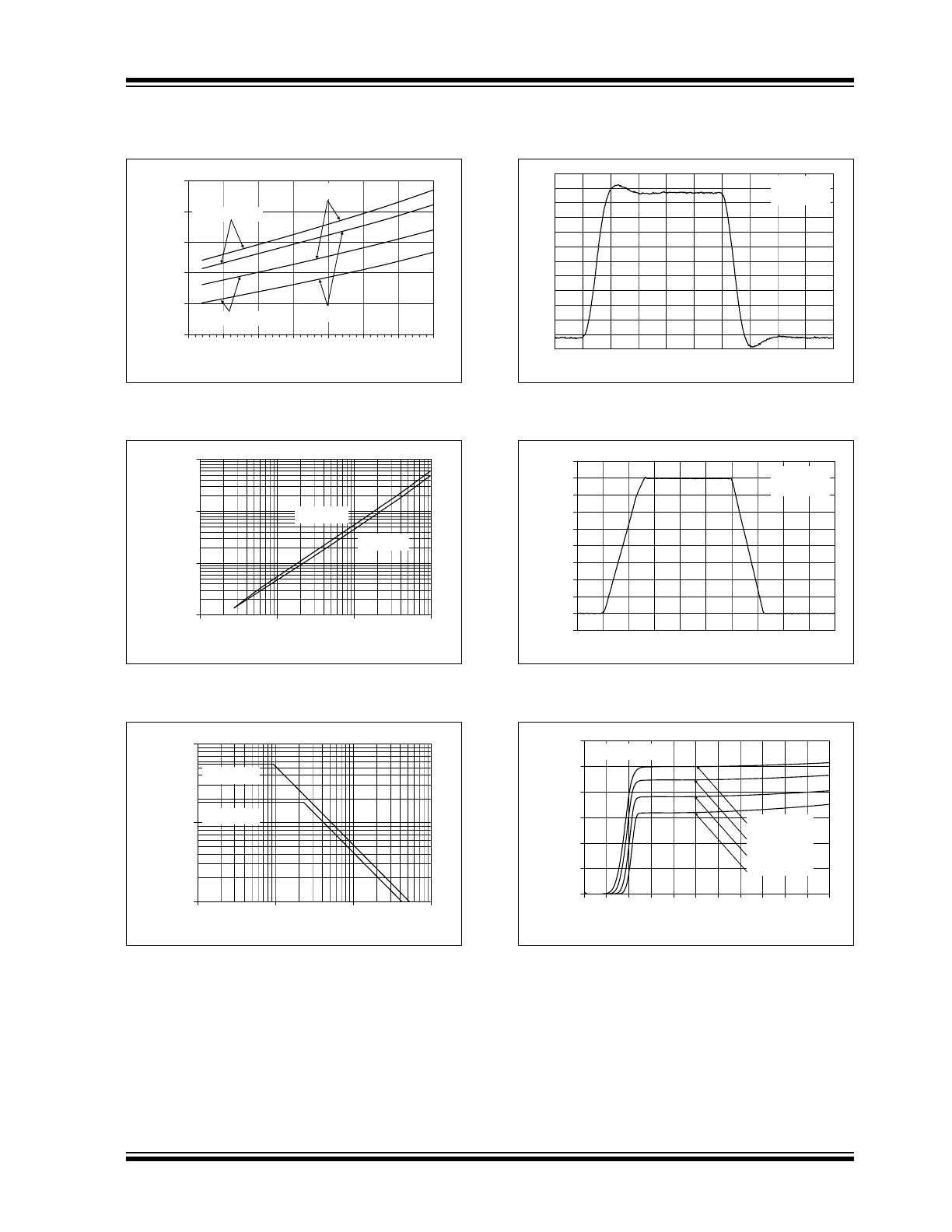
FIGURE 2-13:
Slew Rate vs. Ambient
Temperature.
FIGURE 2-14:
Output Voltage Headroom
vs. Output Current Magnitude.
FIGURE 2-15:
Maximum Output Voltage
Swing vs. Frequency.
FIGURE 2-16:
Small-Signal, Non-Inverting
Pulse Response.
FIGURE 2-17:
Large-Signal, Non-Inverting
Pulse Response.
FIGURE 2-18:
Quiescent Current vs.
Power Supply Voltage.
0.05
0.10
0.15
0.20
0.25
0.30
-50
-25
0
25
50
75
100
125
Ambient Temperature (°C)
Sle
w
Ra
te
(V/µ
s
)
Falling Edge
Rising Edge
V
DD
= 1.8V
V
DD
= 5.5V
1
10
100
1,000
1.E-02
1.E-01
1.E+00
1.E+01
Output Current Magnitude (A)
Output
Volt
ag
e He
adroom
(m
V
)
V
DD
– V
OH
10m
1m
V
OL
– V
SS
100µ
10µ
0.1
1
10
1.E+03
1.E+04
1.E+05
1.E+06
Frequency (Hz)
Max
. Output Voltage
Swing
(V
P-P
)
V
DD
= 5.5V
V
DD
= 1.8V
1k
10k
100k
1M
Time (2 µs/div)
Output
V
o
lta
g
e (10
mV/div
)
G = +1 V/V
R
L
= 10 kΩ
0.0
0.5
1.0
1.5
2.0
2.5
3.0
3.5
4.0
4.5
5.0
Time (20 µs/div)
Output
Volt
ag
e (
V
)
V
DD
= 5.0V
G = +1 V/V
0
5
10
15
20
25
30
0.0 0.5 1.0 1.5 2.0 2.5 3.0 3.5 4.0 4.5 5.0 5.5
Power Supply Voltage (V)
Q
u
ie
sc
ent
Cur
re
nt
per Amplifier (µA)
V
CM
= 0.9V
DD
T
A
= +125°C
T
A
= +85°C
T
A
= +25°C
T
A
= -40°C
MCP6231/1R/1U/2/4
DS21881E-page 8
© 2009 Microchip Technology Inc.
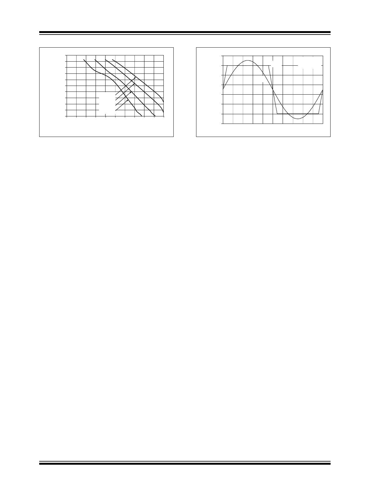
FIGURE 2-19:
Measured Input Current vs.
Input Voltage (below V
SS
).
FIGURE 2-20:
The MCP6231/1R/1U/2/4
Show No Phase Reversal.
1.E-12
1.E-11
1.E-10
1.E-09
1.E-08
1.E-07
1.E-06
1.E-05
1.E-04
1.E-03
1.E-02
-1.0 -0.9 -0.8 -0.7 -0.6 -0.5 -0.4 -0.3 -0.2 -0.1 0.0
Input Voltage (V)
In
p
u
t Curre
nt Mag
n
it
ude
(
A
)
+125°C
+85°C
+25°C
-40°C
10m
1m
100µ
10µ
1µ
100n
10n
1n
100p
10p
1p
-1.0
0.0
1.0
2.0
3.0
4.0
5.0
6.0
Time (1 ms/div)
In
pu
t,
O
u
tp
u
t V
o
lt
ages
(
V
)
V
OUT
V
IN
V
DD
= 5.0V
G = +2 V/V
© 2009 Microchip Technology Inc.
DS21881E-page 9
MCP6231/1R/1U/2/4
3.0
PIN DESCRIPTIONS
Descriptions of the pins are listed in
Table 3-1
(single op amps) and
Table 3-2
(dual and quad op amps).
TABLE 3-1:
PIN FUNCTION TABLE FOR SINGLE OP AMPS
TABLE 3-2:
PIN FUNCTION TABLE FOR DUAL AND QUAD OP AMPS
3.1
Analog Outputs
The output pins are low-impedance voltage sources.
3.2
Analog Inputs
The non-inverting and inverting inputs are
high-impedance CMOS inputs with low bias currents.
3.3
Power Supply (V
SS
and V
DD
)
The positive power supply (V
DD
) is 1.8V to 6.0V higher
than the negative power supply (V
SS
). For normal
operation, the other pins are between V
SS
and V
DD
.
Typically, these parts are used in a single (positive)
supply configuration. In this case, V
SS
is connected to
ground and V
DD
is connected to the supply. V
DD
will
need bypass capacitors.
3.4
Exposed Thermal Pad (EP)
There is an internal electrical connection between the
Exposed Thermal Pad (EP) and the V
SS
pin; they must
be connected to the same potential on the Printed
Circuit Board (PCB).
MCP6231
MCP6231R
MCP6231U
Symbol
Description
DFN, MSOP,
PDIP, SOIC
SOT-23-5
SOT-23-5
SOT-23-5
SC70
6
1
1
4
V
OUT
Analog Output
2
4
4
3
V
IN
–
Inverting Input
3
3
3
1
V
IN
+
Non-inverting Input
7
5
2
5
V
DD
Positive Power Supply
4
2
5
2
V
SS
Negative Power Supply
1, 5, 8
—
—
—
NC
No Internal Connection
9
—
—
—
EP
Exposed Thermal Pad (EP); must be
connected to V
SS
.
MCP6232
MCP6234
Symbol
Description
MSOP, PDIP,
SOIC, TDFN
PDIP, SOIC, TSSOP
1
1
V
OUTA
Analog Output (op amp A)
2
2
V
INA
–
Inverting Input (op amp A)
3
3
V
INA
+
Non-inverting Input (op amp A)
8
4
V
DD
Positive Power Supply
5
5
V
INB
+
Non-inverting Input (op amp B)
6
6
V
INB
–
Inverting Input (op amp B)
7
7
V
OUTB
Analog Output (op amp B)
—
8
V
OUTC
Analog Output (op amp C)
—
9
V
INC
–
Inverting Input (op amp C)
—
10
V
INC
+
Non-inverting Input (op amp C)
4
11
V
SS
Negative Power Supply
—
12
V
IND
+
Non-inverting Input (op amp D)
—
13
V
IND
–
Inverting Input (op amp D)
—
14
V
OUTD
Analog Output (op amp D)
9
—
—
Exposed Thermal Pad (EP); must be connected to V
SS
.

MCP6231/1R/1U/2/4
DS21881E-page 10
© 2009 Microchip Technology Inc.
NOTES: