
2002-2012 Microchip Technology Inc.
DS20092B-page 1
TC77
Features
• Digital Temperature Sensing in 5-Pin SOT-23A
and 8-Pin SOIC Packages
• Outputs Temperature as a 13-Bit Digital Word
• SPI and MICROWIRE™ Compatible Interface
• Solid State Temperature Sensing
• ±1°C (max.) accuracy from +25°C to +65°C
• ±2°C (max.) accuracy from -40°C to +85°C
• ±3°C (max.) accuracy from -55°C to +125°C
• 2.7V to 5.5V Operating Range
• Low Power
- 250 µA (typ.) Continuous Conversion Mode
- 0.1 µA (typ.) Shutdown Mode
Typical Applications
• Thermal Protection for Hard Disk Drives and
Other PC Peripherals
• PC Card Devices for Notebook Computers
• Low Cost Thermostat Controls
• Industrial Control
• Office Equipment
• Cellular Phones
• Thermistor Replacement
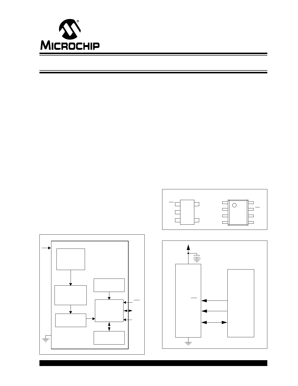
Block Diagram
Description
The TC77 is a serially accessible digital temperature
sensor particularly suited for low cost and small form-
factor applications. Temperature data is converted from
the internal thermal sensing element and made avail-
able at anytime as a 13-bit two’s compliment digital
word. Communication with the TC77 is accomplished
via a SPI and MICROWIRE compatible interface. It has
a 12-bit plus sign temperature resolution of 0.0625°C
per Least Significant Bit (LSb). The TC77 offers a tem-
perature accuracy of ±1.0°C (max.) over the tempera-
ture range of +25°C to +65°C. When operating, the
TC77 consumes only 250 µA (typ.). The TC77’s Con-
figuration register can be used to activate the low
power Shutdown mode, which has a current consump-
tion of only 0.1 µA (typ.). Small size, low cost and ease
of use make the TC77 an ideal choice for implementing
thermal management in a variety of systems.
Package Types
Typical Application
TC77
Diode
Temperature
Sensor
V
DD
SCK
CS
Serial
Port
Interface
SI/O
13-Bit
Sigma Delta
A/D Converter
Register
Temperature
Register
Internal
Configuration
Manufacturer
ID Register
V
SS
SOT-23-5
1
SOIC
1
V
DD
V
SS
SCK
SI/O
CS
TC77
TC77
SCK
SI/O
V
SS
NC
CS
V
DD
NC
NC
AN0
SCK
SDI
CS
SCK
SI/O
TC77
0.1µF
V
DD
V
SS
V
DD
PIC
®
MCU
Thermal Sensor with SPI Interfa
ce
TC77
DS20092B-page 2
2002-2012 Microchip Technology Inc.
1.0
ELECTRICAL
CHARACTERISTICS
1.1
Absolute Maximum Ratings †
V
DD
........................................................................6.0V
All inputs and outputs w.r.t. V
SS
..... -0.3V to V
DD
+0.3V
Storage temperature ..........................-65°C to +150°C
Ambient temp. with power applied .....-55°C to +125°C
Junction Temperature......................................... 150°C
ESD protection on all pins:
Human Body Model (HBM).............................. >4 kV
Machine Model (MM) ......................................>200V
† Notice: Stresses above those listed under "Maximum
Ratings" may cause permanent damage to the device. This is
a stress rating only and functional operation of the device at
those or any other conditions above those indicated in the
operation listings of this specification is not implied. Exposure
to maximum rating conditions for extended periods may affect
device reliability.
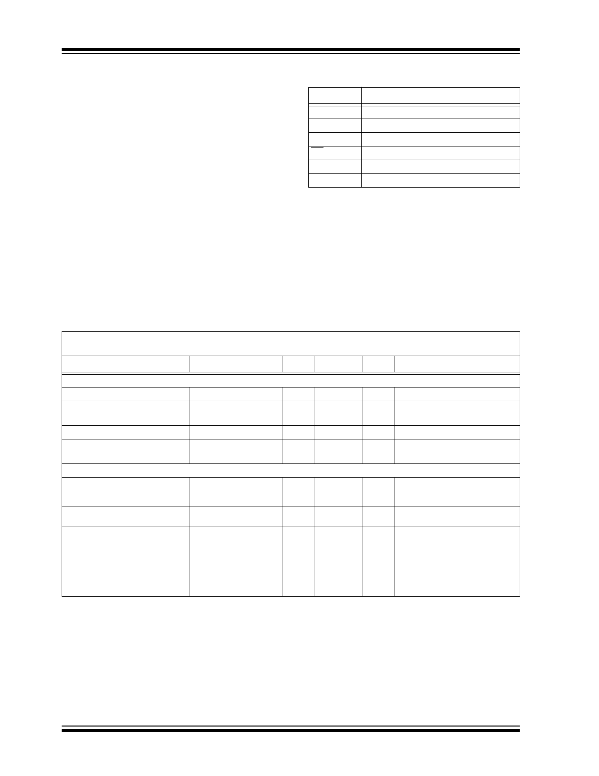
PIN FUNCTION TABLE
Name
Function
SI/O
Serial Data Pin
SCK
Serial Clock
V
SS
Ground
CS
Chip Select (Active-Low)
NC
No Connection
V
DD
Power Supply
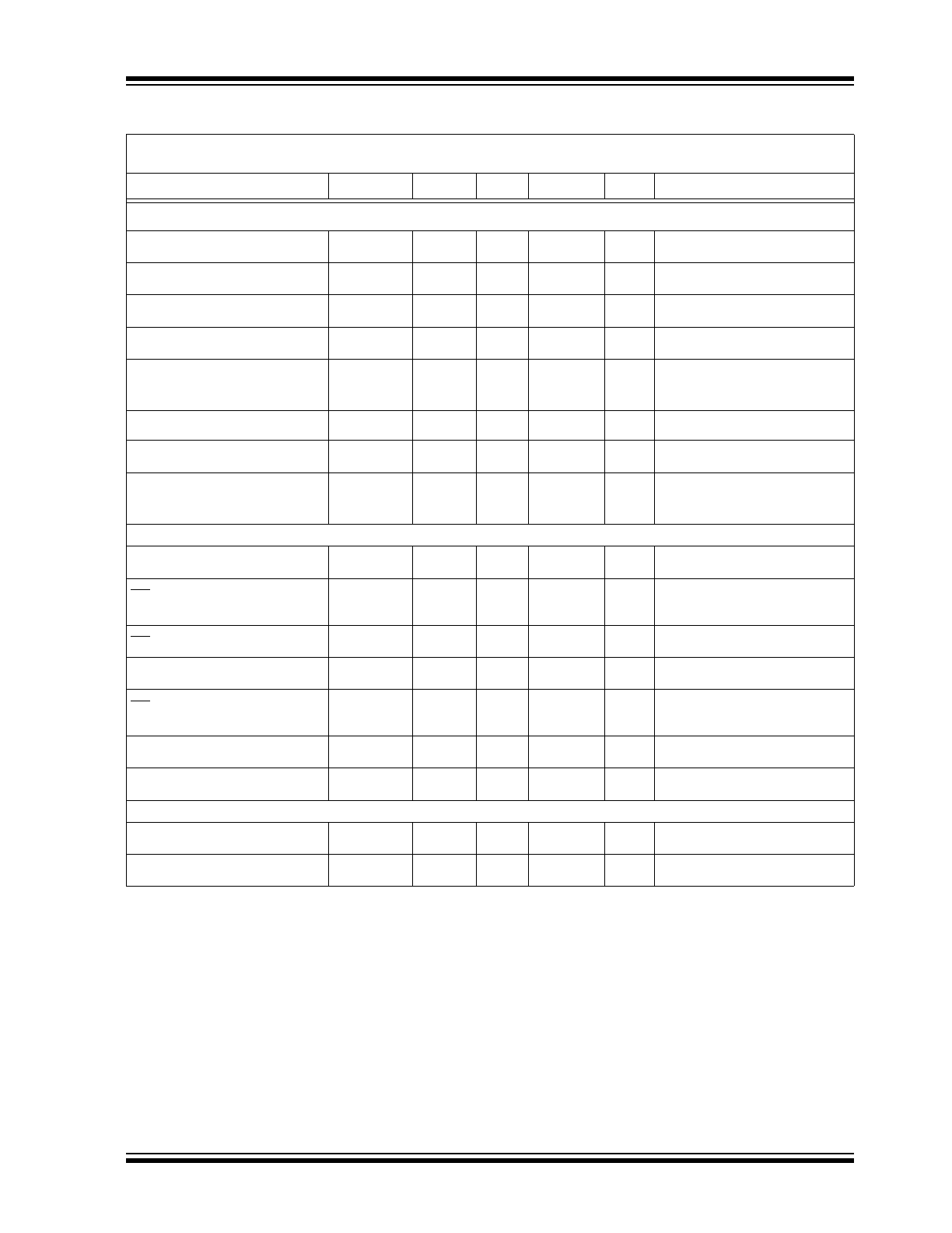
DC CHARACTERISTICS
Electrical Specifications: Unless otherwise noted, all parameters apply at V
DD
= 2.7V to 5.5V and
T
A
= -55°C to +125°C.
Parameters
Sym
Min
Typ
Max
Units
Conditions
Power Supply
Operating Voltage Range
V
DD
2.7
—
5.5
V
Note 1
Operating Current
I
DD
—
250
400
µA
Continuous Temperature
Conversion Mode
Power-On Reset Threshold
V
POR
1.2
1.6
2.2
V
V
DD
falling or rising edge
Standby Supply Current
I
DD-
STANDBY
—
0.1
1.0
µA
Shutdown Mode
Temperature to Bits Converter
Resolution
—
13
—
Bits
ADC LSb = 0.0625°C/bit
(Note 4)
Temperature Conversion Time
t
CT
—
300
400
ms
Temperature Accuracy
(Note 1)
T
ERR
-1.0
-2.0
-3.0
—
—
—
+1.0
+2.0
+3.0
°C
+25°C < T
A
< +65°C
-40°C < T
A
< +85°C
-55°C < T
A
< +125°C
TC77-3.3MXX: V
DD
= 3.3V
TC77-5.0MXX: V
DD
= 5.0V
Note 1: The TC77-3.3MXX and TC77-5.0MXX will operate from a supply voltage of 2.7V to 5.5V. However, the tem-
perature accuracy of the TC77-3.3MXX and TC77-5.0MXX is specified at the nominal operating voltages of
3.3V and 5.0V, respectively. As V
DD
varies from the nominal operating value, the accuracy may be
degraded (Refer to Figures 2-6 and 2-7).
2: All time measurements are measured with respect to the 50% point of the signal.
3: Load Capacitance, C
L
= 80 pF, is used for AC timing measurements of output signals.
4: Resolution = Temperature Range/No. of Bits = (+255°C – -256°C) / (2
13
)
Resolution = 512/8192 = 0.0625°C/Bit
2002-2012 Microchip Technology Inc.
DS20092B-page 3
TC77
Digital Input/Output
High Level Input Voltage
V
IH
0.7 V
DD
—
V
DD
+ 0.3
V
Low Level Input Voltage
V
IL
-0.3
—
0.3 V
DD
V
High Level Output Voltage
V
OH
2.4
—
—
V
I
OH
= -400 µA
Low Level Output Voltage
V
OL
—
—
0.4
V
I
OL
= +2 mA
Input Current
I
IN(0),
I
IN(1)
-1.0
-1.0
—
—
+1.0
+1.0
µA
V
IN
= GND
V
IN
= V
DD
Input Hysteresis
0.35
0.8
—
V
SI/O, SCK
Pin Capacitance
C
IN
, C
OUT
—
20
—
pF
Tri-state Output Leakage
Current
I
O_LEAK
-1.0
—
—
—
—
+1.0
µA
V
O
= GND
V
O
= V
DD
Serial Port AC Timing (Notes 2, 3)
Clock Frequency
f
CLK
DC
—
7.0
MHz
CS Fall to First Rising SCK
Edge
t
CS-SCK
100
—
—
ns
CS Low to Data Out Delay
t
CS-SI/O
—
—
70
ns
SCK Fall to Data Out Delay
t
DO
—
—
100
ns
CS High to Data Out
Tri-state
t
DIS
—
—
200
ns
SCK High to Data In Hold Time
t
HD
50
—
—
ns
Data In Set-up Time
t
SU
30
—
—
ns
Thermal Package Resistance
Thermal Resistance, SOT23-5
JA
—
230
—
°C/W
Thermal Resistance, 8L-SOIC
JA
—
163
—
°C/W
DC CHARACTERISTICS (CONTINUED)
Electrical Specifications: Unless otherwise noted, all parameters apply at V
DD
= 2.7V to 5.5V and
T
A
= -55°C to +125°C.
Parameters
Sym
Min
Typ
Max
Units
Conditions
Note 1: The TC77-3.3MXX and TC77-5.0MXX will operate from a supply voltage of 2.7V to 5.5V. However, the tem-
perature accuracy of the TC77-3.3MXX and TC77-5.0MXX is specified at the nominal operating voltages of
3.3V and 5.0V, respectively. As V
DD
varies from the nominal operating value, the accuracy may be
degraded (Refer to Figures 2-6 and 2-7).
2: All time measurements are measured with respect to the 50% point of the signal.
3: Load Capacitance, C
L
= 80 pF, is used for AC timing measurements of output signals.
4: Resolution = Temperature Range/No. of Bits = (+255°C – -256°C) / (2
13
)
Resolution = 512/8192 = 0.0625°C/Bit
TC77
DS20092B-page 4
2002-2012 Microchip Technology Inc.
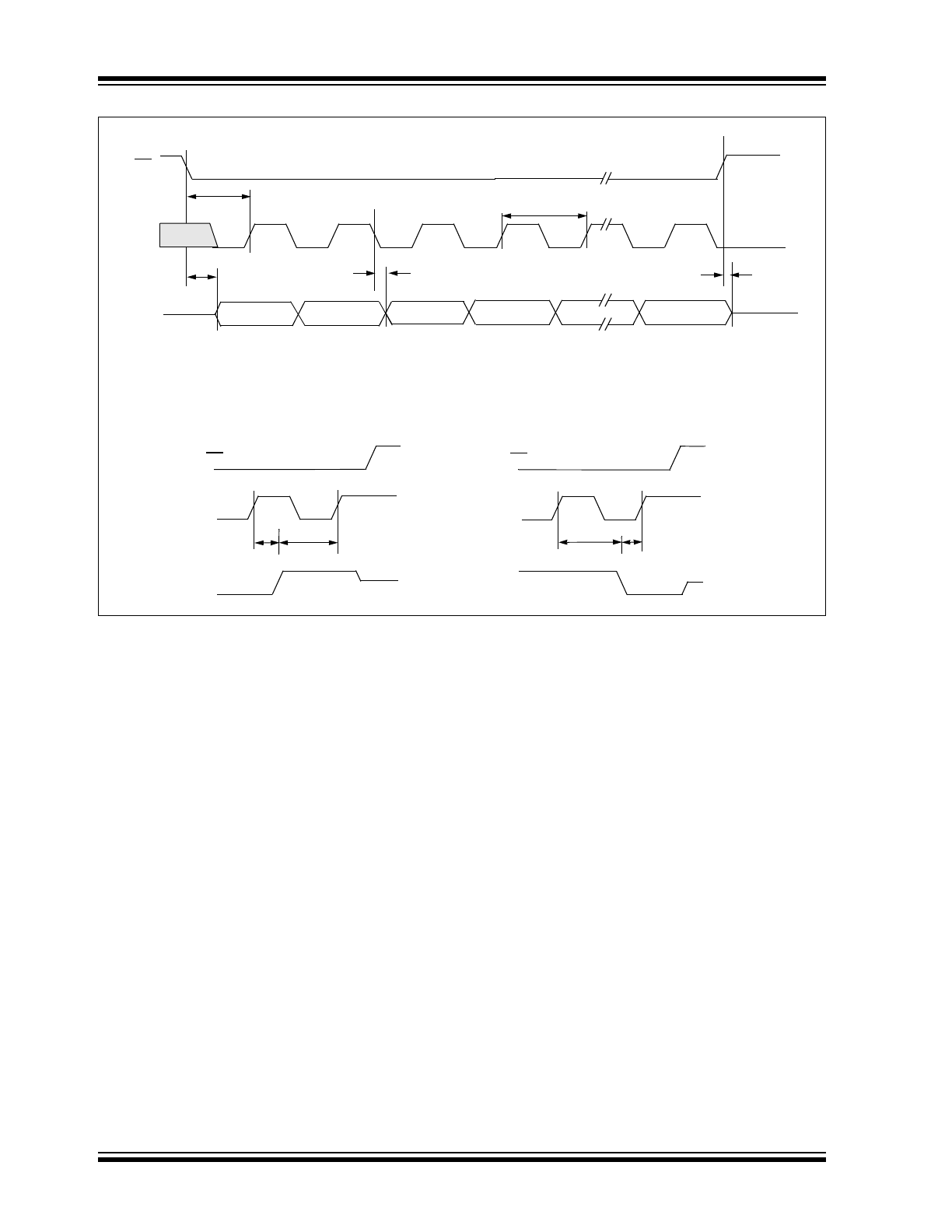
FIGURE 1-1:
Timing Diagrams.
CS
SCK
1/f
CLK
SI/O
t
DO
LSb
t
DIS
HI-Z
Data Output Timing
MSb
t
CS-SI/O
t
HD
t
SU
SI/O
SCK
CS
HI-Z
SI/O
SCK
CS
HI-Z
t
HD
t
SU
HI-Z
t
CS-SCK
SI/O Data Input Set-up and Hold Timing (Data is clocked on the rising edge of SCK)
2002-2012 Microchip Technology Inc.
DS20092B-page 5
TC77
2.0
TYPICAL PERFORMANCE CURVES
Note: Unless otherwise indicated, all parameters apply at V
DD
= 3.3V for the TC77-3.3MXX and V
DD
= 5.0V for the TC77-
5.0MXX, and T
A
= -55°C to +125°C. The TC77-3.3MXX and TC77-5.0MXX will operate from a supply voltage of 2.7V
to 5.5V. However, the temperature accuracy of the TC77-3.3MXX and TC77-5.0MXX is specified at the nominal oper-
ating voltages of 3.3V and 5.0V, respectively.
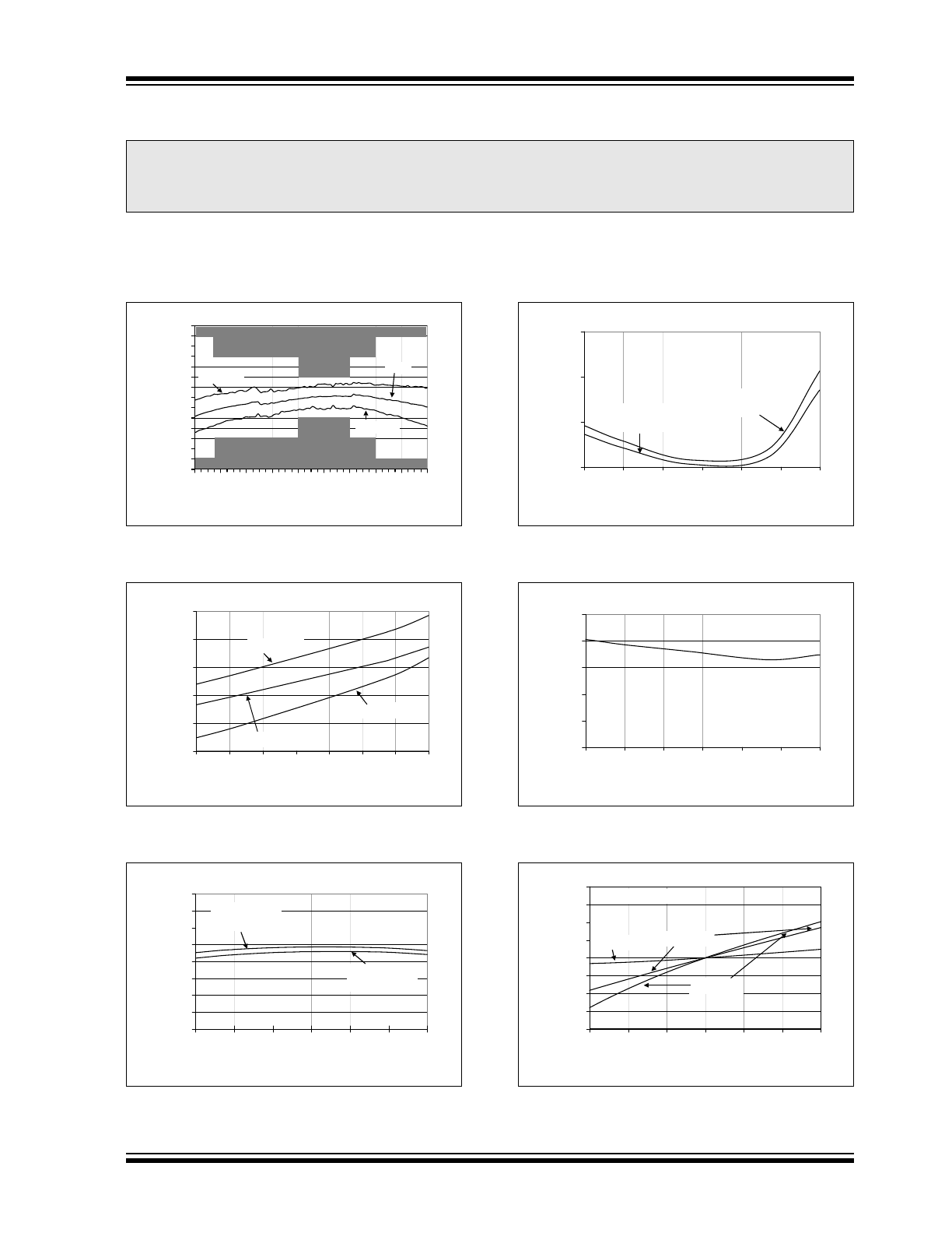
FIGURE 2-1:
Accuracy vs. Temperature
(TC77-XXMXX)
.
FIGURE 2-2:
Supply Current vs. Supply
Voltage (TC77-XXMXX).
FIGURE 2-3:
Supply Current vs.
Temperature.
FIGURE 2-4:
Shutdown Current vs.
Temperature.
FIGURE 2-5:
Power-On Reset Voltage vs.
Temperature (TC77-XXMXX).
FIGURE 2-6:
Temperature Accuracy vs.
Supply Voltage (TC77-3.3MXX).
Note:
The graphs and tables provided following this note are a statistical summary based on a limited number of
samples and are provided for informational purposes only. The performance characteristics listed herein
are not tested or guaranteed. In some graphs or tables, the data presented may be outside the specified
operating range (e.g., outside specified power supply range) and therefore outside the warranted range.
-3.5
-3
-2.5
-2
-1.5
-1
-0.5
0
0.5
1
1.5
2
2.5
3
3.5
-55 -35 -15
5
25
45
65
85 105 125
Reference Temperature (°C)
Temperature Error (°C)
Upper Specification Limit
Lower Specification Limit
Mean + 3V
Mean - 3V
Mean
200
210
220
230
240
250
2.7
3.1
3.5
3.9
4.3
4.7
5.1
5.5
Supply Voltage (V)
Suppl
y Cur
re
nt
(
µ
A)
T
A
= +25°C
T
A
= +125°C
T
A
= -55°C
0
50
100
150
200
250
300
350
400
-55
-25
5
35
65
95
125
Temperature (°C)
Suppl
y Cur
re
nt
(
µ
A)
TC77-5.0MXX
V
DD
= 5.0 V
TC77-3.3MXX
V
DD
= 3.3 V
0.0
0.1
0.2
0.3
-55
-25
5
35
65
95
125
Temperature (°C)
Shut
dow
n Cur
re
nt
(
µ
A)
TC77-5.0MXX
V
DD
= 5.0 V
TC77-3.3MXX
V
DD
= 3.3 V
0.0
0.5
1.0
1.5
2.0
2.5
-55
-25
5
35
65
95
125
Temperature (°C)
Pow
e
r-
O
n
R
eset
Vol
tage (
V
)
-0.4
-0.3
-0.2
-0.1
0
0.1
0.2
0.3
0.4
3
3.1
3.2
3.3
3.4
3.5
3.6
Supply Voltage (V)
Tem
p
er
at
ur
e C
h
ange (
°C
)
TC77-3.3MXX
T
A
= -25°C
T
A
= +25°C
T
A
= +85°C
TC77
DS20092B-page 6
2002-2012 Microchip Technology Inc.
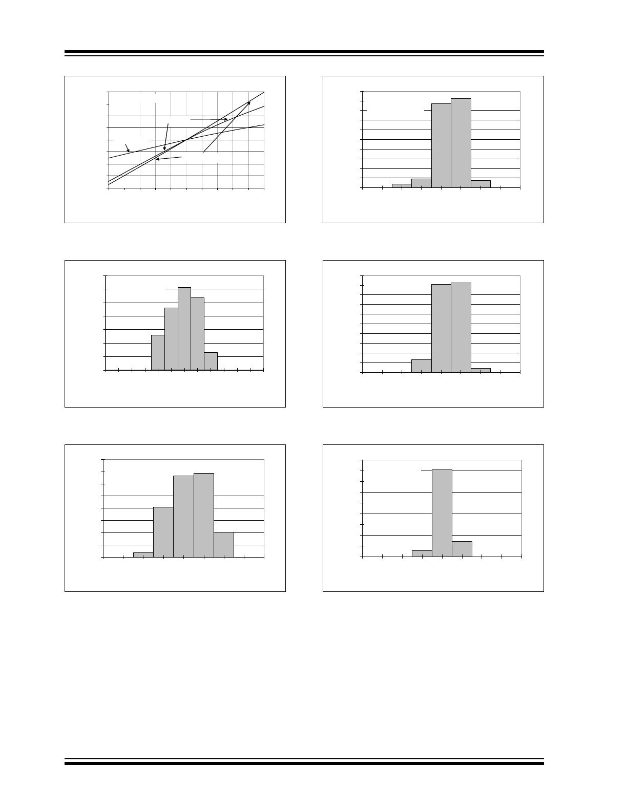
FIGURE 2-7:
Temperature Accuracy vs.
Supply Voltage (TC77-5.0MXX).
FIGURE 2-8:
Histogram of Temperature
Accuracy at -55 Degrees C (TC77-XXMXX).
FIGURE 2-9:
Histogram of Temperature
Accuracy at -40 Degrees C (TC77-XXMXX).
FIGURE 2-10:
Histogram of Temperature
Accuracy at +25 Degrees C (TC77-XXMXX).
FIGURE 2-11:
Histogram of Temperature
Accuracy at +65 Degrees C (TC77-XXMXX).
FIGURE 2-12:
Histogram of Temperature
Accuracy at +85 Degrees C (TC77-XXMXX).
-0.4
-0.3
-0.2
-0.1
0
0.1
0.2
0.3
0.4
4.5 4.6 4.7 4.8 4.9
5
5.1 5.2 5.3 5.4 5.5
Supply Voltage (V)
Tem
p
er
at
ur
e C
h
ange (
°C
)
TC77-5.0MXX
T
A
= -25°C
T
A
= +25°C
T
A
= +85°C
0
5
10
15
20
25
30
35
-3 -2.5 -2 -1.5 -1 -0.5
0
0.5
1
1.5
2
2.5
3
Temperature Error (°C)
P
e
rcen
ta
g
e
o
f O
ccu
ra
n
ces (
%
)
Sample Size = 108
T
A
= -55°C
0
5
10
15
20
25
30
35
40
-2
-1.5
-1
-0.5
0
0.5
1
1.5
2
Temperature Error (°C)
P
e
rcen
ta
g
e
o
f O
ccu
ra
n
ces (
%
)
Sample Size = 108
T
A
= -40°C
0
5
10
15
20
25
30
35
40
45
50
-1
-0.75
-0.5
-0.25
0
0.25
0.5
0.75
1
Temperature Error (°C)
P
e
rcen
ta
g
e
o
f O
ccu
ra
n
ces (
%
)
Sample Size = 108
T
A
= +25°C
0
5
10
15
20
25
30
35
40
45
50
-1
-0.75
-0.5
-0.25
0
0.25
0.5
0.75
1
Temperature Error (°C)
P
e
rcen
ta
g
e
o
f O
ccu
ra
n
ces (
%
)
Sample Size = 108
T
A
= +65°C
0
10
20
30
40
50
60
70
80
90
-2
-1.5
-1
-0.5
0
0.5
1
1.5
2
Temperature Error (°C)
P
e
rcen
ta
g
e
o
f O
ccu
ra
n
ces (
%
)
Sample Size = 108
T
A
= +85°C
2002-2012 Microchip Technology Inc.
DS20092B-page 7
TC77
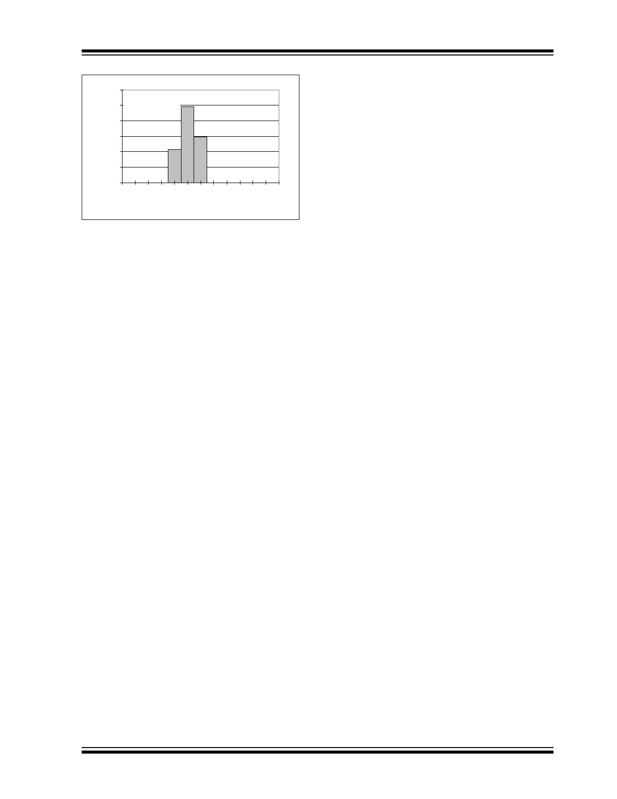
FIGURE 2-13:
Histogram of Temperature
Accuracy at +125 Degrees C (TC77-XXMXX).
0
10
20
30
40
50
60
-3 -2.5 -2 -1.5 -1 -0.5
0
0.5
1
1.5
2
2.5
3
Temperature Error (°C)
P
e
rcen
ta
g
e
o
f O
ccu
ra
n
ces (
%
)
Sample Size = 108
T
A
= +125°C
TC77
DS20092B-page 8
2002-2012 Microchip Technology Inc.
3.0
FUNCTIONAL DESCRIPTION
The TC77 consists of a band-gap type temperature
sensor, a 12-bit plus sign (13-bit) Sigma-Delta Analog-
to-Digital Converter (ADC), an internal conversion
oscillator (~30 kHz) and a serial input/output port.
These devices feature a three-wire serial interface that
is fully compatible with SPI and MICROWIRE specifica-
tions and, therefore, allows simple communications
with common microcontrollers and processors. The
Shutdown mode can be used to reduce supply current
for power sensitive applications. A Manufacturer’s ID
register identifies the TC77 as a Microchip Technology
product.
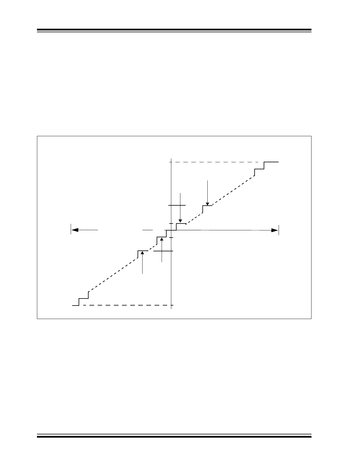
FIGURE 3-1:
Temperature To Digital Transfer Function (Non-linear Scale).
Temp
Temp
Output
Code
+125°C
-55°C
+25°C
-25°C
+0.0625°C
-0.0625°C
0+0111 1101 0000
0+0001 1001 0000
0+0000 0000 0001
0+0000 0000 0000
1+1111 1111 1111
1+1110 0111 0000
1+1100 1001 0000
0°C
2002-2012 Microchip Technology Inc.
DS20092B-page 9
TC77
3.1
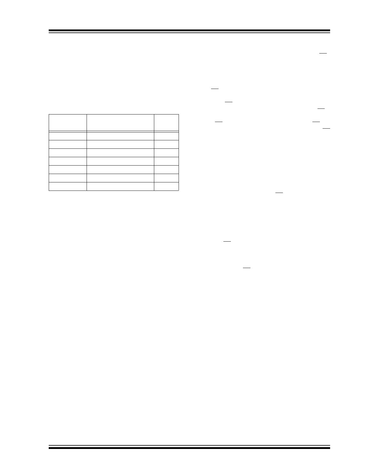
Temperature Data Format
A 13-bit two’s complement digital word is used to rep-
resent the temperature. The Least Significant Bit (LSb)
is equal to 0.0625°C. Note that the last two LSb bits (Bit
0 and 1) are tri-stated and are represented as a logic ‘1’
in the table. Bit 2 is set to logic ‘1’ after the completion
of the first temperature conversion following a power-
up or voltage reset event.
TABLE 3-1:
TC77 OUTPUT
An over-temperature condition can be determined by
reading only the first few Most Significant Bits (MSb) of
the temperature data. For example, the microprocessor
could read only the first four bits of the Temperature
register in order to determine that an over-temperature
condition exists.
3.2
Power-Up And Power-Down
The TC77 is in the Continuous Temperature Conver-
sion mode at power-up. The first valid temperature con-
version will be available approximately 300 ms (refer to
“Temperature to Bits Converter” section listed in the DC
characteristics table) after power-up. Bit 2 of the Tem-
perature register is set to a logic ‘1’ after the completion
of the first temperature conversion following a power-
up or voltage reset event. Bit 2 is set to logic ‘0’ during
the time needed to complete the first temperature con-
version. Thus, the status of bit 2 can be monitored to
indicate the completion of the first temperature conver-
sion.
A supply voltage lower than 1.6V (typ.) is considered a
power-down state for the TC77. The device will reset
itself and continue its normal Continuous Conversion
mode of operation when the supply voltage rises above
the nominal 1.6V. A minimal supply voltage of 2.7V is
required in order to ensure proper operation of the
device.
3.3
Serial Bus Interface
The serial interface consists of the Chip Select (CS),
Serial Clock (SCK) and Serial Data (SI/O) signals. The
TC77 meets the SPI and MICROWIRE bus specifica-
tions, with the serial interface designed to be compati-
ble with the Microchip PIC
®
family of microcontrollers.
The CS input is used to select the TC77 when multiple
devices are connected to the serial clock and data
lines. The CS line is also used to synchronize the data,
which is written to, or read from, the device when CS is
equal to a logic ‘0’ voltage. The SCK input is disabled
when CS is a logic ‘1’. The falling edge of the CS line
initiates communication, while the rising edge of CS
completes the communication.
The SCK input is provided by the external microcon-
troller and is used to synchronize the data on the SI/O
line. The Temperature and Manufacturer ID registers
are read only while the Configuration register is a read/
write register.
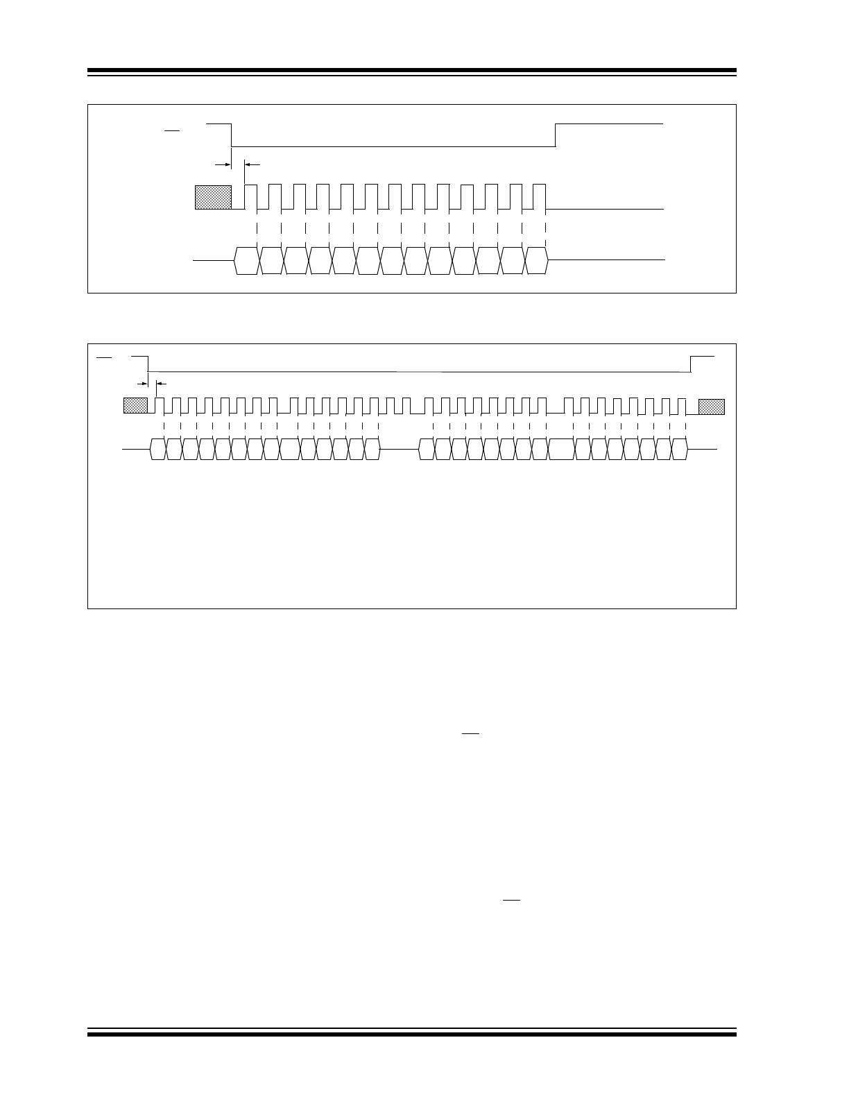
Figure 3-2 provides a timing diagram of a read opera-
tion of the Temperature register. Communication with
the TC77 is initiated when the CS goes to a logic ‘0’.
The Serial I/O signal (SI/O) then transmits the first bit of
data. The microcontroller serial I/O bus master clocks
the data in on the rising edge of SCK. The falling edge
of SCK is then used to clock out the rest of the data.
After 14 bits of data (thirteen temperature bits and Bit 2)
have been transmitted, the SI/O line is then tri-stated.
Note that CS can be taken to a logic ‘1’ at any time dur-
ing the data transmission if only a portion of the temper-
ature data information is required. The TC77 will
complete the conversion, and the output shift register
will be updated, if CS goes to the inactive state while in
the middle of a conversion.
Figure 3-3 provides a timing diagram of a multi-byte
communication operation consisting of a read of the
Temperature Data register, followed by a write to the
Configuration register. The first 16 SCK pulses are
used to transmit the TC77's temperature data to the
microcontroller. The second group of 16 SCK pulses
are used to receive the microcontroller command to
place the TC77 either in Shutdown or Continuous Tem-
perature Conversion mode. Note that the TC77 is in the
Continuous Temperature Conversion mode at power-
up.
The data written to the TC77’s Configuration register
should be either all 0’s or all 1’s, corresponding to
either the Continuous Temperature Conversion or
Shutdown mode, respectively. The TC77 is in Shut-
down mode when Bits C0 to C7 are all equal to 1’s. The
TC77 will be in the Continuous Conversion mode if a ‘0’
in any bit location from C0 to C7 is written to the
Configuration register.
Temperature
Binary
MSB / LSB
Hex
+125°C
0011 1110 1000 0111
3E 87h
+25°C
0000 1100 1000 0111
0B 87h
+0.0625°C
0000 0000 0000 1111
00 0Fh
0°C
0000 0000 0000 0111
00 07h
-0.0625°C
1111 1111 1111 1111
FF FFh
-25°C
1111 0011 1000 0111
F3 87h
-55°C
1110 0100 1000 0111
E4 87h
TC77
DS20092B-page 10
2002-2012 Microchip Technology Inc.
FIGURE 3-2:
Temperature Read Timing Diagram - (Reading only the first 13 Bits of the
Temperature Register).
FIGURE 3-3:
Temperature Read Followed By A Write To The Configuration Register Timing.
Diagram.
It is recommended that the user write all ‘0’s or all ‘1’s
to the Configuration register. While the following codes
can be transmitted to the TC77, any other code may
put the TC77 into a test mode reserved by Microchip for
calibration and production verification tests.
• 00 hex
• 01 hex
• 03 hex
• 07 hex
• 0F hex
• 1F hex
• 3F hex
• 7F hex
• FF hex
The following communication steps can be used to
obtain the Manufacturer's ID and put the device into the
Continuous Conversion mode. The Manufacturer’s ID
register is only accessible for a read operation, if the
TC77 is in Shutdown mode.
1.
CS goes low to initiate the communication cycle.
2.
Read 16 bits of temperature data from the
Temperature register.
3.
Write 16 bits of data (i.e. XXFF hex) to the Con-
figuration register to enter Shutdown mode.
4.
Read the 16 bits from the Manufacturer's ID reg-
ister (C15:C8 = 54 hex) to verify that the sensor
is a Microchip device.
5.
Write 8 to 16 bits of data (00 or 0000 hex) to
enter Continuous Conversion Mode.
6.
Return CS high to terminate the communication
cycle.
The time between a complete temperature conversion
and data transmission is approximately 300 msec.
CS
CLK
SI/O
t
CS-SCK
HI-Z
HI-Z
T
T
T
12
11
10
T
9
T
7
T
6
T
5
T
4
T
3
T
2
T
1
T
0
1
8
13
T
8
CS
CLK
SI/O
t
CS-SCK
HI-Z
1
8
8
8
8
1
HI-Z
1
1
HI-Z
TEMPERATURE REGISTER
Notes:
1.
Bit 2 = 0 during power-up for the first
temperature conversion.
2.
Bit 2 =1 after the completion of the first tem-
perature conversion following power-up or a
reset event.
3.
Bits 1 and 0 are “DON”T CARES”.
CONFIGURATION REGISTER
Notes:
1.
XX00 = Continuous Conversion Mode
2.
XXFF = Shutdown Mode
T
12
T
11
T
10
T
9
T
8
T
7
T
6
T
5
T
4
T
3
T
2
T
1
T
0
BIT
2
C
15
C
14
C
13
C
12
C
11
C
10
C
9
C
8
C
7
C
6
C
5
C
4
C
3
C
2
C
1
C
0
2002-2012 Microchip Technology Inc.
DS20092B-page 1
TC77
Features
• Digital Temperature Sensing in 5-Pin SOT-23A
and 8-Pin SOIC Packages
• Outputs Temperature as a 13-Bit Digital Word
• SPI and MICROWIRE™ Compatible Interface
• Solid State Temperature Sensing
• ±1°C (max.) accuracy from +25°C to +65°C
• ±2°C (max.) accuracy from -40°C to +85°C
• ±3°C (max.) accuracy from -55°C to +125°C
• 2.7V to 5.5V Operating Range
• Low Power
- 250 µA (typ.) Continuous Conversion Mode
- 0.1 µA (typ.) Shutdown Mode
Typical Applications
• Thermal Protection for Hard Disk Drives and
Other PC Peripherals
• PC Card Devices for Notebook Computers
• Low Cost Thermostat Controls
• Industrial Control
• Office Equipment
• Cellular Phones
• Thermistor Replacement
Block Diagram
Description
The TC77 is a serially accessible digital temperature
sensor particularly suited for low cost and small form-
factor applications. Temperature data is converted from
the internal thermal sensing element and made avail-
able at anytime as a 13-bit two’s compliment digital
word. Communication with the TC77 is accomplished
via a SPI and MICROWIRE compatible interface. It has
a 12-bit plus sign temperature resolution of 0.0625°C
per Least Significant Bit (LSb). The TC77 offers a tem-
perature accuracy of ±1.0°C (max.) over the tempera-
ture range of +25°C to +65°C. When operating, the
TC77 consumes only 250 µA (typ.). The TC77’s Con-
figuration register can be used to activate the low
power Shutdown mode, which has a current consump-
tion of only 0.1 µA (typ.). Small size, low cost and ease
of use make the TC77 an ideal choice for implementing
thermal management in a variety of systems.
Package Types
Typical Application
TC77
Diode
Temperature
Sensor
V
DD
SCK
CS
Serial
Port
Interface
SI/O
13-Bit
Sigma Delta
A/D Converter
Register
Temperature
Register
Internal
Configuration
Manufacturer
ID Register
V
SS
SOT-23-5
1
SOIC
1
V
DD
V
SS
SCK
SI/O
CS
TC77
TC77
SCK
SI/O
V
SS
NC
CS
V
DD
NC
NC
AN0
SCK
SDI
CS
SCK
SI/O
TC77
0.1µF
V
DD
V
SS
V
DD
PIC
®
MCU
Thermal Sensor with SPI Interfa
ce
TC77
DS20092B-page 2
2002-2012 Microchip Technology Inc.
1.0
ELECTRICAL
CHARACTERISTICS
1.1
Absolute Maximum Ratings †
V
DD
........................................................................6.0V
All inputs and outputs w.r.t. V
SS
..... -0.3V to V
DD
+0.3V
Storage temperature ..........................-65°C to +150°C
Ambient temp. with power applied .....-55°C to +125°C
Junction Temperature......................................... 150°C
ESD protection on all pins:
Human Body Model (HBM).............................. >4 kV
Machine Model (MM) ......................................>200V
† Notice: Stresses above those listed under "Maximum
Ratings" may cause permanent damage to the device. This is
a stress rating only and functional operation of the device at
those or any other conditions above those indicated in the
operation listings of this specification is not implied. Exposure
to maximum rating conditions for extended periods may affect
device reliability.
PIN FUNCTION TABLE
Name
Function
SI/O
Serial Data Pin
SCK
Serial Clock
V
SS
Ground
CS
Chip Select (Active-Low)
NC
No Connection
V
DD
Power Supply
DC CHARACTERISTICS
Electrical Specifications: Unless otherwise noted, all parameters apply at V
DD
= 2.7V to 5.5V and
T
A
= -55°C to +125°C.
Parameters
Sym
Min
Typ
Max
Units
Conditions
Power Supply
Operating Voltage Range
V
DD
2.7
—
5.5
V
Note 1
Operating Current
I
DD
—
250
400
µA
Continuous Temperature
Conversion Mode
Power-On Reset Threshold
V
POR
1.2
1.6
2.2
V
V
DD
falling or rising edge
Standby Supply Current
I
DD-
STANDBY
—
0.1
1.0
µA
Shutdown Mode
Temperature to Bits Converter
Resolution
—
13
—
Bits
ADC LSb = 0.0625°C/bit
(Note 4)
Temperature Conversion Time
t
CT
—
300
400
ms
Temperature Accuracy
(Note 1)
T
ERR
-1.0
-2.0
-3.0
—
—
—
+1.0
+2.0
+3.0
°C
+25°C < T
A
< +65°C
-40°C < T
A
< +85°C
-55°C < T
A
< +125°C
TC77-3.3MXX: V
DD
= 3.3V
TC77-5.0MXX: V
DD
= 5.0V
Note 1: The TC77-3.3MXX and TC77-5.0MXX will operate from a supply voltage of 2.7V to 5.5V. However, the tem-
perature accuracy of the TC77-3.3MXX and TC77-5.0MXX is specified at the nominal operating voltages of
3.3V and 5.0V, respectively. As V
DD
varies from the nominal operating value, the accuracy may be
degraded (Refer to Figures 2-6 and 2-7).
2: All time measurements are measured with respect to the 50% point of the signal.
3: Load Capacitance, C
L
= 80 pF, is used for AC timing measurements of output signals.
4: Resolution = Temperature Range/No. of Bits = (+255°C – -256°C) / (2
13
)
Resolution = 512/8192 = 0.0625°C/Bit
2002-2012 Microchip Technology Inc.
DS20092B-page 3
TC77
Digital Input/Output
High Level Input Voltage
V
IH
0.7 V
DD
—
V
DD
+ 0.3
V
Low Level Input Voltage
V
IL
-0.3
—
0.3 V
DD
V
High Level Output Voltage
V
OH
2.4
—
—
V
I
OH
= -400 µA
Low Level Output Voltage
V
OL
—
—
0.4
V
I
OL
= +2 mA
Input Current
I
IN(0),
I
IN(1)
-1.0
-1.0
—
—
+1.0
+1.0
µA
V
IN
= GND
V
IN
= V
DD
Input Hysteresis
0.35
0.8
—
V
SI/O, SCK
Pin Capacitance
C
IN
, C
OUT
—
20
—
pF
Tri-state Output Leakage
Current
I
O_LEAK
-1.0
—
—
—
—
+1.0
µA
V
O
= GND
V
O
= V
DD
Serial Port AC Timing (Notes 2, 3)
Clock Frequency
f
CLK
DC
—
7.0
MHz
CS Fall to First Rising SCK
Edge
t
CS-SCK
100
—
—
ns
CS Low to Data Out Delay
t
CS-SI/O
—
—
70
ns
SCK Fall to Data Out Delay
t
DO
—
—
100
ns
CS High to Data Out
Tri-state
t
DIS
—
—
200
ns
SCK High to Data In Hold Time
t
HD
50
—
—
ns
Data In Set-up Time
t
SU
30
—
—
ns
Thermal Package Resistance
Thermal Resistance, SOT23-5
JA
—
230
—
°C/W
Thermal Resistance, 8L-SOIC
JA
—
163
—
°C/W
DC CHARACTERISTICS (CONTINUED)
Electrical Specifications: Unless otherwise noted, all parameters apply at V
DD
= 2.7V to 5.5V and
T
A
= -55°C to +125°C.
Parameters
Sym
Min
Typ
Max
Units
Conditions
Note 1: The TC77-3.3MXX and TC77-5.0MXX will operate from a supply voltage of 2.7V to 5.5V. However, the tem-
perature accuracy of the TC77-3.3MXX and TC77-5.0MXX is specified at the nominal operating voltages of
3.3V and 5.0V, respectively. As V
DD
varies from the nominal operating value, the accuracy may be
degraded (Refer to Figures 2-6 and 2-7).
2: All time measurements are measured with respect to the 50% point of the signal.
3: Load Capacitance, C
L
= 80 pF, is used for AC timing measurements of output signals.
4: Resolution = Temperature Range/No. of Bits = (+255°C – -256°C) / (2
13
)
Resolution = 512/8192 = 0.0625°C/Bit
TC77
DS20092B-page 4
2002-2012 Microchip Technology Inc.
FIGURE 1-1:
Timing Diagrams.
CS
SCK
1/f
CLK
SI/O
t
DO
LSb
t
DIS
HI-Z
Data Output Timing
MSb
t
CS-SI/O
t
HD
t
SU
SI/O
SCK
CS
HI-Z
SI/O
SCK
CS
HI-Z
t
HD
t
SU
HI-Z
t
CS-SCK
SI/O Data Input Set-up and Hold Timing (Data is clocked on the rising edge of SCK)
2002-2012 Microchip Technology Inc.
DS20092B-page 5
TC77
2.0
TYPICAL PERFORMANCE CURVES
Note: Unless otherwise indicated, all parameters apply at V
DD
= 3.3V for the TC77-3.3MXX and V
DD
= 5.0V for the TC77-
5.0MXX, and T
A
= -55°C to +125°C. The TC77-3.3MXX and TC77-5.0MXX will operate from a supply voltage of 2.7V
to 5.5V. However, the temperature accuracy of the TC77-3.3MXX and TC77-5.0MXX is specified at the nominal oper-
ating voltages of 3.3V and 5.0V, respectively.
FIGURE 2-1:
Accuracy vs. Temperature
(TC77-XXMXX)
.
FIGURE 2-2:
Supply Current vs. Supply
Voltage (TC77-XXMXX).
FIGURE 2-3:
Supply Current vs.
Temperature.
FIGURE 2-4:
Shutdown Current vs.
Temperature.
FIGURE 2-5:
Power-On Reset Voltage vs.
Temperature (TC77-XXMXX).
FIGURE 2-6:
Temperature Accuracy vs.
Supply Voltage (TC77-3.3MXX).
Note:
The graphs and tables provided following this note are a statistical summary based on a limited number of
samples and are provided for informational purposes only. The performance characteristics listed herein
are not tested or guaranteed. In some graphs or tables, the data presented may be outside the specified
operating range (e.g., outside specified power supply range) and therefore outside the warranted range.
-3.5
-3
-2.5
-2
-1.5
-1
-0.5
0
0.5
1
1.5
2
2.5
3
3.5
-55 -35 -15
5
25
45
65
85 105 125
Reference Temperature (°C)
Temperature Error (°C)
Upper Specification Limit
Lower Specification Limit
Mean + 3V
Mean - 3V
Mean
200
210
220
230
240
250
2.7
3.1
3.5
3.9
4.3
4.7
5.1
5.5
Supply Voltage (V)
Suppl
y Cur
re
nt
(
µ
A)
T
A
= +25°C
T
A
= +125°C
T
A
= -55°C
0
50
100
150
200
250
300
350
400
-55
-25
5
35
65
95
125
Temperature (°C)
Suppl
y Cur
re
nt
(
µ
A)
TC77-5.0MXX
V
DD
= 5.0 V
TC77-3.3MXX
V
DD
= 3.3 V
0.0
0.1
0.2
0.3
-55
-25
5
35
65
95
125
Temperature (°C)
Shut
dow
n Cur
re
nt
(
µ
A)
TC77-5.0MXX
V
DD
= 5.0 V
TC77-3.3MXX
V
DD
= 3.3 V
0.0
0.5
1.0
1.5
2.0
2.5
-55
-25
5
35
65
95
125
Temperature (°C)
Pow
e
r-
O
n
R
eset
Vol
tage (
V
)
-0.4
-0.3
-0.2
-0.1
0
0.1
0.2
0.3
0.4
3
3.1
3.2
3.3
3.4
3.5
3.6
Supply Voltage (V)
Tem
p
er
at
ur
e C
h
ange (
°C
)
TC77-3.3MXX
T
A
= -25°C
T
A
= +25°C
T
A
= +85°C
TC77
DS20092B-page 6
2002-2012 Microchip Technology Inc.
FIGURE 2-7:
Temperature Accuracy vs.
Supply Voltage (TC77-5.0MXX).
FIGURE 2-8:
Histogram of Temperature
Accuracy at -55 Degrees C (TC77-XXMXX).
FIGURE 2-9:
Histogram of Temperature
Accuracy at -40 Degrees C (TC77-XXMXX).
FIGURE 2-10:
Histogram of Temperature
Accuracy at +25 Degrees C (TC77-XXMXX).
FIGURE 2-11:
Histogram of Temperature
Accuracy at +65 Degrees C (TC77-XXMXX).
FIGURE 2-12:
Histogram of Temperature
Accuracy at +85 Degrees C (TC77-XXMXX).
-0.4
-0.3
-0.2
-0.1
0
0.1
0.2
0.3
0.4
4.5 4.6 4.7 4.8 4.9
5
5.1 5.2 5.3 5.4 5.5
Supply Voltage (V)
Tem
p
er
at
ur
e C
h
ange (
°C
)
TC77-5.0MXX
T
A
= -25°C
T
A
= +25°C
T
A
= +85°C
0
5
10
15
20
25
30
35
-3 -2.5 -2 -1.5 -1 -0.5
0
0.5
1
1.5
2
2.5
3
Temperature Error (°C)
P
e
rcen
ta
g
e
o
f O
ccu
ra
n
ces (
%
)
Sample Size = 108
T
A
= -55°C
0
5
10
15
20
25
30
35
40
-2
-1.5
-1
-0.5
0
0.5
1
1.5
2
Temperature Error (°C)
P
e
rcen
ta
g
e
o
f O
ccu
ra
n
ces (
%
)
Sample Size = 108
T
A
= -40°C
0
5
10
15
20
25
30
35
40
45
50
-1
-0.75
-0.5
-0.25
0
0.25
0.5
0.75
1
Temperature Error (°C)
P
e
rcen
ta
g
e
o
f O
ccu
ra
n
ces (
%
)
Sample Size = 108
T
A
= +25°C
0
5
10
15
20
25
30
35
40
45
50
-1
-0.75
-0.5
-0.25
0
0.25
0.5
0.75
1
Temperature Error (°C)
P
e
rcen
ta
g
e
o
f O
ccu
ra
n
ces (
%
)
Sample Size = 108
T
A
= +65°C
0
10
20
30
40
50
60
70
80
90
-2
-1.5
-1
-0.5
0
0.5
1
1.5
2
Temperature Error (°C)
P
e
rcen
ta
g
e
o
f O
ccu
ra
n
ces (
%
)
Sample Size = 108
T
A
= +85°C
2002-2012 Microchip Technology Inc.
DS20092B-page 7
TC77
FIGURE 2-13:
Histogram of Temperature
Accuracy at +125 Degrees C (TC77-XXMXX).
0
10
20
30
40
50
60
-3 -2.5 -2 -1.5 -1 -0.5
0
0.5
1
1.5
2
2.5
3
Temperature Error (°C)
P
e
rcen
ta
g
e
o
f O
ccu
ra
n
ces (
%
)
Sample Size = 108
T
A
= +125°C
TC77
DS20092B-page 8
2002-2012 Microchip Technology Inc.
3.0
FUNCTIONAL DESCRIPTION
The TC77 consists of a band-gap type temperature
sensor, a 12-bit plus sign (13-bit) Sigma-Delta Analog-
to-Digital Converter (ADC), an internal conversion
oscillator (~30 kHz) and a serial input/output port.
These devices feature a three-wire serial interface that
is fully compatible with SPI and MICROWIRE specifica-
tions and, therefore, allows simple communications
with common microcontrollers and processors. The
Shutdown mode can be used to reduce supply current
for power sensitive applications. A Manufacturer’s ID
register identifies the TC77 as a Microchip Technology
product.
FIGURE 3-1:
Temperature To Digital Transfer Function (Non-linear Scale).
Temp
Temp
Output
Code
+125°C
-55°C
+25°C
-25°C
+0.0625°C
-0.0625°C
0+0111 1101 0000
0+0001 1001 0000
0+0000 0000 0001
0+0000 0000 0000
1+1111 1111 1111
1+1110 0111 0000
1+1100 1001 0000
0°C
2002-2012 Microchip Technology Inc.
DS20092B-page 9
TC77
3.1
Temperature Data Format
A 13-bit two’s complement digital word is used to rep-
resent the temperature. The Least Significant Bit (LSb)
is equal to 0.0625°C. Note that the last two LSb bits (Bit
0 and 1) are tri-stated and are represented as a logic ‘1’
in the table. Bit 2 is set to logic ‘1’ after the completion
of the first temperature conversion following a power-
up or voltage reset event.
TABLE 3-1:
TC77 OUTPUT
An over-temperature condition can be determined by
reading only the first few Most Significant Bits (MSb) of
the temperature data. For example, the microprocessor
could read only the first four bits of the Temperature
register in order to determine that an over-temperature
condition exists.
3.2
Power-Up And Power-Down
The TC77 is in the Continuous Temperature Conver-
sion mode at power-up. The first valid temperature con-
version will be available approximately 300 ms (refer to
“Temperature to Bits Converter” section listed in the DC
characteristics table) after power-up. Bit 2 of the Tem-
perature register is set to a logic ‘1’ after the completion
of the first temperature conversion following a power-
up or voltage reset event. Bit 2 is set to logic ‘0’ during
the time needed to complete the first temperature con-
version. Thus, the status of bit 2 can be monitored to
indicate the completion of the first temperature conver-
sion.
A supply voltage lower than 1.6V (typ.) is considered a
power-down state for the TC77. The device will reset
itself and continue its normal Continuous Conversion
mode of operation when the supply voltage rises above
the nominal 1.6V. A minimal supply voltage of 2.7V is
required in order to ensure proper operation of the
device.
3.3
Serial Bus Interface
The serial interface consists of the Chip Select (CS),
Serial Clock (SCK) and Serial Data (SI/O) signals. The
TC77 meets the SPI and MICROWIRE bus specifica-
tions, with the serial interface designed to be compati-
ble with the Microchip PIC
®
family of microcontrollers.
The CS input is used to select the TC77 when multiple
devices are connected to the serial clock and data
lines. The CS line is also used to synchronize the data,
which is written to, or read from, the device when CS is
equal to a logic ‘0’ voltage. The SCK input is disabled
when CS is a logic ‘1’. The falling edge of the CS line
initiates communication, while the rising edge of CS
completes the communication.
The SCK input is provided by the external microcon-
troller and is used to synchronize the data on the SI/O
line. The Temperature and Manufacturer ID registers
are read only while the Configuration register is a read/
write register.
Figure 3-2 provides a timing diagram of a read opera-
tion of the Temperature register. Communication with
the TC77 is initiated when the CS goes to a logic ‘0’.
The Serial I/O signal (SI/O) then transmits the first bit of
data. The microcontroller serial I/O bus master clocks
the data in on the rising edge of SCK. The falling edge
of SCK is then used to clock out the rest of the data.
After 14 bits of data (thirteen temperature bits and Bit 2)
have been transmitted, the SI/O line is then tri-stated.
Note that CS can be taken to a logic ‘1’ at any time dur-
ing the data transmission if only a portion of the temper-
ature data information is required. The TC77 will
complete the conversion, and the output shift register
will be updated, if CS goes to the inactive state while in
the middle of a conversion.
Figure 3-3 provides a timing diagram of a multi-byte
communication operation consisting of a read of the
Temperature Data register, followed by a write to the
Configuration register. The first 16 SCK pulses are
used to transmit the TC77's temperature data to the
microcontroller. The second group of 16 SCK pulses
are used to receive the microcontroller command to
place the TC77 either in Shutdown or Continuous Tem-
perature Conversion mode. Note that the TC77 is in the
Continuous Temperature Conversion mode at power-
up.
The data written to the TC77’s Configuration register
should be either all 0’s or all 1’s, corresponding to
either the Continuous Temperature Conversion or
Shutdown mode, respectively. The TC77 is in Shut-
down mode when Bits C0 to C7 are all equal to 1’s. The
TC77 will be in the Continuous Conversion mode if a ‘0’
in any bit location from C0 to C7 is written to the
Configuration register.
Temperature
Binary
MSB / LSB
Hex
+125°C
0011 1110 1000 0111
3E 87h
+25°C
0000 1100 1000 0111
0B 87h
+0.0625°C
0000 0000 0000 1111
00 0Fh
0°C
0000 0000 0000 0111
00 07h
-0.0625°C
1111 1111 1111 1111
FF FFh
-25°C
1111 0011 1000 0111
F3 87h
-55°C
1110 0100 1000 0111
E4 87h
TC77
DS20092B-page 10
2002-2012 Microchip Technology Inc.
FIGURE 3-2:
Temperature Read Timing Diagram - (Reading only the first 13 Bits of the
Temperature Register).
FIGURE 3-3:
Temperature Read Followed By A Write To The Configuration Register Timing.
Diagram.
It is recommended that the user write all ‘0’s or all ‘1’s
to the Configuration register. While the following codes
can be transmitted to the TC77, any other code may
put the TC77 into a test mode reserved by Microchip for
calibration and production verification tests.
• 00 hex
• 01 hex
• 03 hex
• 07 hex
• 0F hex
• 1F hex
• 3F hex
• 7F hex
• FF hex
The following communication steps can be used to
obtain the Manufacturer's ID and put the device into the
Continuous Conversion mode. The Manufacturer’s ID
register is only accessible for a read operation, if the
TC77 is in Shutdown mode.
1.
CS goes low to initiate the communication cycle.
2.
Read 16 bits of temperature data from the
Temperature register.
3.
Write 16 bits of data (i.e. XXFF hex) to the Con-
figuration register to enter Shutdown mode.
4.
Read the 16 bits from the Manufacturer's ID reg-
ister (C15:C8 = 54 hex) to verify that the sensor
is a Microchip device.
5.
Write 8 to 16 bits of data (00 or 0000 hex) to
enter Continuous Conversion Mode.
6.
Return CS high to terminate the communication
cycle.
The time between a complete temperature conversion
and data transmission is approximately 300 msec.
CS
CLK
SI/O
t
CS-SCK
HI-Z
HI-Z
T
T
T
12
11
10
T
9
T
7
T
6
T
5
T
4
T
3
T
2
T
1
T
0
1
8
13
T
8
CS
CLK
SI/O
t
CS-SCK
HI-Z
1
8
8
8
8
1
HI-Z
1
1
HI-Z
TEMPERATURE REGISTER
Notes:
1.
Bit 2 = 0 during power-up for the first
temperature conversion.
2.
Bit 2 =1 after the completion of the first tem-
perature conversion following power-up or a
reset event.
3.
Bits 1 and 0 are “DON”T CARES”.
CONFIGURATION REGISTER
Notes:
1.
XX00 = Continuous Conversion Mode
2.
XXFF = Shutdown Mode
T
12
T
11
T
10
T
9
T
8
T
7
T
6
T
5
T
4
T
3
T
2
T
1
T
0
BIT
2
C
15
C
14
C
13
C
12
C
11
C
10
C
9
C
8
C
7
C
6
C
5
C
4
C
3
C
2
C
1
C
0