
2002-2012 Microchip Technology Inc.
DS20091C-page 1
MCP18480
Features
• Allows safe board removal and insertion from a
live backplane
• Accurate (<1.5%) internal voltage reference for
fault detection and precision timing
• Programmable foldback current limiting
• Programmable circuit breaker current limiting
• Auto restart option for all faults
• Adjustable Undervoltage lockout thresholds
• Adjustable Overvoltage protection threshold
• Adjustable Power Good delay
• Configurable Power Good output polarity
• Low-side drive of an external N-channel FET
CMOS Technology
• High-Voltage Operation
• Temperature range: Industrial (I): -40°C to +85°C
Packaging
• 20-lead SSOP
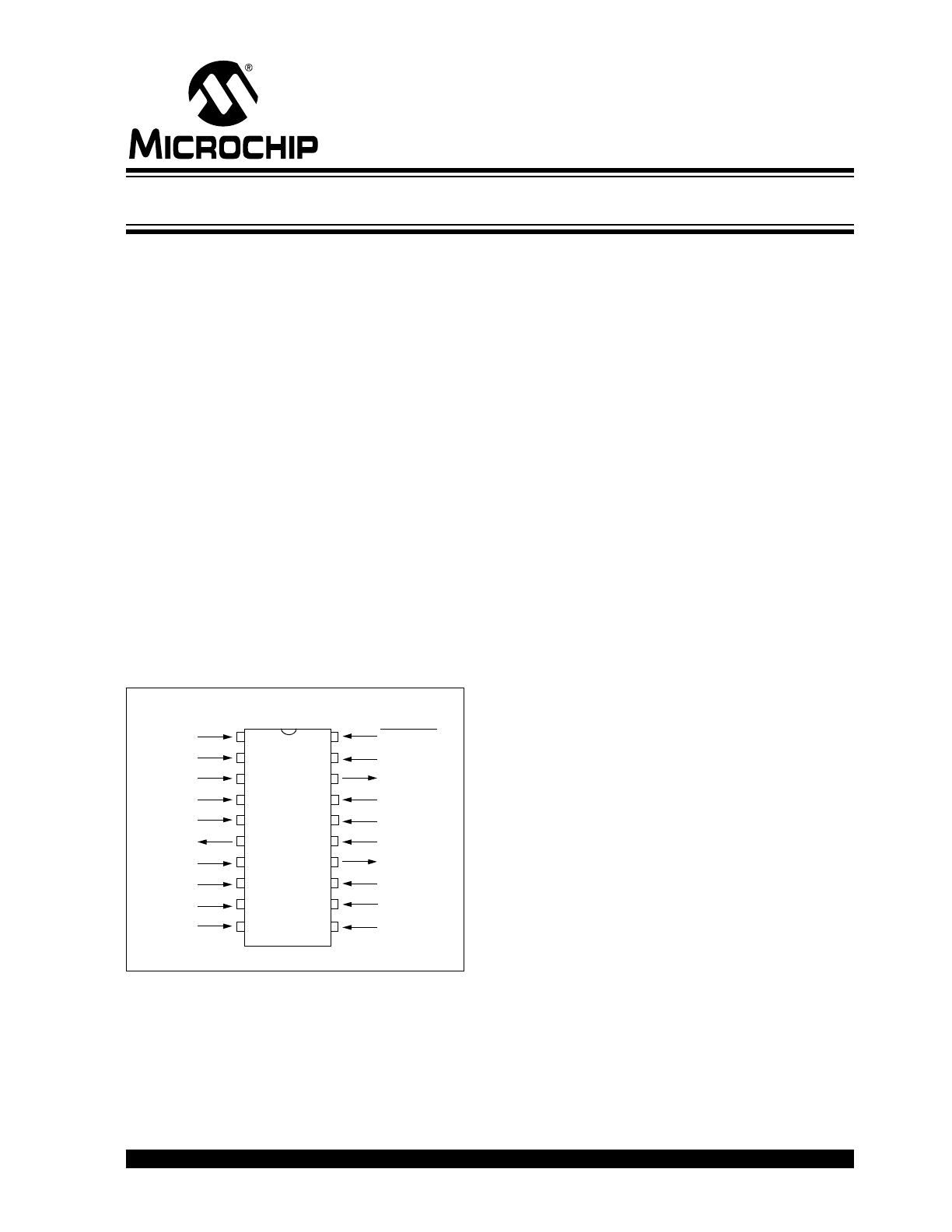
Package Type
Description
The MCP18480 is a Hot Swap controller that allows
boards to be safely removed or inserted from an active
backplane using -48V.
When PCBs are inserted into a live backplane, high-
peak or transient currents from the source are gener-
ated due to the charging of the bypass capacitors on
the supply. The high transient currents can destroy
connectors and capacitors. The high inrush current can
pull the input voltage BUS down and reset the system.
The MCP18480 solves this problem by controlling the
slew rate of the backplane voltage to the board so that
these transients are eliminated. This allows boards to
be removed and inserted without causing damage to
connector pins and input bulk capacitors, in addition to
preventing false resets to the other boards on the
backplane.
The MCP18480 can be used in applications in several
areas including:
• Telecom Line Cards
• Network Switches
• Network Routers and Servers
• Base Station Line Cards
• Power-Over-LAN
• Power-Over-MDI
• IP Phone Switches/Routers
• Mid-Span, Power-Over-MDI
Two forms of current limit are provided in the
MCP18480. These are:
• Foldback
• Circuit breaker
The foldback current-limiting circuit uses an external
sense resistor and a voltage that is proportional to the
external MOSFET’s drain voltage. These are used to
keep the MOSFET in its Safe Operating Area (SOA).
If the device remains in current limit for a programmed
time period, the external N-channel FET is turned off.
The option exists to configure the device to automati-
cally restart after a programmed time delay. A program-
mable catastrophic current limit threshold shuts down
the switch (circuit breaker) if excessive current is
sensed due to a short-circuit condition.
2
3
4
5
6
7
8
9
10
1
19
18
16
15
14
13
12
11
17
20
ENABLE
RESTART
UV
D
V
REFIN
OVO
V
FB
PWRGOOD
DRAIN
TH
SENSE
GATE
CL
I
SET
TIMER
R
DISCH
V
NEG
OV
TH
UV
TH
UV
HYS
V
REFOUT
V
POS
MCP
184
80
SSOP
-48V Hot Swap Controller
MCP18480
DS20091C-page 2
2002-2012 Microchip Technology Inc.
Internal comparators are incorporated to add hystere-
sis for adjusting the Undervoltage Lockout (UVLO)
threshold. The external N-channel MOSFET is turned
on when the input is below the user-programmable,
Overvoltage threshold and above the user-
programmable, Undervoltage threshold.
The PWRGOOD pin indicates the status of the
MCP18480 and is active when the device has com-
pleted power-up and the system is not in an Undervolt-
age, Overvoltage or current-limit condition.
PWRGOOD can be externally configured to either
active-high or active-low to accommodate external cir-
cuitry (power supplies) that have either enabling logic.
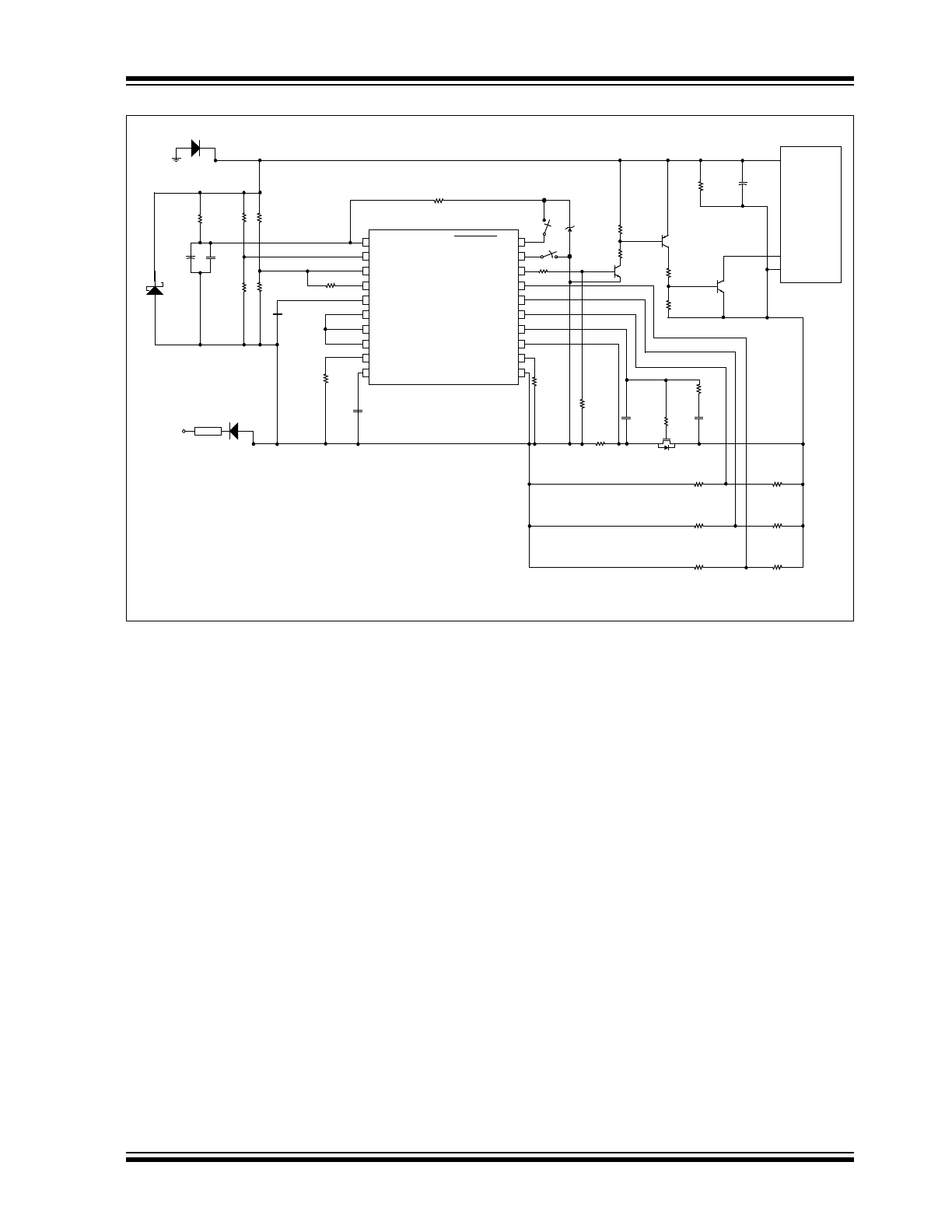
A block diagram of the MCP18480 is shown below.
MCP18480 Block Diagram
V
POS
UV
TH
UV
D
OV
TH
V
NEG
GATE
V
FB
MCP18480
UV
HYS
V
REFOUT
V
REFIN
SENSE
TIMER
R
DISCH
LA
T
CHOF
F
I
SET
PWRGOOD
(1)
DRAIN
TH
12V
Regulator
12V
OUT
5V
Reg.
5V
OUT
5V
OUT
Latch
Undervolt
age A
c
ti
ve
O
v
erv
o
lt
age Act
ive
Current Limit Timer
ENABLE
RESTART
CL
V
POS
OVO
PWRGOOD
Output Block
V
NEG
BIAS
Undervoltage
Overvoltage
Current Limit
GATE
Drive
Timer
FET Good
Circuit Breaker
TIM
E
O
U
T
Cu
rrent
Limit
F
eedback
SENSE
Internal
Bias
Generation
Note 1:
The PWRGOOD output pin can be either active-high or active-low. This polarity is determined by the
voltage (either the level on the V
REFIN
pin or level on the
V
NEG
pin) on the I
SET
pin:
-
Connecting the external
R
ISET
resistor to V
REFIN
configures the PWRGOOD pin as active-low
-
Connecting the external
R
ISET
resistor to
V
NEG
configures the PWRGOOD pin as active-high
(Section 6.8.3)
(Section 6.8.8)
(Section 6.8.2)
(Section 6.8.1)
(Section 6.8.4)
(Section 6.8.9)
(Section 6.8.5)
(Section
6.8.6)
(Section 6.8.7)
2002-2012 Microchip Technology Inc.
DS20091C-page 3
MCP18480
1.0
ELECTRICAL
CHARACTERISTICS
Absolute Maximum Ratings†
Ambient Temperature under bias ........ –40°C to +85°C
Storage Temperature ........................ –65°C to +150°C
Voltage on V
POS
with respect to V
NEG
-0.3V to +15.0V
Voltage on DV
TH
, UV
TH
, V
FB
, OVO and UV
HYS
pins
with respect to V
NEG
..... V
NEG
– 0.3V to (V
POS
+ 0.3V)
Voltage on V
REFIN
, CL, SENSE, DRAIN
TH
, ENABLE
and RESTART pins with respect to V
NEG
........................................................ V
NEG
- 0.3V to 6V.
Total Power Dissipation (Note 1) .................... 800 mW
Max. Current out of V
NEG
pin ............................. 80 mA
Max. Current into V
POS
pin ................................ 50 mA
Max. Output Current sunk by Gate pin............... 80 mA
Max. Output Current sunk by V
REFOUT
pin .......... 5 mA
Max. Output Current sunk by any other
Output pin......................................................... 25 mA
Max. Output Current sourced by Gate pin ........ 200 µA
Max. Output Current sourced by V
REFOUT
pin ..... 5 mA
Max. Output Current sourced by any other
Output pin........................................................... 25 mA
Junction to Ambient,
JA
(20 pin SSOP Package) Derating ...............108.1
C/W
Junction to Case,
JC
(20 pin SSOP Package) Derating .................32.2
C/W
Lead Temperature, Soldering, 10 seconds ........ 300
C
† Notice: Stresses above those listed under "Maximum
Ratings" may cause permanent damage to the device. This is
a stress rating only and functional operation of the device at
those or any other conditions above those indicated in the
operation listings of this specification is not implied. Exposure
to maximum rating conditions for extended periods may affect
device reliability.
Note 1: Power Dissipation is calculated as follows:
P
DIS
= V
DD
x {I
DD
-
I
OH
} +
{(V
DD
-V
OH
) x I
OH
} +
(V
OL
x I
OL
)
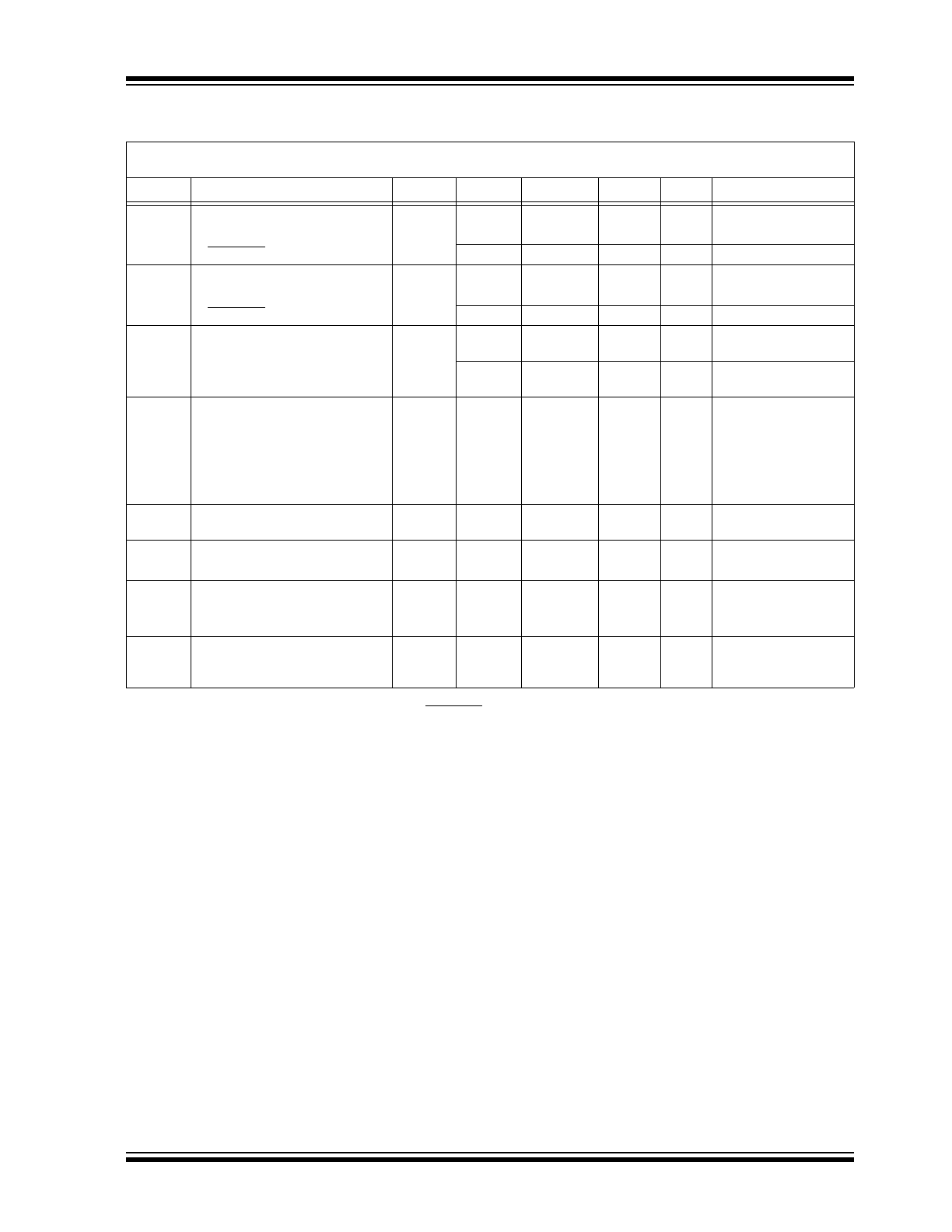
DC CHARACTERISTICS
Electrical Specifications: Unless otherwise specified, operating temperature: –40
C T
A
+85C (Industrial),
Supply Current: 5 mA
I
POS
25 mA, R
ISET
= 125 k
, C
BYP
= 2 µF.
Param.
No.
Parameter
Sym
Min
Typ
(1)
Max
Units
Conditions
MD001
Current into shunt regulator
that produces V
POS
output volt-
age that meets MD001A speci-
fication
I
POS1
5
—
25
mA
ENABLE pin = 5V
5
—
25
ENABLE pin = V
NEG
MD001A
Regulated Output Voltage
Differential of V
POS
to V
NEG
V
POS
10.4
12.0
13.4
V
See MD001
MD002
V
REFOUT
pin output voltage
V
REFOUT
2.463
2.5
2.538
V
Load = 50 µA
MD010
V
GATE
pin output voltage
V
GATE
V
POS
- 2
V
POS
-1
V
POS
V
MD011
Voltage on I
SET
pin
V
ISET
(V
REFIN
/2) -
0.02
V
REFIN
/2
(V
REFIN
/2)
+0.02
V
MD012A
Voltage on SENSE pin to
trigger current-limiting
V
SENSE
40
50
60
mV
V
FB
= V
NEG
MD012B
25
31.0
40
mV
V
FB
= V
NEG
+ 0.25V
MD012C
7
12
17
mV
V
FB
= V
NEG
+ 0.5V
MD013
Undervoltage Threshold
UV
TH
V
REFIN
- 0.03
V
REFIN
V
REFIN
+ 0.03
V
MD014A
Overvoltage
Threshold
rising
OV
TH
V
REFIN
- 0.05
V
REFIN
V
REFIN
+ 0.05
V
V
REFIN
= 2.5V
MD014B
falling
OV
TH
V
REFIN
- 0.035
V
REFIN
- 0.02
V
REFIN
- 0.005
V
V
REFIN
= 2.5V
MD015
DRAIN Pin Input Threshold
Voltage
V
DTH
90
100
130
mV
Note
1: Data in the Typical (“Typ”) column is based on characterization results at +25
C. This data is for design guidance only
and is not tested.
2: Negative current is defined as current sourced by the pin.
3: All voltages are with respect to the V
NEG
pin voltage.
MCP18480
DS20091C-page 4
2002-2012 Microchip Technology Inc.
DC Characteristics (Continued)
Electrical Specification: Unless otherwise specified, operating temperature: –40
C T
A
+85C (Industrial),
Supply Current: 5 mA
I
POS
25 mA, R
ISET
= 125 k
C
BYP
= 2 µF
Param.
No.
Parameter
Sym
Min
Typ
(1)
Max
Units
Conditions
MD020
DRAIN pin current
I
DRAIN
—
—
0.1
µA
DRAIN
TH
pin = V
NEG
MD021
SENSE pin current
I
SENSE
—
—
0.1
µA
MD022
GATE pin current
Pull-up
I
GATE
SENSE pin = V
NEG
GATE pin = V
NEG
+4V
MD022A
-30
-50
-75
µA
V
FB
= V
NEG
MD022B
-9
-17
-33
µA
V
FB
= V
NEG
+ 500 mV
MD022C
Pull-down
I
GATE
31
49
72
mA
Any fault condition
MD023
UV
D
pin current
I
UVD
-7
-10
-15
µA
UV
TH
< V
REFIN
MD024A
TIMER pin current
Pull-up
I
TIMER
-100
-160
-200
µA
R
ISET
= 125 k
,
V
REFIN
= 2.5V
MD024B
Pull-down
52
78
104
nA
R
ISET
= 125 k
,
V
REFIN
= 2.5V
R
DISCH
= 1.6 M
MD025
I
SET
pin current
I
ISET
V
ISET(MIN)
—
V
ISET(MAX)
A
See MD011
R
ISET(MAX)
R
ISET(MIN)
Note
1: Data in the Typical (“Typ”) column is based on characterization results at +25
C. This data is for design guidance only
and is not tested.
2: Negative current is defined as current sourced by the pin.
3: All voltages are with respect to the V
NEG
pin voltage.
2002-2012 Microchip Technology Inc.
DS20091C-page 5
MCP18480
DC Characteristics (Continued)
Electrical Specifications: Unless otherwise specified, operating temperature: –40
C T
A
+85C (Industrial),
Supply Current: 5 mA
I
POS
25 mA, R
ISET
= 125 k
, C
BYP
= 2 µF.
Param #
Parameter
Sym
Min
Typ
Max
Units
Conditions
MD030
Input Low Voltage
V
IL
MD031
ENABLE pin
V
NEG
—
0.8
V
MD032
RESTART pin
V
NEG
—
0.8
MD040
Input High Voltage
V
IH
MD041
ENABLE pin
2.0
—
5.0
V
MD042
RESTART pin
2.0
—
5.0
V
MD050
Internal Resistance on UV
HYS
pin
R
UVHYS
500
1200
2100
V
UVTH
< V
REFIN
,
I
UVHYS
= 30 µA
50
100
—
M
V
UVTH
> V
REFIN
,
I
UVHYS
= 30 µA
Input Leakage Current
(
Notes 2
,
3
)
MD060A
OV
TH
, UV
TH
, V
FB
, OVO and UV
HYS
pins
I
IL
-1
—
+1
µA
V
NEG
V
PIN
11V, Pin
at high-impedance
MD060B
V
REFIN
, CL, SENSE, DRAIN
TH
,
ENABLE and RESTART pins
—
—
±1
µA
V
NEG
V
PIN
5V,
Pin at hi-impedance
MD070
Minimum current into ENABLE pin
to disable MCP18480
I
EN
—
10
30
µA
I
POS
= 5 mA,
ENABLE = 0.8V
Output Low Voltage
V
OL
MD080
PWRGOOD pin
0
—
0.4
V
I
OL
= 5 mA
Output High Voltage
V
OH
—
MD090
PWRGOOD pin
0.8 V
POS
0.96 V
POS
V
POS
V
I
OH
= 2 mA,
7 mA
I
POS
12 mA
MD100
Offset Voltage at the internal
comparator input that is connected
to the CL pin.
V
CL
-15
—
+15
mV
V
FB
= 0
Note
1: All voltages are with respect to the V
NEG
pin voltage.
2: The leakage currents on the ENABLE and RESTART pins are strongly dependent on the applied voltage level. The spec-
ified levels represent normal operating conditions. Higher leakage current may be measured at different input voltages.
3: Negative current is defined as coming out of the pin.
MCP18480
DS20091C-page 6
2002-2012 Microchip Technology Inc.
1.1
Timing Parameter Symbology and Load Conditions
The timing parameter symbols have been created using one of the following formats:
1.1.1
TIMING CONDITIONS
The temperature and voltages specified in
Table 1-2
apply to all timing specifications, unless otherwise noted.
Figure 1-1
specifies the load conditions for the timing specifications.
TABLE 1-1:
SYMBOLOGY
TABLE 1-2:
AC TEMPERATURE AND VOLTAGE SPECIFICATIONS
1. TppS2ppS
2. TppS
T
F
Frequency
T
Time
E
Error
Lowercase letters (pp) indicate the device pin.
Uppercase letters and their meanings:
S
F
Fall
P
Period
FR
Fast Ramp
R
Rise
H
High
V
Valid
I
Invalid (Hi-impedance)
Z
Hi-impedance
L
Low
AC CHARACTERISTICS
Standard Operating Conditions (unless otherwise stated)
Operating temperature: –40
C T
A
+85C (industrial)
Operating voltage V
DD
range as described in DC spec
Section 1.0
.
2002-2012 Microchip Technology Inc.
DS20091C-page 7
MCP18480
FIGURE 1-1:
Load Conditions for Device Timing Specifications.
+
R
UV1
R
OV2
R
UV2
C
UVD
R
ISET
Ctimer
R
DISCH
R
UVHYS
R
POS
C
BYP2
R
SENSE
R
OVO1
R
OVO2
R
DRAIN1
R
DRAIN2
R
FB1
R
FB2
C
GD
R
GD
R
G1
C
G1
Q
PG2
Q
PG3
R
PG2
R
PG6
M
1
C
BYPL
R
BYPL
V
NEG
R
PG1
R
PG5
4 k
2 µF
10 nF
1.74 M
453 k
280 k
59 k
30.9 k
800 nF
124 k
680 nF
1.6 M
0.01
7.5 k
110 k
MPSA43
100 nF
10
3.3 nF
18 k
680
36 k
36 k
1500
100 µF
51 k
2N5400
NTE261
124 k
115 k
59 k
1.74 M
1.6 M
1.74 M
NTE2388
R
Z
24.9 k
5V
R
PG3
R
PG4
Q
PG1
RESTART
ENABLE
PWRGOOD
V
POS
OV
TH
UV
TH
UV
HYS
UV
D
V
REFIN
V
REFOUT
CL
I
SET
TIMER
OV
O
DRAIN
TH
V
FB
GATE
SENSE
V
NEG
R
DISCH
1
2
3
4
5
6
7
8
9
10 11
12
13
14
15
16
17
18
19
20
DC/DC
Converter
Module
V
IN+
V
IN-
V
OUT+
V
OUT-
ON/OFF
100 V
78V
Fuse 10A
GND
Transorb
C
BYP1
R
OV1
GOODPWR
MCP18480
S
RS
S
EN
MCP18480
DS20091C-page 8
2002-2012 Microchip Technology Inc.
1.2
Timing Diagrams and Specifications
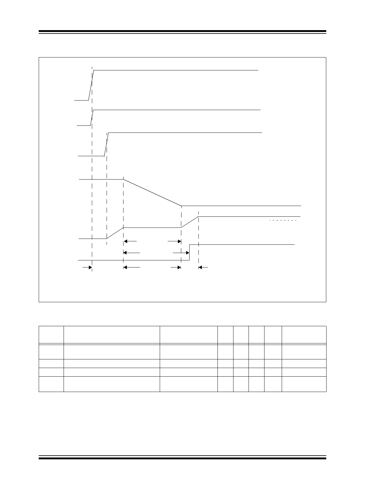
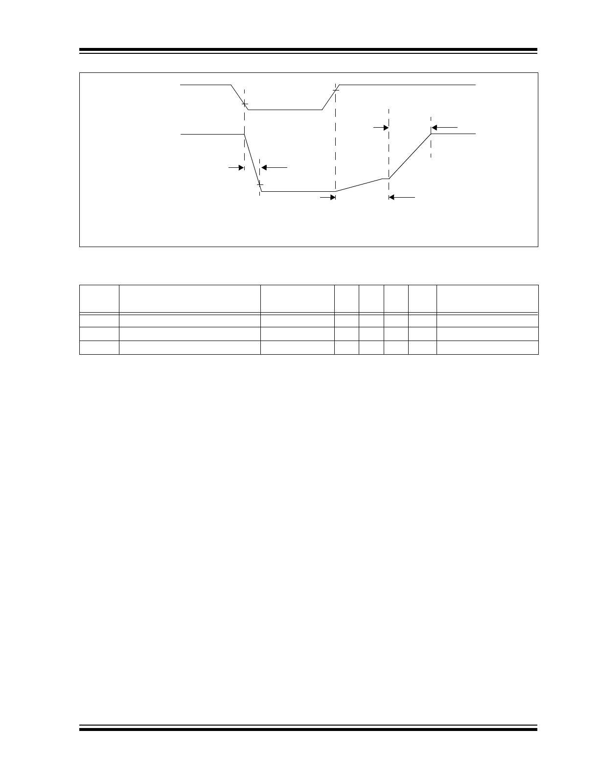
FIGURE 1-2:
Startup Waveforms.
TABLE 1-3:
STARTUP TIMING REQUIREMENTS
Param.
No.
Parameter
Sym
Min
Typ
Max Units
Conditions
MA000
UV
TH
/OV
TH
High (V
POS
applied) to
DRAIN
TH
falling
T
UVOV
H2
DTH
F
—
20.2
—
ms
MA001A DRAIN
TH
falling to PWRGOOD High
T
DTH
F2
GATE
PGH
—
19.3
—
ms
MA001B DRAIN
TH
falling to GATE Fast Ramp
T
DTH
F2
GATE
FR
—
13.1
—
ms
MA002
GATE Fast Ramp to external FET
fully enhanced
T
GATE
FR2FET
E
—
16.1
—
ms
Note:
Minimum and maximum specifications will be provided in future revisions of this data sheet.
PWRGOOD
UV
TH
OV
TH
V
REFOUT
< 2.5V
= 2.5V
> 2.5V
DRAIN
TH
MA000
MA001A
GATE
= 5V
(1)
= 12V
MA002
Note 1: This voltage is determined by the threshold voltage of the external FET.
This voltage needs to ensure the external FET is fully enhanced.
MA001B
2002-2012 Microchip Technology Inc.
DS20091C-page 9
MCP18480
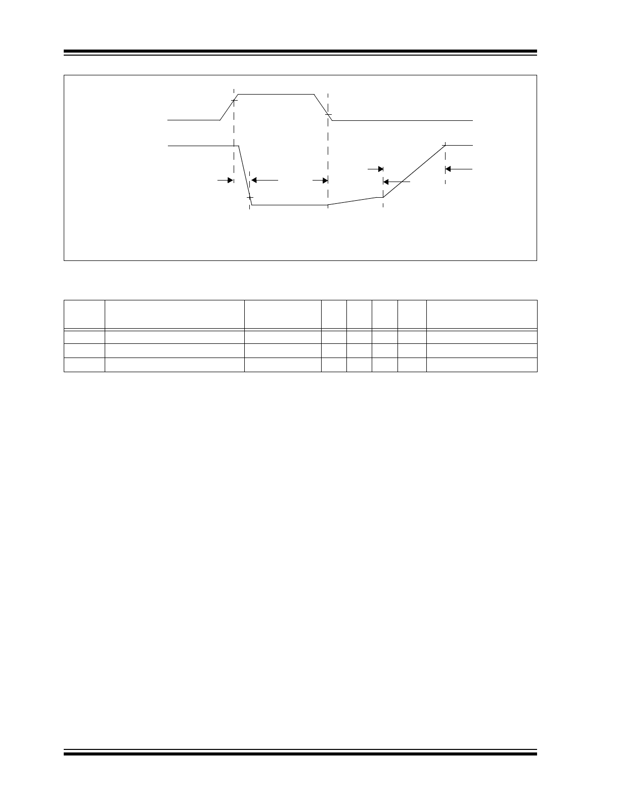
FIGURE 1-3:
ENABLE-to-GATE Waveforms.
TABLE 1-4:
ENABLE-TO-GATE TIMING REQUIREMENTS
Param.
No.
Parameter
Sym
Min
Typ
Max Units
Conditions
MA010
ENABLE Low to GATE Low
T
EN
L2
GATE
L
—
23.6
—
µs
MA011
ENABLE High to GATE Fast Ramp
T
EN
H2
GATE
FR
—
41
—
ms
MA012
GATE Fast Ramp to GATE High
T
GATE
FR2
GATE
H
—
17.8
—
ms
Note:
Minimum and maximum specifications will be provided in future revisions of this data sheet.
ENABLE
MA012
GATE
(1)
MA010
MA011
Note 1: This voltage is determined by the threshold voltage of the external FET.
This voltage needs to ensure the external FET is fully enhanced.
MCP18480
DS20091C-page 10
2002-2012 Microchip Technology Inc.
FIGURE 1-4:
OV
TH
-to-gate Waveform.
TABLE 1-5:
OV
TH
-TO-GATE TIMING REQUIREMENTS
Param.
No.
Parameter
Sym
Min
Typ
Max Units
Conditions
MA020
OV
TH
High to GATE Low
T
OV
H2
GATE
L
—
58.4
—
µs
MA021
OV
TH
Low to GATE Fast Ramp
T
OV
L2
GATE
FR
—
40.8
—
µs
MA022
GATE Fast Ramp to GATE High
T
GATE
FR2
GATE
H
—
17.8
—
ms
Note:
Minimum and maximum specifications will be provided in future revisions of this data sheet.
OV
TH
MA022
GATE
(1)
MA020
MA021
V
REFIN
+ V
OVO
- 20 mV
V
REFIN
+ V
OVO
Note 1: This voltage is determined by the threshold voltage of the external FET.
This voltage needs to ensure the external FET is fully enhanced.