

2014 Microchip Technology Inc.
DS20005311A-page 1
HV9921/HV9922/HV9923
Features
• Constant output current:
- HV9921 – 20mA
- HV9922 – 50mA
- HV9923 – 30mA
• Universal 85 - 264VAC operation
• Fixed off-time buck converter
• Internal 475V power MOSFET
Applications
• Decorative lighting
• Low power lighting fixtures
Description
HV9921/HV9922/HV9923 are pulse-width modulated
(PWM), high-efficiency, LED driver control ICs. They
allow efficient operation of LED strings from voltage
sources ranging up to 400VDC. HV9921/22/23 include
an internal high voltage switching MOSFET controlled
with fixed off-time (T
OFF
) of approximately 10μs. The
LED string is driven at constant current, thus providing
constant light output and enhanced reliability. The out-
put current is internally fixed at 20mA for HV9921,
50mA for HV992, and 30mA for HV9923. The peak cur-
rent control scheme provides good regulation of the
output current throughout the universal AC line voltage
range of 85 to 264VAC or DC input voltage of 20 to
400V.
3-Pin Switch-Mode LED Lamp Driver ICs

HV9921/HV9922/HV9923
DS20005311A-page 2
2014 Microchip Technology Inc.
TO OUR VALUED CUSTOMERS
It is our intention to provide our valued customers with the best documentation possible to ensure successful use of your Microchip
products. To this end, we will continue to improve our publications to better suit your needs. Our publications will be refined and
enhanced as new volumes and updates are introduced.
If you have any questions or comments regarding this publication, please contact the Marketing Communications Department via
E-mail at
docerrors@microchip.com
. We welcome your feedback.
Most Current Data Sheet
To obtain the most up-to-date version of this data sheet, please register at our Worldwide Web site at:
http://www.microchip.com
You can determine the version of a data sheet by examining its literature number found on the bottom outside corner of any page.
The last character of the literature number is the version number, (e.g., DS30000000A is version A of document DS30000000).
Errata
An errata sheet, describing minor operational differences from the data sheet and recommended workarounds, may exist for current
devices. As device/documentation issues become known to us, we will publish an errata sheet. The errata will specify the revision
of silicon and revision of document to which it applies.
To determine if an errata sheet exists for a particular device, please check with one of the following:
• Microchip’s Worldwide Web site;
http://www.microchip.com
• Your local Microchip sales office (see last page)
When contacting a sales office, please specify which device, revision of silicon and data sheet (include literature number) you are
using.
Customer Notification System
Register on our web site at
www.microchip.com
to receive the most current information on all of our products.
2014 Microchip Technology Inc.
DS20005311A-page 3
HV9921/HV9922/HV9923
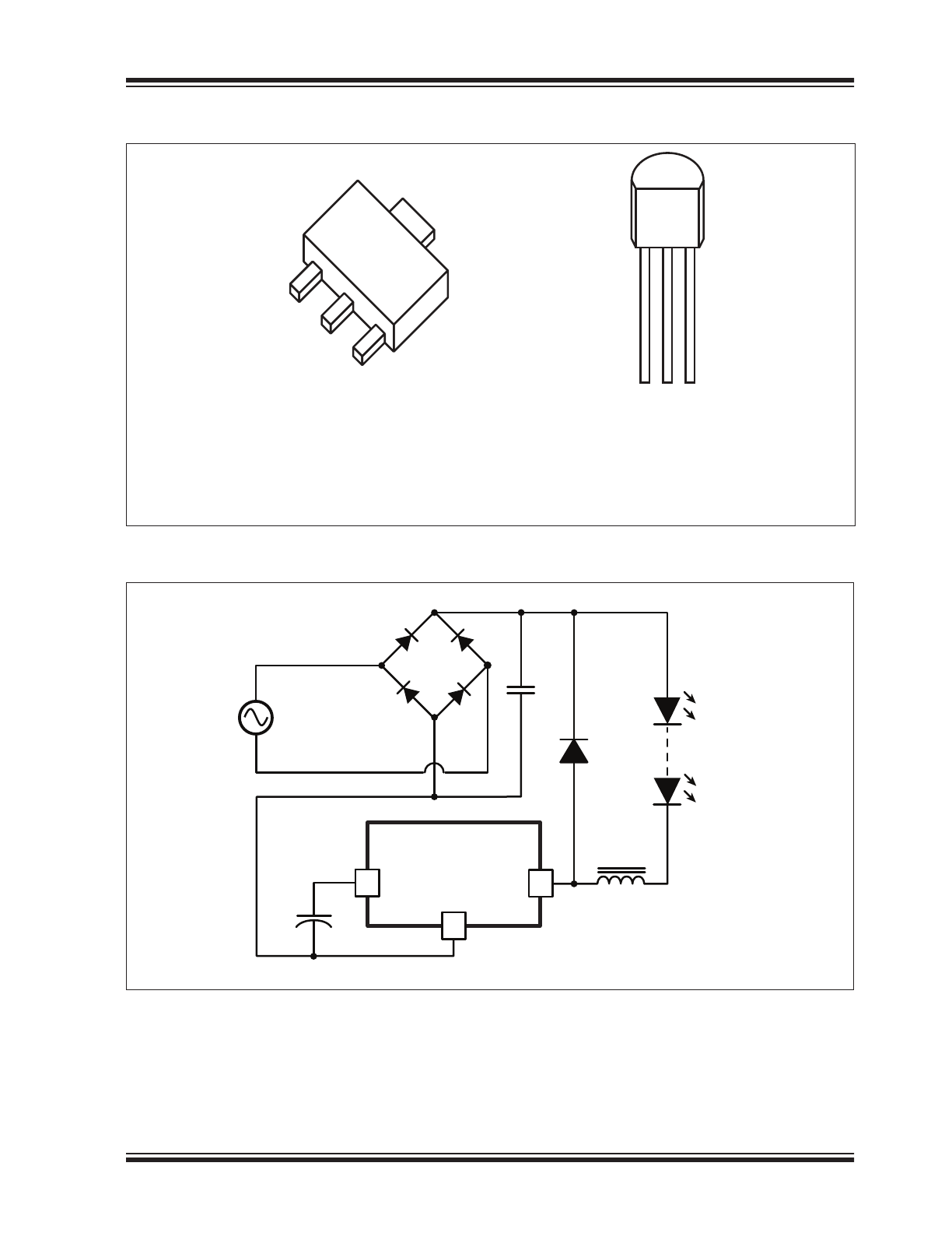
PIN DIAGRAM
TYPICAL APPLICATION CIRCUIT
1
2
3
1 2 3
TO-92
TO-243AA
(SOT-89)
See
Table 2-1
for Pin information.
HV9921/22/23
LED
1
-
LED
n
3 VDD
DRAIN 1
GND
2
AC
HV9921/HV9922/HV9923
DS20005311A-page 4
2014 Microchip Technology Inc.
1.0
ELECTRICAL CHARACTERISTICS
ABSOLUTE MAXIMUM RATINGS
Supply Voltage V
DD
................................ -0.3V to +10V
Supply Current I
DD
..............................................+5mA
Operating Ambient temperature ...........-40°C to +85°C
Operating Junction Temperature ........-40°C to +125°C
Storage temperature ..........................-65°C to +150°C
Power dissipation @+25°C for TO-92 .............740 mW
Power dissipation @+25°C for SOT-89....... 1600 mW*
* Mounted on FR4 board, 24mmx25mmx1.57mm
Note: Stresses above those listed under “Absolute
Maximum Ratings” may cause permanent damage to
the device. This is a stress rating only and functional
operation of the device at those or any other condi-
tions, above those indicated in the operational listings
of this specification, is not implied. Exposure to maxi-
mum rating conditions for extended periods may affect
device reliability.
1.1
ELECTRICAL SPECIFICATIONS
TABLE 1-1:
ELECTRICAL CHARACTERISTICS
1
Symbol
Parameter
Notes
Min
Typ
Max
Units Conditions
Regulator (V
DD
)
V
DD
V
DD
Regulator Output
-
-
7.5
-
V
V
DRAIN
V
DRAIN
Supply Voltage
-
20
-
-
V
V
UVLO
V
DD
Under-voltage Threshold
-
5.0
-
-
V
ΔV
UVLO
V
DD
Under-voltage Lockout Hysteresis
-
-
200
-
mV
I
DD
Operating Supply Current
-
-
200
350
μA
V
DD(EXT)
= 8.5V, V
DRAIN
= 40V
Output (DRAIN)
V
BR
Breakdown Voltage
2
475
-
-
V
R
ON
ON Resistance
-
-
-
210
Ω
I
DRAIN
= 20mA (HV9921)
I
DRAIN
= 50mA (HV9922)
I
DRAIN
= 30mA (HV9923)
C
DRAIN
Output Capacitance
3
-
1
5
pF
V
DRAIN
= 400V
I
SAT
MOSFET Saturation Current
3
100
150
-
mA
Current Sense Comparator
I
THL
Threshold Current - HV9921
2
18.5
-
25.5
mA
Threshold Current - HV9922
2
49
-
63
mA
Threshold Current - HV9923
2
28.2
-
38.2
mA
T
BLANK
Leading Edge Blanking Delay
2
,
3
200
300
400
ns
T
ON(MIN)
Minimum ON Time
-
-
-
650
ns
OFF-Time Generator
T
OFF
OFF Time
-
8
10.5
13
μS
1
Specifications are T
A
= 25°C, V
DRAIN
= 50V unless otherwise noted.
2
Applies over the full operating ambient temperature range of -40°C < T
A
< +125°C.
3
For design guidance only
2014 Microchip Technology Inc.
DS20005311A-page 5
HV9921/HV9922/HV9923
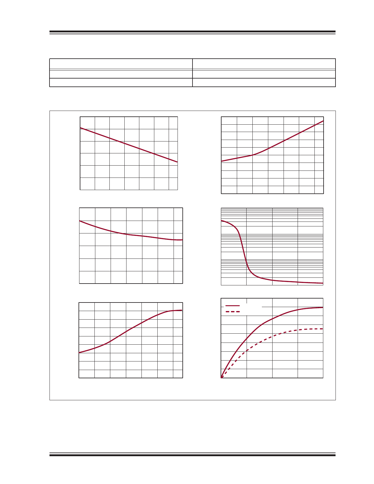
FIGURE 1-1:
TYPICAL PERFORMANCE CHARACTERISTICS (T
J
= 25°C UNLESS OTHERWISE NOTED)
THERMAL RESISTANCE
Package
θja
TO-92
132°C/W
TO-243AA(SOT-89)
133°C/W
200
180
160
140
120
100
80
60
40
20
0
Junction Temperature (°C)
ON Resistance (μΩ)
580
570
560
550
540
530
520
510
500
490
Junction Temperature (°C)
DRAIN Breakdown V
oltage (V)
180
160
140
120
100
80
60
40
20
0
DRAIN Voltage (V)
DRAIN Current (mA)
12
10
8
6
4
2
0
Junction Temperature (°C)
OFF T
ime (μS)
1000
100
10
1
0 10 20 30 40
DRAIN Voltage (V)
DRAIN Capacitance (pF)
T
J
= 25°C
T
J
= 125°C
1.10
1.05
1.00
0.95
0.90
0.85
0.80
-40 -15 10 35 60 85 110
Junction Temperature, °C
Normalized Threshold Current
-40 -15 10 35 60 85 110
-40 -15 10 35 60 85 110
-40 -15 10 35 60 85 110
0 10 20 30 40
HV9921/HV9922/HV9923
DS20005311A-page 6
2014 Microchip Technology Inc.
2.0
PIN DESCRIPTION
See
Pin Diagram on page 3
for the figures.
3.0
FUNCTIONAL DESCRIPTION
The HV9921/22/23 are PWM peak current controllers
designed to control a buck converter topology in contin-
uous conduction mode (CCM). The output current is
internally preset at 20mA for HV9921, 50mA for
HV992, and 30mA for HV9923.
When the input voltage of 20 to 400V appears at the
DRAIN pin, the internal high-voltage linear regulator
seeks to maintain a voltage of 7.5VDC at the V
DD
pin.
Until this voltage exceeds the internally programmed
under-voltage threshold, the output switching MOSFET
is non-conductive. When the threshold is exceeded,
the MOSFET turns on. The input current begins to flow
into the DRAIN pin. Hysteresis is provided in the under-
voltage comparator to prevent oscillation.
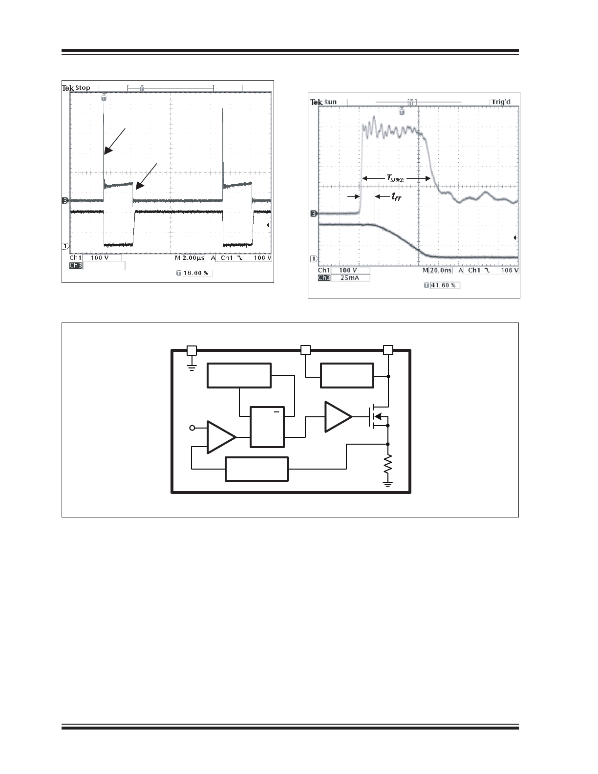
When the input current exceeds the internal preset
level, a current sense comparator resets an RS flip-
flop, and the MOSFET turns off. At the same time, a
one-shot circuit is activated that determines the dura-
tion of the off-state (10.5μs typical). As soon as this
time is over, the flip-flop sets again. The new switching
cycle begins.
A “blanking” delay of 300ns is provided that prevents
false triggering of the current sense comparator due to
the leading edge spike caused by circuit parasitics.
4.0
APPLICATION INFORMATION
HV9921/22/23 are low-cost off-line buck converter ICs
specifically designed for driving multi-LED strings.
They can be operated from either universal AC line
range of 85 to 264VAC, or 20 to 400VDC, and drive up
to tens of high-brightness LEDs. All LEDs can be run in
series, and the HV9921/22/23 regulate at constant cur-
rent, yielding uniform illumination. HV9921/22/23 are
compatible with triac dimmers. The output current is
internally fixed at 20mA for HV9921, 50mA for HV9922,
and 30mA for HV9923. These parts are available in
space saving TO-92 and SOT-89 packages.
4.1
Selecting L1 and D1
There is a certain trade-off to be considered between
optimal sizing of the output inductor L1 and the toler-
ated output current ripple. The required value of L1 is
inversely proportional to the ripple current ∆I
O
in it.
V
O
is the forward voltage of the LED string. T
OFF
is the
off-time of HV9921/22/23. The output current in the
LED string (I
O
) is calculated then as:
where I
TH
is the current sense comparator threshold.
The ripple current introduces a peak-to-average error
in the output current setting that needs to be accounted
for. Due to the constant off-time control technique used
in HV9921/22/23, the ripple current is independent of
the input AC or DC line voltage variation. Therefore, the
output current will remain unaffected by the varying
input voltage.
Adding a filter capacitor across the LED string can
reduce the output current ripple even further, thus per-
mitting a reduced value of L1. However, keep in mind
that the peak-to-average current error is affected by the
variation of T
OFF
. Therefore, the initial output current
accuracy might be sacrificed at large ripple current in
L1.
Another important aspect of designing an LED driver
with the HV9921/22/23 is related to certain parasitic
elements of the circuit, including distributed coil capac-
itance of L1, junction capacitance and reverse recovery
of the rectifier diode D1, capacitance of the printed cir-
cuit board traces C
PCB
and output capacitance C
DRAIN
of the controller itself. These parasitic elements affect
the efficiency of the switching converter and could
potentially cause false triggering of the current sense
comparator if not properly managed. Minimizing these
parasitics is essential for efficient and reliable operation
of the HV9921/22/23.
TABLE 2-1:
PIN DESCRIPTION
Pin #
Name
Description
1
Drain
Drain terminal of the output switching MOSFET and a linear regulator input
2
GND
Common connection for all circuits
3
VDD
Power Supply pin for all control circuits. By pass this pin with a 0.1 μF low-impedance
capacitor
L1
VO TOFF
IO
-------------------------------
=
IO ITH
1
2
---
IO
–
=

2014 Microchip Technology Inc.
DS20005311A-page 7
HV9921/HV9922/HV9923
Coil capacitance of inductors is typically provided in the
manufacturer’s data books either directly or in terms of
the self-resonant frequency (SRF).
where L is the inductance value, and C
L
is the coil
capacitance.) Charging and discharging this capaci-
tance every switching cycle causes high-current spikes
in the LED string. Therefore, connecting a small capac-
itor C
O
(~10nF) is recommended to bypass these
spikes.
Using an ultra-fast rectifier diode for D1 is recom-
mended to achieve high efficiency and reduce the risk
of false triggering of the current sense comparator.
Using diodes with shorter reverse recovery time, t
rr
,
and lower junction capacitance, C
J
, achieves better
performance. The reverse voltage rating, V
R
, of the
diode must be greater than the maximum input voltage
of the LED lamp.
The total parasitic capacitance present at the DRAIN
pin of the HV9921/22/23 can be calculated as:
When the switching MOSFET turns on, the capaci-
tance C
P
is discharged into the DRAIN pin of the IC.
The discharge current is limited to about 150mA typi-
cally. However, it may become lower at increased junc-
tion temperature. The duration of the leading edge
current spike can be estimated as:
In order to avoid false triggering of the current sense
comparator, C
P
must be minimized in accordance with
the following expression:
where T
BLANK(MIN)
is the minimum blanking time of
200ns, and V
IN(MAX)
is the maximum instantaneous
input voltage.
4.2
Estimating Power Loss
Discharging the parasitic capacitance CP into the
DRAIN pin of the HV9921/22/23 is responsible for the
bulk of the switching power loss. It can be estimated
using the following equation:
where F
S
is the switching frequency, I
SAT
is the satu-
rated DRAIN current of the HV9921/22/23. The switch-
ing loss is the greatest at the maximum input voltage.
The switching frequency is given by the following equa-
tion.
When the HV9921/22/23 LED driver is powered from
the full-wave rectified AC input, the switching power
loss can be estimated as:
V
AC
is the input AC line voltage.
The switching power loss associated with turn-off tran-
sitions of the DRAIN pin can be disregarded. Due to the
large amount of parasitic capacitance connected to this
switching node, the turn-off transition occurs essen-
tially at zero-voltage.
Conduction power loss in the HV9921/22/23 can be
calculated as:
where D = V
O
/V
IN
is the duty ratio, R
ON
is the on-resis-
tance, I
DD
is the internal linear regulator current.
When the LED driver is powered from the full-wave rec-
tified AC line input, the exact equation for calculating
the conduction loss is more cumbersome. However, it
can be estimated using the following equation:
where V
AC
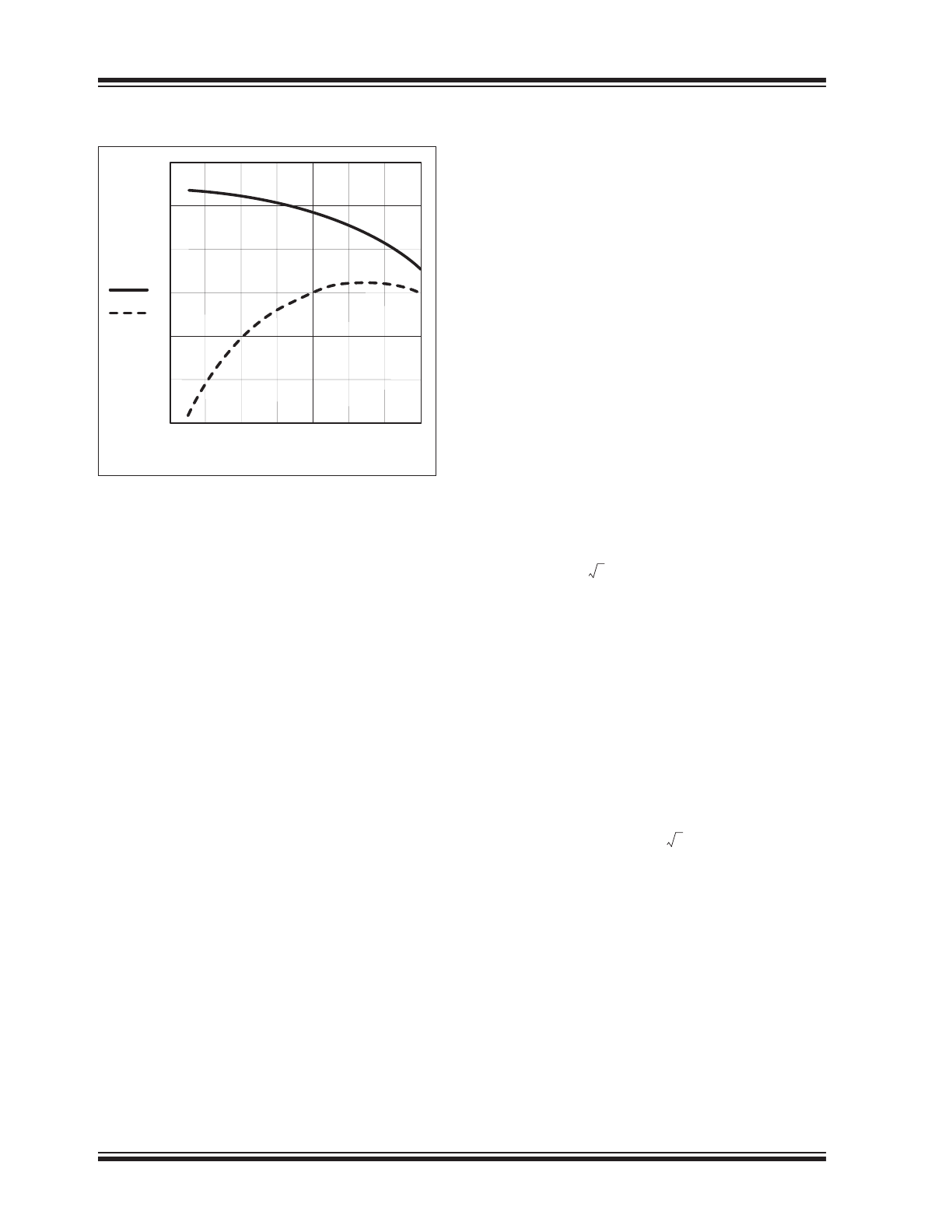
is the input AC line voltage. The coefficients
K
C
and K
d
can be determined from the minimum duty
ratio of the HV9921/22/23.
SRF
1
2
L CL
=
C
P
C
DRAIN
C
PCB
C
L
C
J
+
+
+
=
T
SPIKE
V
IN
C
P
I
SAT
-------------------- t
rr
+
=
C
P
I
SAT
T
BLANK MIN
t
rr
–
V
IN MAX
---------------------------------------------------------
P
SWITCH
V
IN
2
C
P
2
------------------ V
IN
I
SAT
t
rr
+
F
S
=
F
S
V
IN
V
O
–
V
IN
T
OFF
-------------------------
=
P
SWITCH
1
2 T
OFF
-------------------- V
AC
C
P
2 I
SAT
t
rr
+
V
AC
V
O
–
P
COND
D I
O
2
R
ON
I
DD
V
IN
1 D
–
+
=
P
COND
K
C
I
O
2
R
ON
K
d
I
DD
V
AC
+
=
HV9921/HV9922/HV9923
DS20005311A-page 8
2014 Microchip Technology Inc.
FIGURE 4-1:
CONDUCTION LOSS
COEFFICIENTS K
C
AND K
d
4.3
EMI Filter
As with all off-line converters, selecting an input filter is
critical to obtaining good EMI. A switching side capaci-
tor, albeit of small value, is necessary in order to ensure
low impedance to the high frequency switching cur-
rents of the converter. As a rule of thumb, this capacitor
should be approximately 0.1-0.2 μF/W of LED output
power. A recommended input filter is shown in
Figure 4-2
for the following design example.
4.3.1
DESIGN EXAMPLE
The following example designs a HV9921 LED lamp
driver meeting the following specifications:
• Input: Universal AC, 85-265VAC
• Output Current: 20mA
• Load: String of 10 LED (LW541C by OSRAM VF
= 4.1V max. each)
4.3.1.1
Step 1. Calculating L1.
The output voltage V
O
= 10 x V
F
≈ 41V (max.). Use this
equation assuming a 30% peak-to-peak ripple.
Select L1 68mH, I = 30mA. Typical SRF = 170KHz.
Calculate the coil capacitance.
4.3.1.2
Step 2. Selecting D1
Usually, the reverse recovery characteristics of ultra-
fast rectifiers at I
F
= 20 ~ 50mA are not provided in the
manufacturer’s data books. The designer may want to
experiment with different diodes to achieve the best
result.
Select D1 MUR160 with V
R
= 600V, t
rr
≈ 20ns (I
F
=
20mA, I
RR
= 100mA) and C
J
≈ 8pF (VF > 50V).
4.3.1.3
Step 3. Calculating total parasitic
capacitance
4.3.1.4
Step 4. Calculating the leading edge
spike duration
4.3.1.5
Step 5. Estimating power dissipation
in HV9921 at 265VAC
Switching power loss:
Minimum duty ratio:
Conduction power loss:
Total power dissipation in HV9921:
0 0.1 0.2 0.3 0.4 0.5 0.6 0.7
0.7
0.6
0.5
0.4
0.3
0.2
0.1
Kd(Dm)
Kc(Dm)
Dm
L1 41V 10.5s
0.3 20mA
---------------------------------- 72mH
=
=
C
L
1
L1
2
SRF
2
------------------------------------------
1
68mH
2
170KHz
2
------------------------------------------------------------- 13pF
=
=
=
C
p
5pF 5pF 13pF 8pF 13pF
=
+
+
+
=
T
SPIKE
264V
2 31pF
100mA
-------------------------------------------- 20ns 136ns T
BLANK MIN
+
=
P
SWITCH
1
2 10.5
s
-------------------------- 264V 31pF 2 100mA 20ns
+
264V 41V
–
131mW
D
M
41V
265V
2
-------------------------- 0.11
=
P
COND
0.25
20mA
2
210
0.63 200
A 264V
55mW
+
=
P
TOTAL
131mW 55mW 186mW
=
+
=
2014 Microchip Technology Inc.
DS20005311A-page 9
HV9921/HV9922/HV9923
4.3.1.6
Step 6. Selecting input capacitor C
IN
Select C
IN
ECQ-E4104KF by Panasonic
®
(0.1μF,
400V, Metalized Polyester Film).
FIGURE 4-2:
UNIVERSAL 85-264VAC LED LAMP DRIVER
FIGURE 4-3:
TYPICAL EFFICIENCY
FIGURE 4-4:
SWITCH-OFF TRANSITION
Ch1:V
DRAIN
, Ch3: I
DRAIN
OutputPower 41V 20mA 820mW
=
=
C
IN
AC Line
85-265V
C
DD
3
HV9921/22/23
D1
L1
LED
1
- LED
12
D2
D3
D4 D5
C
IN2
L
IN
VRD1
F1
C
O
VDD
DRAIN
GND
1
2
75 100 125 150 175 200 225 250 275
82
80
78
76
74
72
70
68
66
64
62
Input AC Line Voltage (VAC)
Efficiency (%)
ZERO VOLTAGE
TRANSITION
HV9921/HV9922/HV9923
DS20005311A-page 10
2014 Microchip Technology Inc.
FIGURE 4-5:
TYPICAL EFFICIENCY
FIGURE 4-6:
SWITCH-OFF TRANSITION
Ch1:V
DRAIN
, Ch3: I
DRAIN
FIGURE 4-7:
FUNCTIONAL BLOCK DIAGRAM
LEADING EDGE SPIKE
25mA
SWITCH OFF
VDD
REF
R
DRAIN
GND
HV9921/HV9922/HV9923
Regulator
7.5V
T
BLANK
= 300ns
+
-
S
R
Q
Q
T
OFF
= 10.5μs