
2013 Microchip Technology Inc.
DS20005208A-page 1
MCP1643
Features
• 1.6A Typical Peak Input Current Limit
• Up to 550 mA LED Load Current
• Low Start-up Voltage: 0.65V (typical, 25 mA LED
Current)
• Low Operating Input Voltage: down to 0.5V
• Maximum Input Voltage < V
LED
< 5.0V
• Maximum Output Voltage:
- 5.0V
- Overvoltage Protection
• Low Reference Voltage:
- V
FB
= 120 mV
- Minimal Power Loss on Sense Resistor
• Pulse-Width Modulation Mode Operation (1 MHz)
• Internal Synchronous Rectifier
• Internal Compensation
• Inrush Current Limiting
• Internal Soft-Start (240 µs typical)
• Shutdown (EN = GND):
- True Load Disconnect
- Dimming Control by Variable Duty Cycle
• Shutdown Current: 1.2 µA (typical)
• Overtemperature protection
• Packages:
- MSOP-8
- 2x3 DFN-8
Applications
• One and Two Cell Alkaline and NiMH/NiCd
Portable LED Lighting Products
• LED Flashlight and Head Lamps
• Rechargeable Flashlights
• Wall LED Lamps with Motion Detectors
• LED supply for backlights
• General LED constant current applications
Description
MCP1643 is a compact, high-efficiency, fixed
frequency, synchronous step-up converter optimized to
drive one LED with constant current, that operates from
one and two-cell alkaline and NiMH/NiCd batteries.
The device can also drive two red/green/yellow series
connection LEDs.
Low-voltage technology allows the regulator to start up
without high-output voltage and load-current overshoot
from a low 0.65V input. High efficiency is accomplished
by integrating the low resistance N-Channel Boost
switch and synchronous P-Channel switch. All
compensation and protection circuitry are integrated to
minimize external components.
The internal feedback (V
FB
) voltage is set to 120 mV for
low power dissipation when sensing and regulating
LED current. A single resistor sets the constant current
output that drives the LED load.
The device features an output overvoltage protection
that limits the output voltage to 5.0V typical, in case the
LED fails or output load is disconnected.
The LED will either be turned OFF or turned ON using
the enable input. A True Output Load Disconnect mode
provides input-to-output isolation while Shutdown
(EN = GND) by removing the normal boost regulator
diode path from input to output. Shutdown state
consumes 1.2 µA from input at room temperature.
The LED can be turned on and off with a variable duty
cycle pulse-width modulation (PWM) signal applied to
the EN pin for dimming applications.
The device also features a thermal shutdown at
+150°C, with +25°C hysteresis.
Two package options, MSOP-8 and 2x3 DFN-8, are
available.
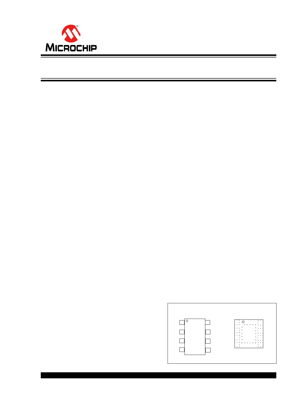
Package Types
MCP1643
2x3 DFN*
NC
V
FB
V
OUT
S
GND
P
GND
1
2
3
4
8
7
6
5 SW
V
IN
EN
EP
9
6
1
2
3
8 V
IN
P
GND
EN
V
FB
NC
7 S
GND
MCP1643
MSOP-8
5
4
SW
V
OUT
* Includes Exposed Thermal Pad (EP), see
Table 3-1
.
1 MHz Low Start-up Voltage Synchronous Boost
LED Constant Current Regulator
MCP1643
DS20005208A-page 2
2013 Microchip Technology Inc.
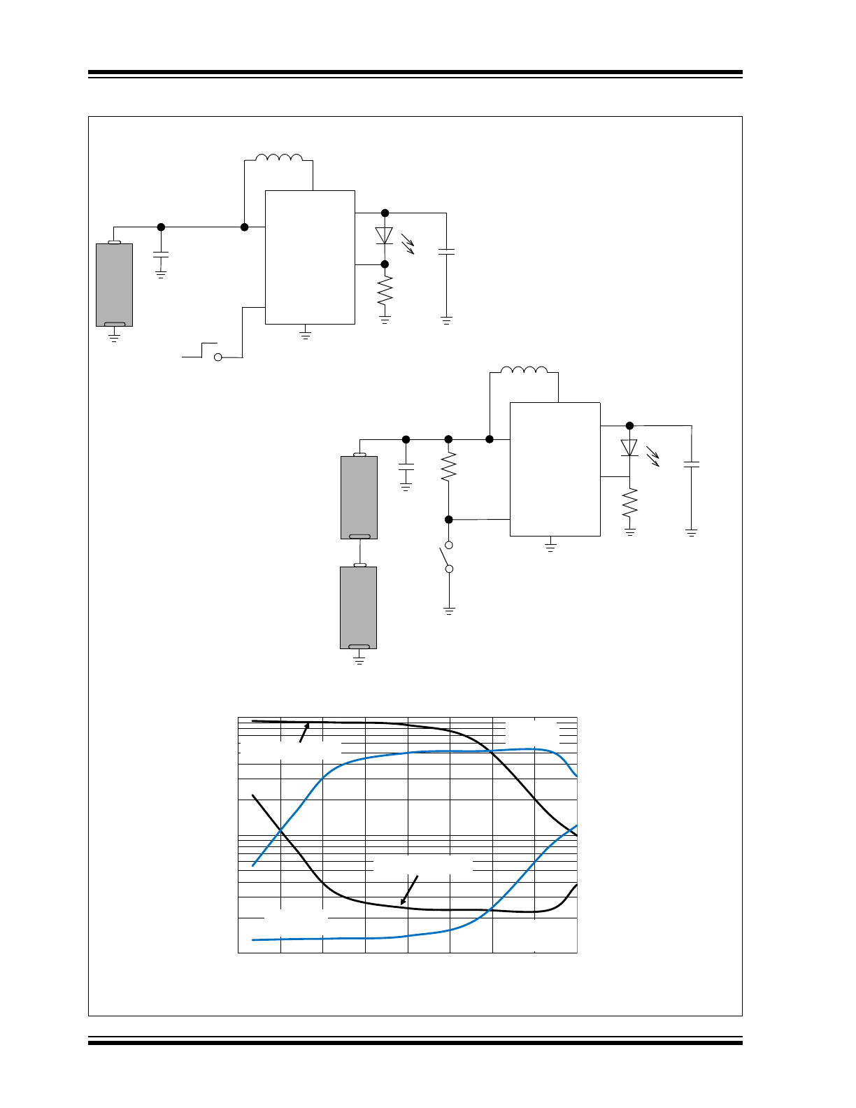
Typical Applications
10
100
1000
0.1
1
10
0.6 0.9 1.2 1.5 1.8 2.1 2.4 2.7 3
LED Current (mA
)
R
SET
(
Ω
)
Input Voltage (V)
R
SET
for I
LED
MIN
I
LED MIN
I
LED MAX
R
SET
for I
LED
MAX
T
A
= +25
o
C
V
IN
GND
V
FB
C
OUT
4.7 µF
C
IN
4.7...10 µF
L
1
4.7 µH
SW
LED
4.7
EN
V
OUT
+
-
A
L
KA
L
INE
ON
OFF
MCP1643
I
LED
= 25 mA
R
SET
V
IN
GND
V
FB
C
OUT
20 µF
C
IN
4.7...10 µF
L
1
4.7 µH
SW
WHITE LED
0.33
EN
V
OUT
+
-
NI
M
H
1.
2V
ON/OFF
MCP1643
I
LED
= 360 mA
R
SET
+
-
NI
M
H
1.
2V
1 M
R
EN
I
L ED
0.12 V
R
SET
-----------------
=
R
SET
Minimum and Maximum Limits for I
LED
in Regulation, with ±6% Tolerance
WHITE LED
I
LED MAX
I
LED MIN
2013 Microchip Technology Inc.
DS20005208A-page 3
MCP1643
1.0
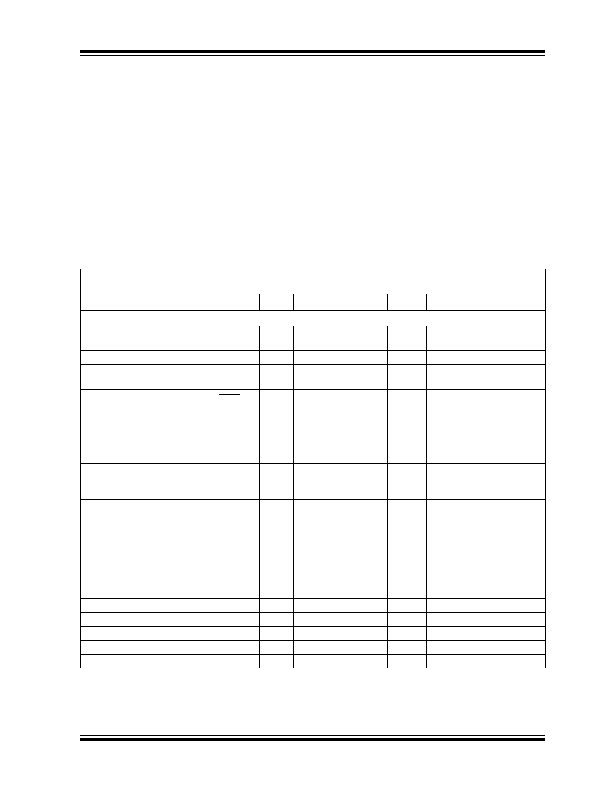
ELECTRICAL
CHARACTERISTICS
Absolute Maximum Ratings †
EN, FB, V
IN,
V
SW
, V
OUT
- GND ........................... +6.5V
EN, FB ......... < maximum V
OUT
or V
IN
> (GND – 0.3V)
Output Short Circuit Current....................... Continuous
Power Dissipation ............................ Internally Limited
Storage Temperature ......................... -65°C to +150°C
Ambient Temp. with Power Applied...... -40°C to +85°C
Operating Junction Temperature........ -40°C to +125°C
ESD Protection On All Pins:
HBM .............................................................. 4 kV
MM................................................................ 300V
† Notice: Stresses above those listed under “Maximum
Ratings” may cause permanent damage to the device.
This is a stress rating only and functional operation of
the device at those or any other conditions above those
indicated in the operational sections of this
specification is not intended. Exposure to maximum
rating conditions for extended periods may affect
device reliability.
DC CHARACTERISTICS
Electrical Characteristics: Unless otherwise indicated, V
IN
= EN = 1.2V, C
OUT
= 20 µF, C
IN
= 10 µF, L = 4.7 µH,
I
LED
= 25 mA, T
A
= +25°C. Boldface specifications apply over the T
A
range of -40°C to +85°C.
Parameters
Sym
Min
Typ
Max
Units
Conditions
Input Characteristics
Minimum Input Voltage
After Start-Up
V
IN
—
0.5
—
V
Note 1
,
Note 3
Start-Up Voltage
V
IN
—
0.65
0.8
V
Note 2
,
Note 1
Output Overvoltage
Protection
V
OUT_OVP
—
5.0
—
V
Note 3
Shutdown
Quiescent Current
I
QSHDN
—
1.2
—
µA
EN = GND;
includes N-Channel and
P-Channel Switch Leakage
Feedback Voltage
V
FB
105
120
135
mV
Feedback Input
Bias Current
I
VFB
—
60
—
pA
NMOS Switch Leakage
I
NLK
—
0.4
—
µA
V
IN
= V
SW
= 4.0V
V
OUT
= 4.5V
V
EN
= V
FB
= GND
PMOS Switch Leakage
I
PLK
—
0.25
—
µA
V
IN
= VS
W
= GND;
V
OUT
= 4.5V
NMOS Switch
ON Resistance
R
DS(ON)N
—
0.2
—
I
LED
= 250 mA,
Note 3
PMOS Switch
ON Resistance
R
DS(ON)P
—
0.4
—
I
LED
= 250 mA,
Note 3
NMOS Peak
Switch Current Limit
I
N(MAX)
—
1.6
—
A
Note 3
Maximum Duty Cycle
DC
MAX
—
90
—
%
Note 3
Minimum Duty Cycle
DC
MIN
—
5
—
%
Note 3
Switching Frequency
f
SW
0.85
1.0
1.15
MHz
EN Input Logic High
V
IH
75
—
—
%of V
IN
I
LED
= 25 mA
EN Input Logic Low
V
IL
—
—
20
%of V
IN
I
LED
= 25 mA
Note 1:
For V
IN
< V
OUT
, I
LED
remains in regulation up to V
IN
= V
LED
minus a headroom @ LED typical V
F
and I
F
.
2:
V
OUT
completely discharged. If the output capacitor remains partially charged, the device will start-up at
the minimum possible voltage.
3:
Determined by characterization, not production tested.
MCP1643
DS20005208A-page 4
2013 Microchip Technology Inc.
EN Input Leakage Current
I
ENLK
—
0.9
—
µA
V
EN
= 1.2V
Soft Start Time
t
SS
—
240
—
µs
EN Low-to-High,
90% of V
OUT
;
I
LED
= 25 mA,
Note 3
—
270
—
µs
EN Low-to-High,
90% of V
OUT
;
I
LED
= 300 mA,
Note 3
Thermal Shutdown
Die Temperature
T
SD
—
150
—
C
I
LED
= 25 mA
Die Temperature
Hysteresis
T
SDHYS
—
25
—
C
DC CHARACTERISTICS (CONTINUED)
Electrical Characteristics: Unless otherwise indicated, V
IN
= EN = 1.2V, C
OUT
= 20 µF, C
IN
= 10 µF, L = 4.7 µH,
I
LED
= 25 mA, T
A
= +25°C. Boldface specifications apply over the T
A
range of -40°C to +85°C.
Parameters
Sym
Min
Typ
Max
Units
Conditions
Note 1:
For V
IN
< V
OUT
, I
LED
remains in regulation up to V
IN
= V
LED
minus a headroom @ LED typical V
F
and I
F
.
2:
V
OUT
completely discharged. If the output capacitor remains partially charged, the device will start-up at
the minimum possible voltage.
3:
Determined by characterization, not production tested.
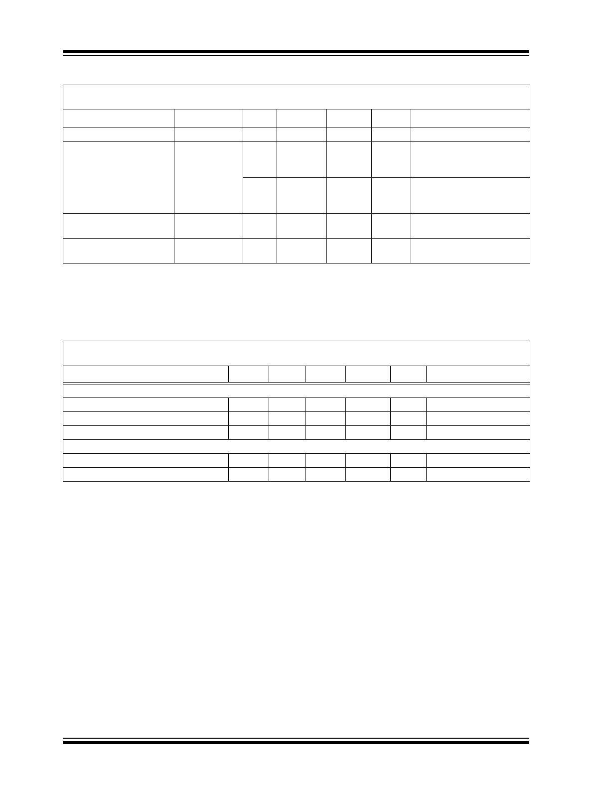
TEMPERATURE SPECIFICATIONS
Electrical Characteristics: Unless otherwise indicated, V
IN
= EN = 1.2V, C
OUT
= 20 µF, C
IN
= 10 µF, L = 4.7 µH,
I
LED
= 25 mA, T
A
= +25°C. Boldface specifications apply over the T
A
range of -40°C to +85°C.
Parameters
Sym
Min
Typ
Max
Units
Conditions
Temperature Ranges
Operating Ambient Temperature Range
T
A
-40
—
+85
°C
Steady State
Storage Temperature Range
T
A
-65
—
+150
°C
Maximum Junction Temperature
T
J
—
—
+150
°C
Transient
Package Thermal Resistances
Thermal Resistance, 8L-2x3 DFN
JA
—
68
—
°C/W
Thermal Resistance, 8L-MSOP
JA
—
211
—
°C/W
2013 Microchip Technology Inc.
DS20005208A-page 5
MCP1643
2.0
TYPICAL PERFORMANCE CURVES
Note: Unless otherwise indicated, V
IN
= EN = 1.2V, C
OUT
= 20 µF, C
IN
= 10 µF, L = 4.7 µH, I
LED
= 25 mA, T
A
= +25°C,
MSOP-8 package.
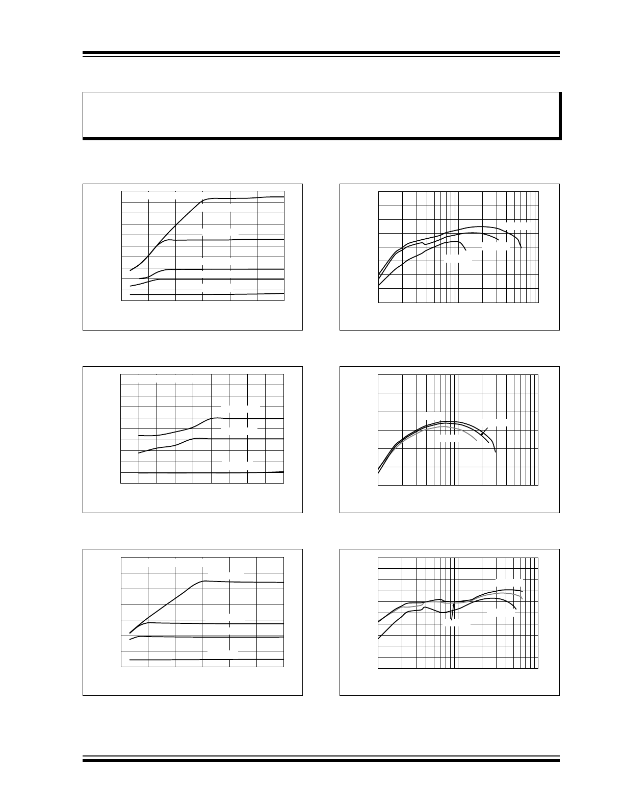
FIGURE 2-1:
One White LED I
LED
vs. V
IN
.
FIGURE 2-2:
One Red LED I
LED
vs. V
IN
.
FIGURE 2-3:
Two Series Connection Red
LEDs I
LED
vs. V
IN
.
FIGURE 2-4:
One White LED Efficiency
vs. I
LED
.
FIGURE 2-5:
One Red LED Efficiency vs.
I
LED
.
FIGURE 2-6:
Two Red LEDs Efficiency (in
Series Connection) vs. I
LED
.
Note:
The graphs and tables provided following this note are a statistical summary based on a limited number of
samples and are provided for informational purposes only. The performance characteristics listed herein
are not tested or guaranteed. In some graphs or tables, the data presented may be outside the specified
operating range (e.g., outside specified power supply range) and therefore outside the warranted range.
0
50
100
150
200
250
300
350
400
450
500
0.6
0.9
1.2
1.5
1.8
2.1
2.4
LED Current (mA)
Input Voltage (V)
R
SET
= 5
ȍ
R
SET
= 1.2
ȍ
R
SET
= 0.82
ȍ
R
SET
= 0.41
ȍ
R
SET
= 0.25
ȍ
LED V
F
= 3.5V @ I
F
= 700 mA
0
25
50
75
100
125
150
175
200
225
250
0.6
0.7
0.8
0.9
1
1.1
1.2
1.3
1.4
1.5
LED Current (mA)
Input Voltage (V)
R
SET
= 5
ȍ
LED V
F
= 2.5V @ I
F
= 350 mA
R
SET
= 1.2
ȍ
R
SET
= 0.82
ȍ
0
50
100
150
200
250
300
350
0.6
0.9
1.2
1.5
1.8
2.1
2.4
LEDs Current (mA)
Input Voltage (V)
R
SET
= 5
ȍ
R
SET
= 1.2
ȍ
R
SET
= 0.82
ȍ
R
SET
= 0.41
ȍ
LED V
F
= 2.5V @ I
F
= 350 mA
60
65
70
75
80
85
90
95
100
10
100
1000
Efficiency
(%
)
I
LED
(mA)
V
IN
= 1.2V
V
IN
= 1.8V
V
IN
= 2.4V
70
75
80
85
90
95
100
10
100
1000
Efficiency
(%
)
I
LED
(mA)
V
IN
= 1.2V
V
IN
= 1.8V
V
IN
= 2.4V
50
55
60
65
70
75
80
85
90
95
100
10
100
1000
Efficiency
(%
)
I
LED
(mA)
V
IN
= 3.0V
V
IN
= 2.4V
V
IN
= 3.6V
MCP1643
DS20005208A-page 6
2013 Microchip Technology Inc.
Note: Unless otherwise indicated, V
IN
= EN = 1.2V, C
OUT
= 20 µF, C
IN
= 10 µF, L = 4.7 µH, I
LED
= 25 mA, T
A
= +25°C,
MSOP-8 package.
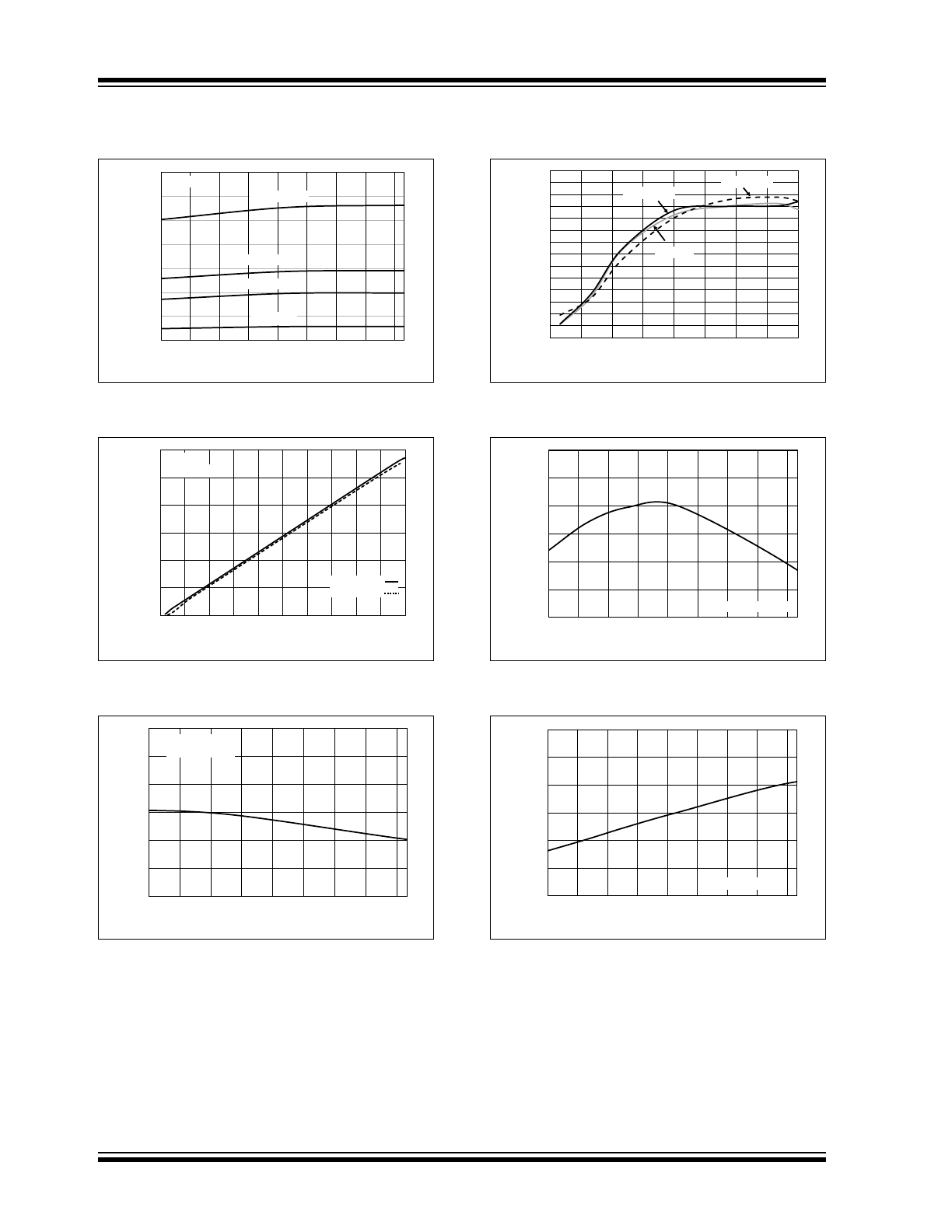
FIGURE 2-7:
One White I
LED
vs. Ambient
Temperature.
FIGURE 2-8:
I
LED
vs. V
EN
Duty Cycle.
FIGURE 2-9:
Duty Cycle vs. Ambient
Temperature.
FIGURE 2-10:
Maximum I
LED
vs. V
IN
.
FIGURE 2-11:
f
SW
vs. Ambient
Temperature.
FIGURE 2-12:
V
FB
vs. Ambient
Temperature.
0
50
100
150
200
250
300
350
-40
-25
-10
5
20
35
50
65
80
LED Current (mA)
Ambient Temperature (°C)
R
SET
= 5
ȍ
R
SET
= 1.2
ȍ
R
SET
= 0.82
ȍ
R
SET
= 0.41
ȍ
V
IN
= 1.5V
0
25
50
75
100
125
150
0
10
20
30
40
50
60
70
80
90 100
LED Current (mA)
Duty Cycle (%)
R
SET
= 0.82
ȍ
V
IN
= 1.5V
f
EN
= 400 Hz
f
EN
= 1 kHz
34
35
36
37
38
39
40
-40
-25
-10
5
20
35
50
65
80
Duty
Cy
cle (%
)
Ambient Temperature (°C)
R
SET
= 1.2
ȍ
(I
LED
= 100 mA)
0
100
200
300
400
500
600
700
0.6
0.9
1.2
1.5
1.8
2.1
2.4
2.7
3
LED Current (mA)
Input Voltage (V)
T
A
= +85
o
C
T
A
= +25
o
C
T
A
= 0
o
C
980
985
990
995
1000
1005
1010
-40
-25
-10
5
20
35
50
65
80
Sw
itching Frequency
(kHz)
Ambient Temperature (°C)
I
LED
= 100 mA
117
118
119
120
121
122
123
-40
-25
-10
5
20
35
50
65
80
Feadback V
o
ltage (mV)
Ambient Temperature (°C)
I
LED
= 100 mA
2013 Microchip Technology Inc.
DS20005208A-page 7
MCP1643
Note: Unless otherwise indicated, V
IN
= EN = 1.2V, C
OUT
= 20 µF, C
IN
= 10 µF, L = 4.7 µH, I
LED
= 25 mA, T
A
= +25°C,
MSOP-8 package.
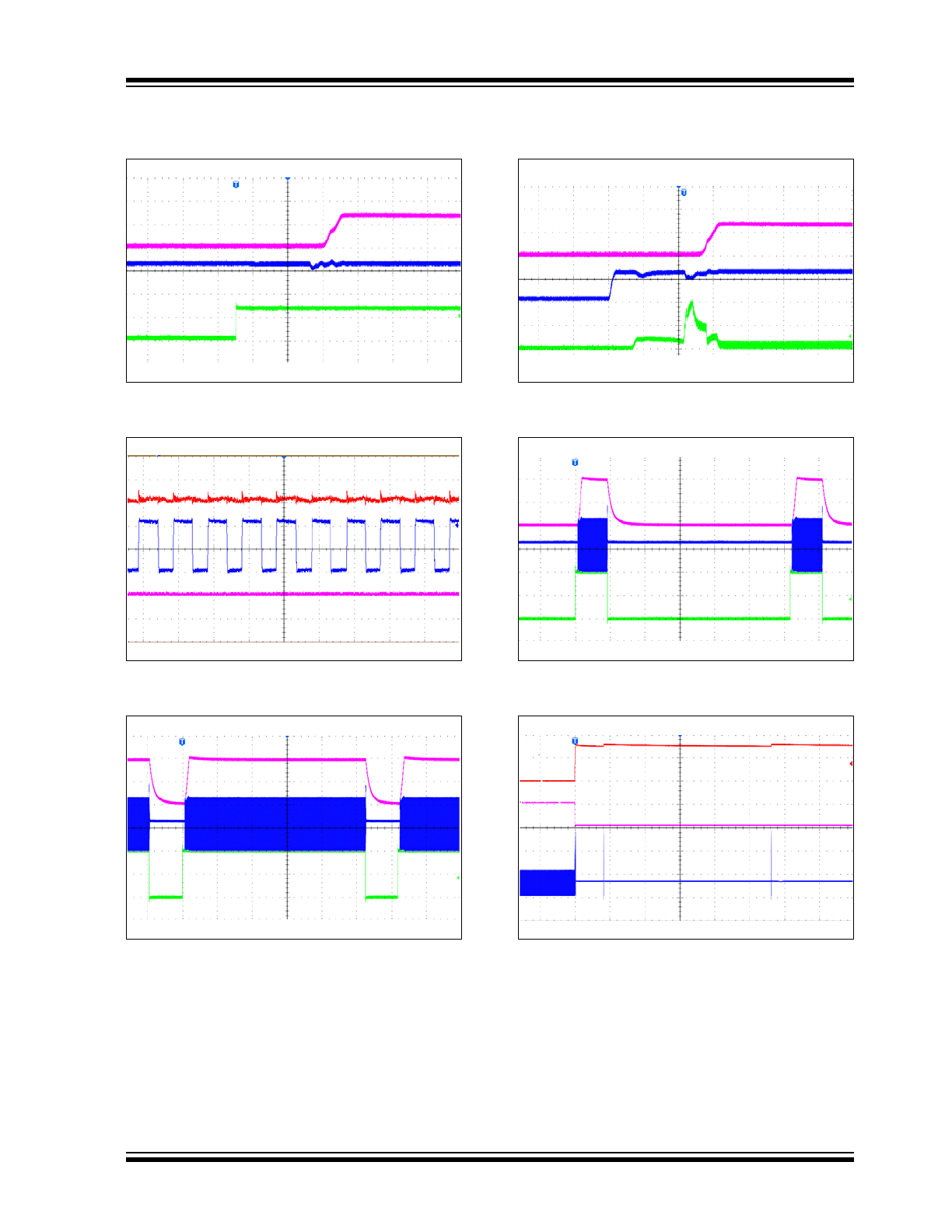
FIGURE 2-13:
Start-up After Enable.
FIGURE 2-14:
100 mA PWM Operation.
FIGURE 2-15:
400 Hz PWM Dimming,
85% Duty Cycle.
FIGURE 2-16:
Start-up when V
IN
= V
EN
.
FIGURE 2-17:
400 Hz PWM Dimming,
15% Duty Cycle.
FIGURE 2-18:
Open Load Response.
V
EN
80 us/div
1 V/div
V
IN
I
LED
20 mA/div
20 mV/div, AC Coupled
V
OUT
1 V/div
V
SW
I
LED
100 mA/div
1 us/div
I
LED
50 mA/div
1 V/div
V
SW
1 V/div
V
EN
400 us/div
80 us/div
500 mA/div
I
L
1 V/div
V
IN
I
LED
20 mA/div
I
LED
50 mA/div
1 V/div
V
SW
1 V/div
V
EN
400 us/div
I
LED
10 ms/div
2 V/div
Step from I
LED
= 100 mA to Open Load
2 V/div
100 mA/div
V
OUT
V
SW
2V
5V

MCP1643
DS20005208A-page 8
2013 Microchip Technology Inc.
NOTES:
2013 Microchip Technology Inc.
DS20005208A-page 9
MCP1643
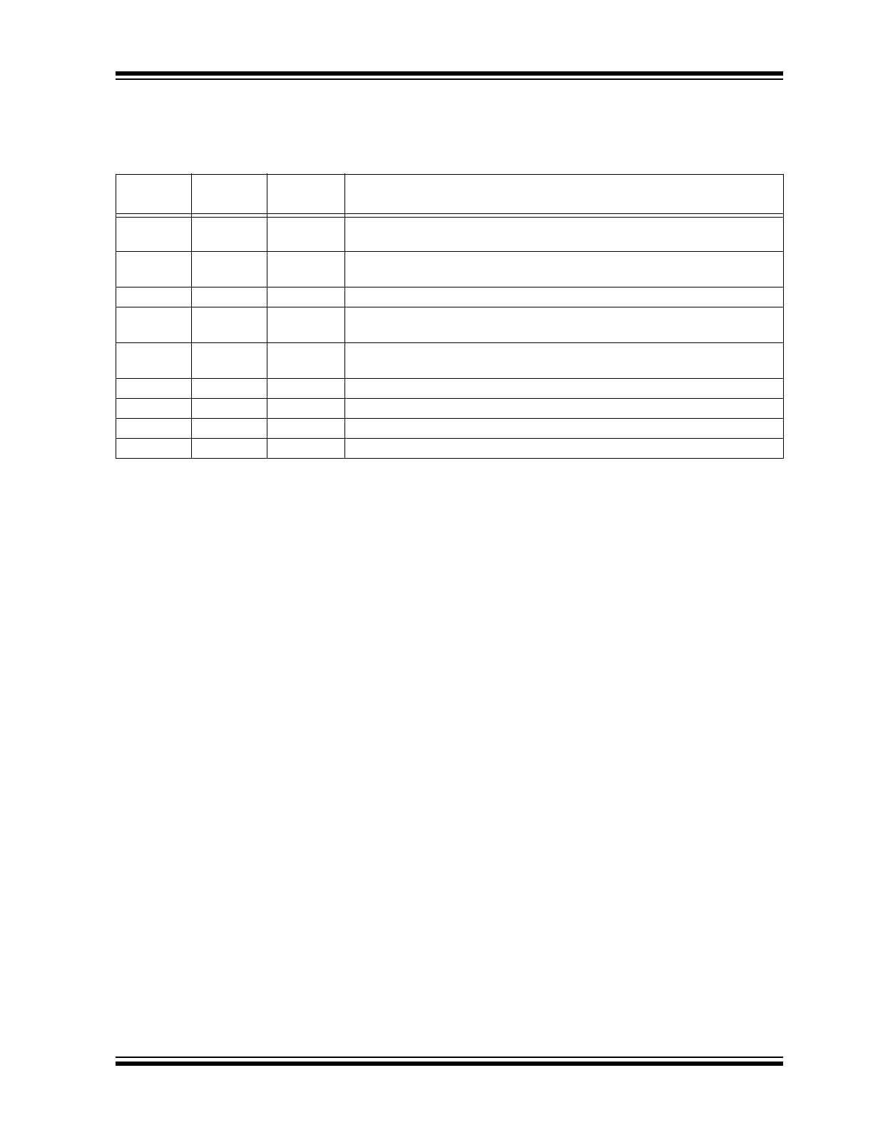
3.0
PIN DESCRIPTIONS
The descriptions of the pins are listed in
Table 3-1
.
3.1
Enable Pin (EN)
The EN pin is a logic-level input used to enable or
disable device switching. Device has low quiescent
current while disabled. A logic high (>75%
of V
IN
) will
enable the regulator output. A logic low (<20% of V
IN
)
will ensure that the regulator is disabled.
3.2
Feedback Voltage Pin (V
FB
)
The V
FB
pin is used to regulate the voltage across the
R
SET
sense resistor to 120 mV, to keep the output LED
current in regulation.
3.3
Unconnected Pin (NC)
This pin is unconnected.
3.4
Output Voltage Power Pin (V
OUT
)
High current flows through the integrated P-Channel
and out of this pin to the output capacitor, LED load and
R
SET
sense resistor. The output voltage must be
filtered using a 4.7 to 20 µF X7R or X5R ceramic
capacitor. The value of the output capacitor depends
on the load current.
3.5
Switch Node Pin (SW)
Connect the inductor from the input voltage to the SW
pin. The SW pin carries inductor current and can be as
high as 1.6 A typical peak value. The integrated
N-Channel switch drain and integrated P-Channel
switch source are internally connected at the SW node.
3.6
Power Ground (P
GND
) and Signal
Ground Pins (S
GND
)
The power ground pins are used as a return for the
high-current N-Channel switch.
The signal ground pin is used as a return for the
integrated V
FB
and error amplifier.
The length of the trace from input cap return, output
cap return and P
GND
and S
GND
should be made as
short as possible to minimize noise on the ground pins.
The S
GND
and P
GND
pins are connected externally.
3.7
Power Supply Input Voltage Pin
(V
IN
)
Connect the input voltage source to V
IN
. The input
source should be decoupled to GND with a 4.7 µF
minimum capacitor.
3.8
Exposed Thermal Pad (EP)
There is no internal electrical connection between the
Exposed Thermal Pad (EP) and the P
GND
and S
GND
pins. They must be connected to the same potential on
the Printed Circuit Board (PCB).
TABLE 3-1:
PIN FUNCTION TABLE
MCP1643
2 x 3 DFN
MCP1643
MSOP
Symbol
Description
1
1
EN
Enable pin. The logic high enables the operation. Do not allow this pin to
float.
2
2
V
FB
Reference Voltage pin. Connect to the V
FB
pin, the
R
SET
(LED current set
resistor), and the cathode of the LED load.
3
3
NC
Unconnected pin
4
4
V
OUT
Boost Converter Output pin. Connect to this pin the anode of the LED load.
An output filter capacitor is required.
5
5
SW
Boost and Rectifier Switch Input pin. Connect the boost inductor between
SW and V
IN
.
6
6
P
GND
Power Ground Reference pin
7
7
S
GND
Signal Ground Reference pin
8
8
V
IN
Input Supply Voltage pin. A local bypass capacitor is required.
9
—
EP
Exposed Thermal Pad, must be connected to V
SS

MCP1643
DS20005208A-page 10
2013 Microchip Technology Inc.
NOTES: