
©2013 Silicon Storage Technology, Inc.
DS20005203A
06/13
1
SST39LF010/020/040 and SST39VF010/020/040
45 ns and B3KE EOL Supplemental Information
EOL Data Sheet
Description
The SST39LF010, SST39LF020, SST39LF040 and SST39VF010, SST39VF020, SST39VF040 are
128K x8, 256K x8 and 5124K x8 CMOS Multi-Purpose Flash (MPF) manufactured with SST’s proprie-
tary, high performance CMOS SuperFlash technology. The split-gate cell design and thick-oxide tun-
neling injector attain better reliability and manufacturability compared with alternate approaches. The
SST39LF010/020/040 devices write (Program or Erase) with a 3.0-3.6V power supply. The
SST39VF010/020/040 devices write with a 2.7-3.6V power supply. The devices conform to JEDEC
standard pinouts for x8 memories.
This document provides supplemental information about the 45 ns and B3KE package parts which are
End-of-Life (EOL). Except for the information provided herein, the EOL parts behave as described in
the SST39LF010/020/040 and SST39VF010/020/040 data sheet DS-20005023. See page 3 for spe-
cific part numbers.
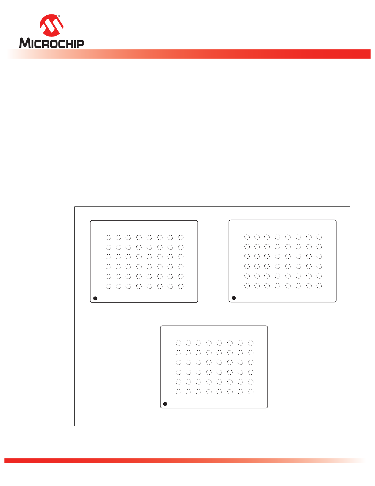
Pin Assignments
Figure 1:
Pin Assignment for 48-ball TFBGA (6mm x 8mm) for 1 Mbit, 2 Mbit, and 4 Mbit
1150 48-tfbga B3K P2.0
A B C D E F G H
SST39LF/VF010
6
5
4
3
2
1
TOP VIEW (balls facing down)
A14
A9
WE#
NC
A7
A3
A13
A8
NC
NC
NC
A4
A15
A11
NC
NC
A6
A2
A16
A12
NC
NC
A5
A1
NC
NC
DQ5
DQ2
DQ0
A0
NC
A10
NC
DQ3
NC
CE#
NC
DQ6
VDD
VDD
NC
OE#
VSS
DQ7
DQ4
NC
DQ1
VSS
1150 48-tfbga B3K P3.0
A B C D E F G H
SST39LF/VF020
6
5
4
3
2
1
TOP VIEW (balls facing down)
A14
A9
WE#
NC
A7
A3
A13
A8
NC
NC
NC
A4
A15
A11
NC
NC
A6
A2
A16
A12
NC
NC
A5
A1
A17
NC
DQ5
DQ2
DQ0
A0
NC
A10
NC
DQ3
NC
CE#
NC
DQ6
VDD
VDD
NC
OE#
VSS
DQ7
DQ4
NC
DQ1
VSS
1150 48-tfbga B3K P4.0
A B C D E F G H
SST39LF/VF040
6
5
4
3
2
1
TOP VIEW (balls facing down)
A14
A9
WE#
NC
A7
A3
A13
A8
NC
NC
A18
A4
A15
A11
NC
NC
A6
A2
A16
A12
NC
NC
A5
A1
A17
NC
DQ5
DQ2
DQ0
A0
NC
A10
NC
DQ3
NC
CE#
NC
DQ6
VDD
VDD
NC
OE#
VSS
DQ7
DQ4
NC
DQ1
VSS
©2013 Silicon Storage Technology, Inc.
DS20005203A
06/13
2
SST39LF010/020/040 and SST39VF010/020/040
45 ns and B3KE EOL Suplemental Information
EOL Data Sheet
AC Characteristics
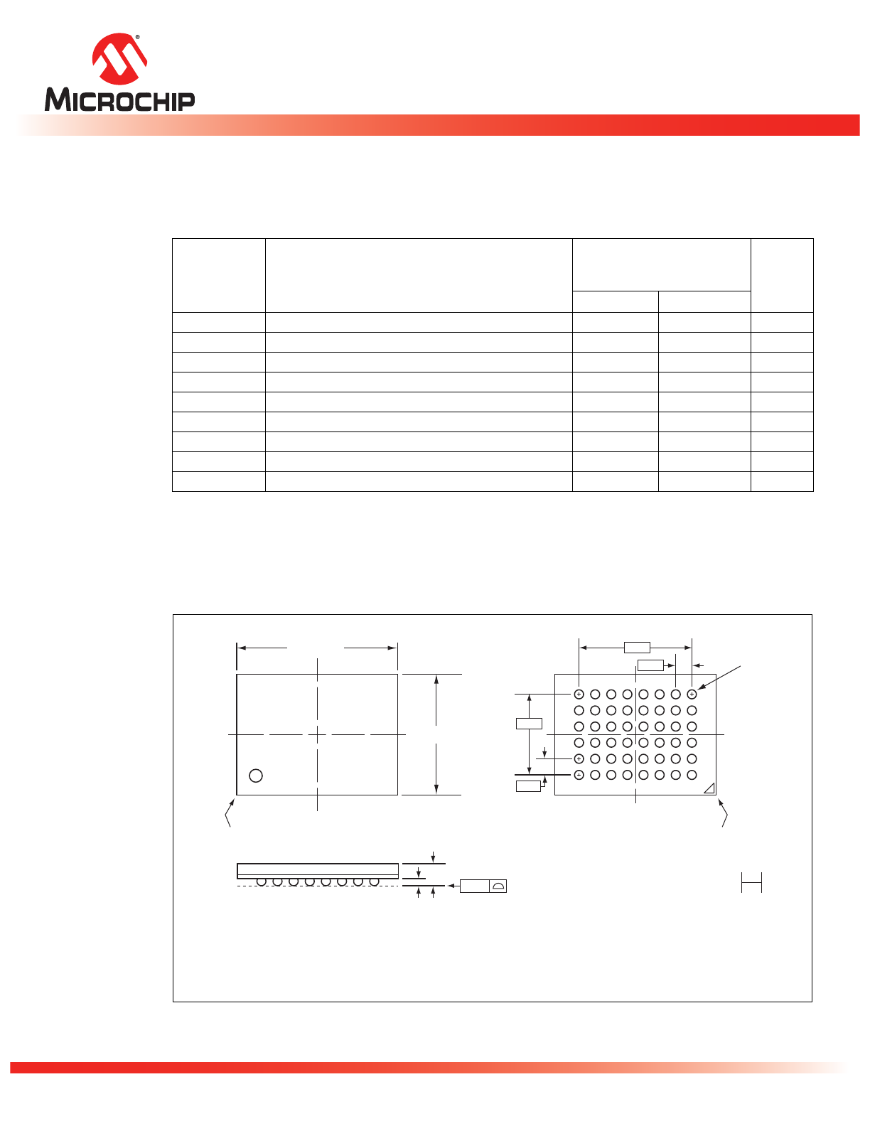
Packaging Diagram
Figure 2:
48-ball Thin-profile, Fine-pitch Ball Grid Array (TFBGA) 6mm x 8mm
SST Package Code: B3K
Table 1:
Read Cycle Timing Parameters V
DD
= 3.0-3.6V for SST39LF010/020/040
Symbol
Parameter
SST39LF010-45
SST39LF020-45
SST39LF040-45
Units
Min
Max
T
RC
Read Cycle Time
45
ns
T
CE
Chip Enable Access Time
45
ns
T
AA
Address Access Time
45
ns
T
OE
Output Enable Access Time
30
ns
T
CLZ
1
1. This parameter is measured only for initial qualification and after a design or process change that could affect this
parameter.
CE# Low to Active Output
0
ns
T
OLZ
1
OE# Low to Active Output
0
ns
T
CHZ
1
CE# High to High-Z Output
15
ns
T
OHZ
1
OE# High to High-Z Output
15
ns
T
OH
1
Output Hold from Address Change
0
ns
T1.2 25162
A1 CORNER
H G F E D C B A
A B C D E F G H
BOTTOM VIEW
TOP VIEW
SIDE VIEW
6
5
4
3
2
1
6
5
4
3
2
1
SEATING PLANE
0.35 ± 0.05
1.10 ± 0.10
0.12
6.00 ± 0.10
0.45 ± 0.05
(48X)
A1 CORNER
8.00 ± 0.10
0.80
4.00
0.80
5.60
48-tfbga-B3K-6x8-450mic-5
Note: 1. Complies with JEDEC Publication 95, MO-210, variant 'AB-1', although some dimensions may be more stringent.
2. All linear dimensions are in millimeters.
3. Coplanarity: 0.12 mm
4. Ball opening size is 0.38 mm (± 0.05 mm)
1mm
©2013 Silicon Storage Technology, Inc.
DS20005203A
06/13
3
SST39LF010/020/040 and SST39VF010/020/040
45 ns and B3KE EOL Suplemental Information
EOL Data Sheet
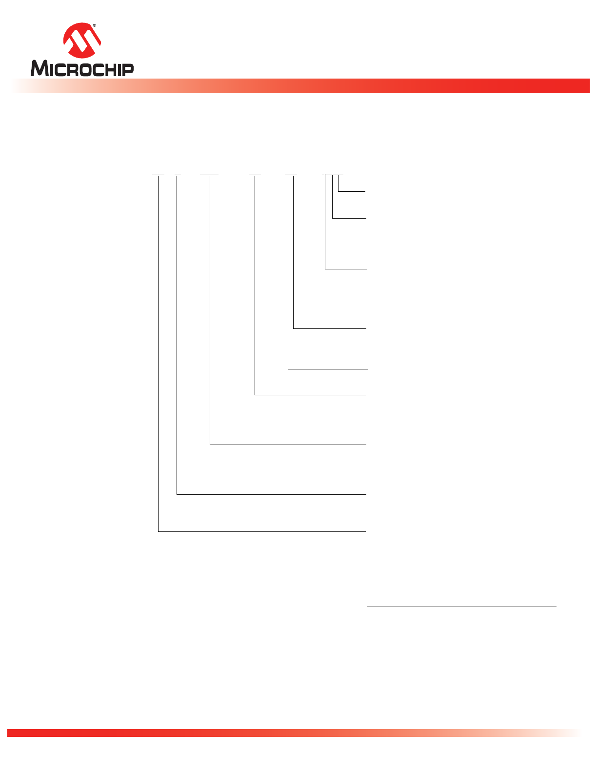
Product Ordering Information
SST
39
VF
010
-
45
-
4C
-
NHE
XX XX
XXX
- XX - XX
-
XXX
Environmental Attribute
E
1
= non-Pb
Package Modifier
H = 32 leads
K = 48 balls
M = 34 balls (54 possible positions)
Package Type
B3 = TFBGA (0.8mm pitch, 6mm x 8mm)
N = PLCC
M = WFBGA (0.5mm pitch, 4mm x 6mm)
W = TSOP (type 1, die up, 8mm x 14mm)
Temperature Range
C = Commercial = 0°C to +70°C
I = Industrial = -40°C to +85°C
Minimum Endurance
4 = 10,000 cycles
Read Access Speed
45 = 45 ns
55 = 55 ns
70 = 70 ns
Device Density
040 = 4 Mbit
020 = 2 Mbit
010 = 1 Mbit
Voltage
L = 3.0-3.6V
V = 2.7-3.6V
Product Series
39 = Multi-Purpose Flash
1. Environmental suffix “E” denotes non-Pb solder.
SST non-Pb solder devices are RoHS compliant.

©2013 Silicon Storage Technology, Inc.
DS20005203A
06/13
4
SST39LF010/020/040 and SST39VF010/020/040
45 ns and B3KE EOL Suplemental Information
EOL Data Sheet
Valid combinations for SST39LF010
SST39LF010-45-4C-NHE
SST39LF010-45-4C-WHE
SST39LF010-45-4C-B3KE
SST39LF010-45-4C-MME
Valid combinations for SST39VF010
SST39VF010-70-4C-B3KE
SST39VF010-70-4I-B3KE
Valid combinations for SST39LF020
SST39LF020-45-4C-NHE
SST39LF020-45-4C-WHE
SST39LF020-45-4C-B3KE
SST39LF020-45-4C-MME
Valid combinations for SST39VF020
SST39VF020-70-4C-B3KE
SST39VF020-70-4I-B3KE
Valid combinations for SST39LF040
SST39LF040-45-4C-NHE
SST39LF040-45-4C-WHE
SST39LF040-45-4C-B3KE
Valid combinations for SST39VF040
SST39VF040-70-4C-B3KE
SST39VF040-70-4I-B3KE
Note:
Valid combinations are those products in mass production or will be in mass production. Consult your SST
sales representative to confirm availability of valid combinations and to determine availability of new combi-
nations.
©2013 Silicon Storage Technology, Inc.
DS20005203A
06/13
5
SST39LF010/020/040 and SST39VF010/020/040
45 ns and B3KE EOL Suplemental Information
EOL Data Sheet
Table 2:
Revision History
Revision
Description
Date
A
•
EOL document for 45 ns parts and B3KE parts
Jun 2013
© 2013 Silicon Storage Technology, Inc–a Microchip Technology Company. All rights reserved.
SST, Silicon Storage Technology, the SST logo, SuperFlash, MTP, and FlashFlex are registered trademarks of Silicon Storage Tech-
nology, Inc. MPF, SQI, Serial Quad I/O, and Z-Scale are trademarks of Silicon Storage Technology, Inc. All other trademarks and
registered trademarks mentioned herein are the property of their respective owners.
Specifications are subject to change without notice. Refer to www.microchip.com for the most recent documentation. For the most current
package drawings, please see the Packaging Specification located at http://www.microchip.com/packaging.
Memory sizes denote raw storage capacity; actual usable capacity may be less.
SST makes no warranty for the use of its products other than those expressly contained in the Standard Terms and Conditions of
Sale.
For sales office locations and information, please see www.microchip.com.
Silicon Storage Technology, Inc.
A Microchip Technology Company
www.microchip.com
ISBN:978-1-62077-293-5