

©2014 Silicon Storage Technology, Inc.
DS20005086B
11/14
Data Sheet
www.microchip.com
Features
• LPC Interface Flash
– SST49LF080A: 1024K x8 (8 Mbit)
• Conforms to Intel LPC Interface Specification 1.0
• Flexible Erase Capability
– Uniform 4 KByte Sectors
– Uniform 64 KByte overlay blocks
– 64 KByte Top Boot Block protection
– Chip-Erase for PP Mode Only
• Single 3.0-3.6V Read and Write Operations
• Superior Reliability
– Endurance: 100,000 Cycles (typical)
– Greater than 100 years Data Retention
• Low Power Consumption
– Active Read Current: 6 mA (typical)
– Standby Current: 10 µA (typical)
• Fast Sector-Erase/Byte-Program Operation
– Sector-Erase Time: 18 ms (typical)
– Block-Erase Time: 18 ms (typical)
– Chip-Erase Time: 70 ms (typical)
– Byte-Program Time: 14 µs (typical)
– Chip Rewrite Time: 16 seconds (typical)
– Single-pulse Program or Erase
– Internal timing generation
• Two Operational Modes
– Low Pin Count (LPC) Interface mode for
in-system operation
– Parallel Programming (PP) Mode for fast production pro-
gramming
• LPC Interface Mode
– 5-signal communication interface supporting byte Read
and Write
– 33 MHz clock frequency operation
– WP# and TBL# pins provide hardware write protect for
entire chip and/or top boot block
– Standard SDP Command Set
– Data# Polling and Toggle Bit for End-of-Write detection
– 5 GPI pins for system design flexibility
– 4 ID pins for multi-chip selection
• Parallel Programming (PP) Mode
– 11-pin multiplexed address and 8-pin data
I/O interface
– Supports fast programming In-System on
programmer equipment
• CMOS and PCI I/O Compatibility
• Packages Available
– 32-lead PLCC
– 32-lead TSOP (8mm x 14mm)
• All non-Pb (lead-free) devices are RoHS compliant
8 Mbit LPC Flash
SST49LF080A
The SST49LF080A flash memory device is designed to interface with the LPC
bus for PC and Internet Appliance application in compliance with Intel Low Pin
Count (LPC) Interface Specification 1.0. Two interface modes are supported: LPC
mode for in-system operations and Parallel Programming (PP) mode to interface
with programming equipment. The SST49LF080A flash memory device is manu-
factured with proprietary, high-performance SuperFlash® Technology. The split-
gate cell design and thick-oxide tunneling injector attain better reliability and man-
ufacturability compared with alternate approaches

©2014 Silicon Storage Technology, Inc.
DS20005086B
11/14
2
8 Mbit LPC Flash
SST49LF080A
Data Sheet
Product Description
SST49LF080A flash memory device is designed to interface with the LPC bus for PC and Internet
Appliance application in compliance with Intel Low Pin Count (LPC) Interface Specification 1.0. Two
interface modes are supported: LPC mode for in-system operations and Parallel Programming (PP)
mode to interface with programming equipment.
SST49LF080A flash memory device is manufactured with proprietary, high-performance SuperFlash
Technology. The split-gate cell design and thick-oxide tunneling injector attain better reliability and
manufacturability compared with alternate approaches. The SST49LF080A device significantly
improves performance and reliability, while lowering power consumption. The SST49LF080A device
writes (Program or Erase) with a single 3.0-3.6V power supply. It uses less energy during Erase and
Program than alternative flash memory technologies. The total energy consumed is a function of the
applied voltage, current and time of application. For any give voltage range, the SuperFlash technology
uses less current to program and has a shorter erase time; the total energy consumed during any
Erase or Program operation is less than alternative flash memory technologies. The SST49LF080A
product provides a maximum Byte-Program time of 20 µsec. The entire memory can be erased and
programmed byte-by-byte typically in 16 seconds when using status detection features such as Toggle
Bit or Data# Polling to indicate the completion of Program operation. The SuperFlash technology pro-
vides fixed Erase and Program time, independent of the number of Erase/Program cycles that have
performed. Therefore the system software or hardware does not have to be calibrated or correlated to
the cumulative number of Erase cycles as is necessary with alternative flash memory technologies,
whose Erase and Program time increase with accumulated Erase/Program cycles.
To meet high density, surface mount requirements, the SST49LF080A device is offered in 32-lead
TSOP and 32-lead PLCC packages. See Figures 2 and 3 for pin assignments and Table 1 for pin
descriptions.
©2014 Silicon Storage Technology, Inc.
DS20005086B
11/14
3
8 Mbit LPC Flash
SST49LF080A
Data Sheet
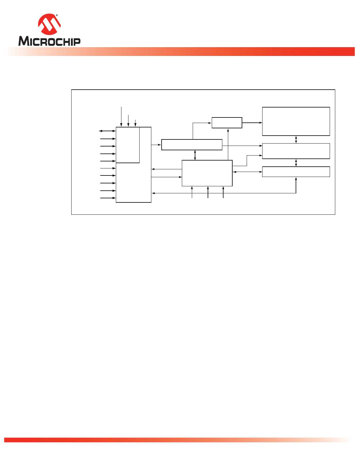
Functional Block Diagram
Figure 1: Functional Block Diagram
1235 B1.0
Y-Decoder
I/O Buffers and Data Latches
Address Buffers Latches
X-Decoder
SuperFlash
Memory
Control Logic
LCLK
RST#
CE#
MODE
GPI[4:0]
Programmer
Interface
WP#
TBL#
INIT#
ID[3:0]
LFRAME#
R/C#
OE#
WE#
A[10:0]
DQ[7:0]
LAD[3:0]
LPC
Interface
©2014 Silicon Storage Technology, Inc.
DS20005086B
11/14
4
8 Mbit LPC Flash
SST49LF080A
Data Sheet
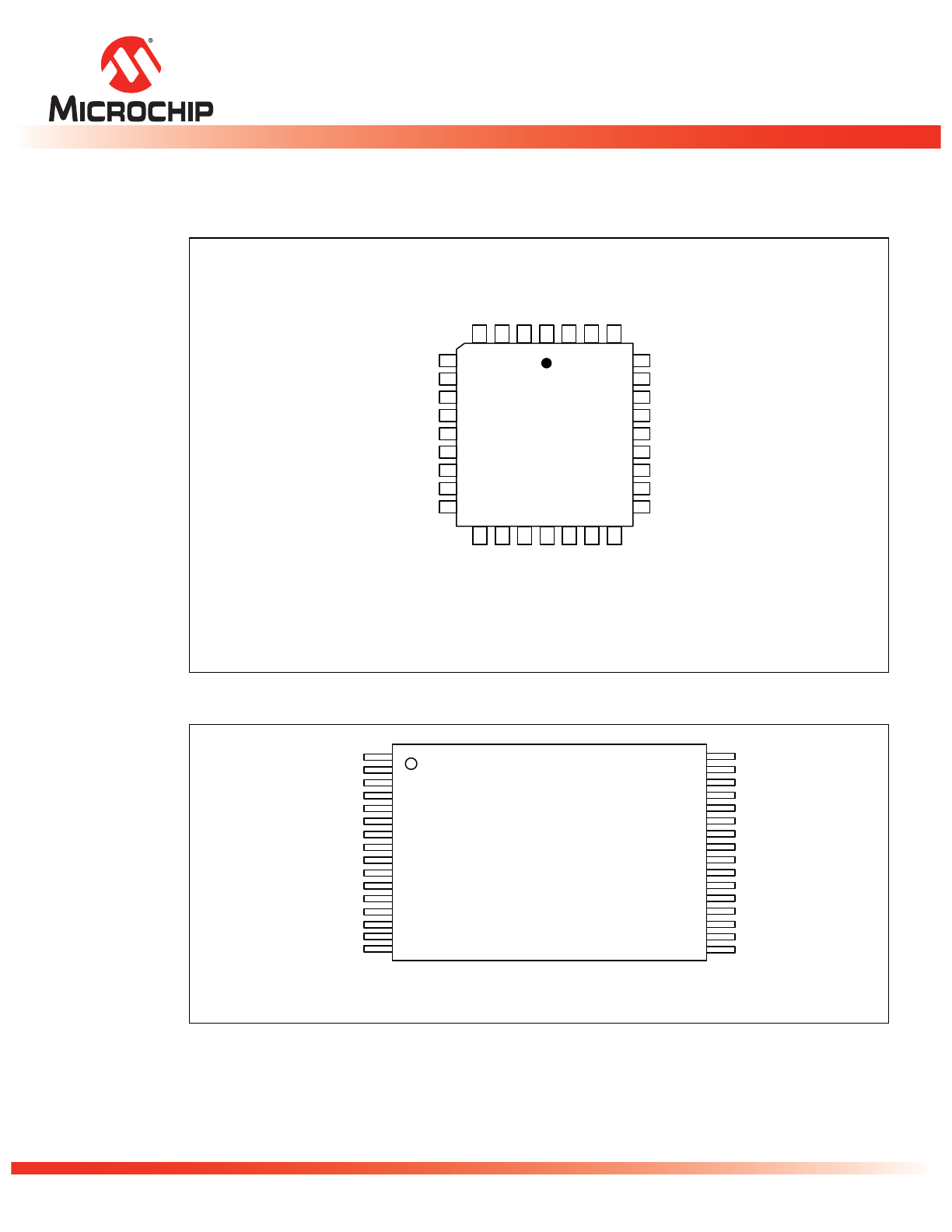
Pin Assignments
Figure 2: Pin Assignments for 32-lead PLCC
Figure 3: Pin Assignments for 32-lead TSOP (8mm x 14mm)
5
6
7
8
9
10
11
12
13
29
28
27
26
25
24
23
22
21
A7(GPI1)
A6 (GPI0)
A5 (WP#)
A4 (TBL#)
A3 (ID3)
A2 (ID2)
A1 (ID1)
A0 (ID0)
DQ0 (LAD0)
MODE (MODE)
NC (CE#)
NC
NC
VDD (VDD)
OE# (INIT#)
WE# (LFRAME#)
NC
DQ7 (RES)
4
3
2
1
32
31 30
A8
(GPI2)
A9
(GPI3)
RST#
(RST#)
NC
V
DD
(V
DD
)
R/C#
(LCLK)
A10
(GPI4)
32-lead PLCC
Top View
1235 32-plcc P1.0
14
15
16
17 18
19
20
DQ1
(LAD1)
DQ2
(LAD2)
V
SS
(V
SS
)
DQ3
(LAD3)
DQ4
(RES)
DQ5
(RES)
DQ6
(RES)
( ) Designates LPC Mode
NC
NC
NC
NC (CE#)
MODE (MODE)
A10 (GPI4)
R/C# (LCLK)
VDD (VDD)
NC
RST# (RST#)
A9 (GPI3)
A8 (GPI2)
A7 (GPI1)
A6 (GPI0)
A5 (WP#)
A4 (TBL#)
1
2
3
4
5
6
7
8
9
10
11
12
13
14
15
16
OE# (INIT#)
WE# (LFRAME#)
VDD (VDD)
DQ7 (RES)
DQ6 (RES)
DQ5 (RES)
DQ4 (RES)
DQ3 (LAD3)
VSS (VSS)
DQ2 (LAD2)
DQ1 (LAD1)
DQ0 (LAD0)
A0 (ID0)
A1 (ID1)
A2 (ID2)
A3 (ID3)
32
31
30
29
28
27
26
25
24
23
22
21
20
19
18
17
1235 32-tsop P2.0
Standard Pinout
Top View
Die Up
( ) Designates LPC Mode
©2014 Silicon Storage Technology, Inc.
DS20005086B
11/14
5
8 Mbit LPC Flash
SST49LF080A
Data Sheet
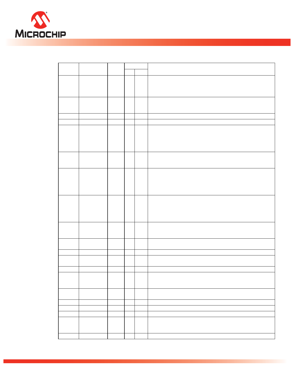
Table 1: Pin Description
Symbol
Pin Name
Type
1
Interface
Functions
PP
LPC
A
10
-A
0
Address
I
X
Inputs for low-order addresses during Read and Write operations.
Addresses are internally latched during a Write cycle. For the pro-
gramming interface, these addresses are latched by R/C# and share
the same pins as the high-order address inputs.
DQ
7
-DQ
0
Data
I/O
X
To output data during Read cycles and receive input data during
Write cycles. Data is internally latched during a Write cycle. The out-
puts are in tri-state when OE# is high.
OE#
Output Enable
I
X
To gate the data output buffers.
WE#
Write Enable
I
X
To control the Write operations.
MODE
Interface
Mode Select
I
X
X
This pin determines which interface is operational. When held high,
programmer mode is enabled and when held low, LPC mode is
enabled. This pin must be setup at power-up or before return from
reset and not change during device operation. This pin must be held
high (V
IH
) for PP mode and low (V
IL
) for LPC mode.
INIT#
Initialize
I
X
This is the second reset pin for in-system use. This pin is inter-
nally combined with the RST# pin; If this pin or RST# pin is driven
low, identical operation is exhibited.
ID[3:0]
Identification
Inputs
I
X
These four pins are part of the mechanism that allows multiple parts to
be attached to the same bus. The strapping of these pins is used to
identify the component.The boot device must have ID[3:0]=0000 for all
subsequent devices should use sequential up-count strapping. These
pins are internally pulled-down with a resistor between 20-100 K
GPI[4:0]
General
Purpose
Inputs
I
X
These individual inputs can be used for additional board flexibility. The
state of these pins can be read through LPC registers. These inputs
should be at their desired state before the start of the PCI clock cycle dur-
ing which the read is attempted, and should remain in place until the end
of the Read cycle. Unused GPI pins must not be floated.
TBL#
Top Block
Lock
I
X
When low, prevents programming to the boot block sectors at top of
memory. When TBL# is high it disables hardware write protection for
the top block sectors. This pin cannot be left unconnected.
LAD[3:0] Address and
Data
I/O
X
To provide LPC control signals, as well as addresses and Command
Inputs/Outputs data.
LCLK
Clock
I
X
To provide a clock input to the control unit
LFRAME# Frame
I
X
To indicate start of a data transfer operation; also used to abort
an LPC cycle in progress.
RST#
Reset
I
X
X
To reset the operation of the device
WP#
Write Protect
I
X
When low, prevents programming to all but the highest addressable
blocks. When WP# is high it disables hardware write protection for
these blocks. This pin cannot be left unconnected.
R/C#
Row/Column
Select
I
X
Select for the Programming interface, this pin determines whether the address
pins are pointing to the row addresses, or to the column addresses.
RES
Reserved
X
These pins must be left unconnected.
V
DD
Power Supply
PWR
X
X
To provide power supply (3.0-3.6V)
V
SS
Ground
PWR
X
X
Circuit ground (0V reference)
CE#
Chip Enable
I
X
This signal must be asserted to select the device. When CE# is low,
the device is enabled. When CE# is high, the device is placed in low
power standby mode.
NC
No Connection
I
X
X
Unconnected pins.
T1.0 25026
1. I=Input, O=Output
©2014 Silicon Storage Technology, Inc.
DS20005086B
11/14
6
8 Mbit LPC Flash
SST49LF080A
Data Sheet
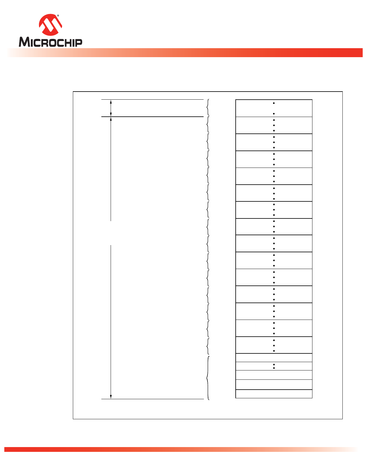
Device Memory Maps
Figure 4: Device Memory Map
0FFFFFH
0F0000H
0EFFFFH
0E0000H
0DFFFFH
0D0000H
0CFFFFH
0C0000H
0BFFFFH
0B0000H
0AFFFFH
0A0000H
09FFFFH
090000H
08FFFFH
080000H
07FFFFH
070000H
06FFFFH
060000H
05FFFFH
050000H
04FFFFH
040000H
03FFFFH
030000H
02FFFFH
020000H
01FFFFH
010000H
00FFFFH
Block 7
Block 8
Block 6
Block 5
Block 4
Block 3
Block 2
Block 1
Block 15
Block 14
Block 13
Block 12
Block 11
Block 10
Block 9
Block 0
(64 KByte)
1235 F03.0
WP# for
Block 0 14
TBL#
4 KByte Sector 1
4 KByte Sector 2
4 KByte Sector 15
4 KByte Sector 0
Boot Block
002000H
001000H
000000H
©2014 Silicon Storage Technology, Inc.
DS20005086B
11/14
7
8 Mbit LPC Flash
SST49LF080A
Data Sheet
Design Considerations
SST recommends a high frequency 0.1 µF ceramic capacitor to be placed as close as possible
between V
DD
and V
SS
less than 1 cm away from the V
DD
pin of the device. Additionally, a low fre-
quency 4.7 µF electrolytic capacitor from V
DD
to V
SS
should be placed within 5 cm of the V
DD
pin. If you
use a socket for programming purposes add an additional 1-10 µF next to each socket.
Product Identification
The Product Identification mode identifies the device as the SST49LF080A and manufacturer as SST.
Mode Selection
The SST49LF080A flash memory devices can operate in two distinct interface modes: the LPC mode
and the Parallel Programming (PP) mode. The mode pin is used to set the interface mode selection. If
the mode pin is set to logic High, the device is in PP mode. If the mode pin is set Low, the device is in
the LPC mode. The mode selection pin must be configured prior to device operation. The mode pin is
internally pulled down if the pin is left unconnected. In LPC mode, the device is configured to its host
using standard LPC interface protocol. Communication between Host and the SST49LF080A occurs
via the 4-bit I/O communication signals, LAD [3:0] and LFRAME#. In PP mode, the device is pro-
grammed via an 11-bit address and an 8-bit data I/O parallel signals. The address inputs are multi-
plexed in row and column selected by control signal R/C# pin. The row addresses are mapped to the
lower internal addresses (A
10-0
), and the column addresses are mapped to the higher internal
addresses (A
MS-11
). See Figure 4, the Device Memory Map, for address assignments.
Table 2: Product Identification
Address
Data
Manufacturer’s ID
0000H
BFH
Device ID
SST49LF080A
0001H
5BH
T2.0 25026
©2014 Silicon Storage Technology, Inc.
DS20005086B
11/14
8
8 Mbit LPC Flash
SST49LF080A
Data Sheet
LPC Mode
Device Operation
The LPC mode uses a 5-signal communication interface, a 4-bit address/data bus, LAD[3:0], and a
control line, LFRAME#, to control operations of the SST49LF080A. Cycle type operations such as
Memory Read and Memory Write are defined in Intel Low Pin Count Interface Specification, Revision
1.0. JEDEC Standard SDP (Software Data Protection) Program and Erase commands sequences are
incorporated into the standard LPC memory cycles. See Figures 7 through 12 for command
sequences.
LPC signals are transmitted via the 4-bit Address/Data bus (LAD[3:0]), and follow a particular
sequence, depending on whether they are Read or Write operations. LPC memory Read and Write
cycle is defined in Tables 5 and 6.
Both LPC Read and Write operations start in a similar way as shown in Figures 5 and 6. The host
(which is the term used here to describe the device driving the memory) asserts LFRAME# for two or
more clocks and drives a start value on the LAD[3:0] bus.
At the beginning of an operation, the host may hold the LFRAME# active for several clock cycles, and
even change the Start value. The LAD[3:0] bus is latched every rising edge of the clock. On the cycle
in which LFRAME# goes inactive, the last latched value is taken as the Start value. CE# must be
asserted one cycle before the start cycle to select the SST49LF080A for Read and Write operations.
Once the SST49LF080A identifies the operation as valid (a start value of all zeros), it next expects a
nibble that indicates whether this is a memory Read or Write cycle. Once this is received, the device is
now ready for the Address cycles. The LPC protocol supports a 32-bit address phase. The
SST49LF080A encodes ID and register space access in the address field. See Table 3 for address bits
definition.
For Write operation the Data cycle will follow the Address cycle, and for Read operation TAR and
SYNC cycles occur between the Address and Data cycles. At the end of every operation, the control of
the bus must be returned to the host by a 2-clock TAR cycle.
Table 3: Address bits definition
A
31
: A
25
1
1. The top 32MByte address range FFFF FFFFH to FE00 0000H and the bottom 128 KByte memory access address
000F FFFFH to 000E 0000H are decoded.
A
24
:A
23
A
22
A
21
: A
20
A
19
:A
0
1111 111b or 0000 000b
ID[3:2]
2
2. See Table 7 for multiple device selection configuration
1 = Memory Access
0 = Register access
ID[1:0]
2
Device Memory address
T3.1 25026

©2014 Silicon Storage Technology, Inc.
DS20005086B
11/14
9
8 Mbit LPC Flash
SST49LF080A
Data Sheet
CE#
The CE# pin, enables and disables the SST49LF080A, controlling read and write access of the device.
To enable the SST49LF080A, the CE# pin must be driven low one clock cycle prior to LFRAME# being
driven low. The device will enter standby mode when internal Write operations are completed and CE#
is high.
LFRAME#
The LFRAME# signifies the start of a (frame) bus cycle or the termination of an undesired cycle.
Asserting LFRAME# for one or more clock cycle and driving a valid START value on LAD[3:0] will initi-
ate device operation. The device will enter standby mode when internal operations are completed and
LFRAME# is high.
TBL#, WP#
The Top Boot Lock (TBL#) and Write Protect (WP#) pins are provided for hardware write protection of
device memory. The TBL# pin is used to Write-Protect 16 boot sectors (64 KByte) at the highest mem-
ory address range for the SST49LF080A. The WP# pin write protects the remaining sectors in the
flash memory.
An active low signal at the TBL# pin prevents Program and Erase operations of the top boot sectors.
When TBL# pin is held high, the write protection of the top boot sectors is disabled. The WP# pin
serves the same function for the remaining sectors of the device memory. The TBL# and WP# pins
write protection functions operate independently of one another.
Both TBL# and WP# pins must be set to their required protection states prior to starting a Program or
Erase operation. A logic level change occurring at the TBL# or WP# pin during a Program or Erase
operation could cause unpredictable results.
©2014 Silicon Storage Technology, Inc.
DS20005086B
11/14
10
8 Mbit LPC Flash
SST49LF080A
Data Sheet
INIT#, RST#
A V
IL
on INIT# or RST# pin initiates a device reset. INIT# and RST# pins have the same function
internally. It is required to drive INIT# or RST# pins low during a system reset to ensure proper
CPU initialization. During a Read operation, driving INIT# or RST# pins low deselects the device
and places the output drivers, LAD[3:0], in a high-impedance state. The reset signal must be held
low for a minimal duration of time T
RSTP
. A reset latency will occur if a reset procedure is performed
during a Program or Erase operation. See Table 19, Reset Timing Parameters for more informa-
tion. A device reset during an active Program or Erase will abort the operation and memory con-
tents may become invalid due to data being altered or corrupted from an incomplete Erase or
Program operation.
System Memory Mapping
The LPC interface protocol has address length of 32-bit or 4 GByte. The SST49LF080A will
respond to addresses in the range as specified in Table 4.
Refer to “Multiple Device Selection” section for more detail on strapping multiple SST49LF080A
devices to increase memory densities in a system and “Registers” section on valid register
addresses.
Table 4: Address Decoding Range
ID Strapping
Device Access
Address Range
Memory Size
Device #0 - 3
Memory Access
FFFF FFFFH : FFC0 0000H
4 MByte
Register Access
FFBF FFFFH : FF80 0000H
4 MByte
Device #4 - 7
Memory Access
FF7F FFFFH : FF40 0000H
4 MByte
Register Access
FF3F FFFFH : FF00 0000H
4 MByte
Device #8 - 11
Memory Access
FEFF FFFFH : FEC0 0000H
4 MByte
Register Access
FEBF FFFFH : FE80 0000H
4 MByte
Device #12 - 15
Memory Access
FE7F FFFFH : FE40 0000H
4 MByte
Register Access
FE3F FFFFH : FE00 0000H
4 MByte
Device #0
1
1. For device #0 (Boot Device), SST49LF080A decodes the physical addresses of the top 2 blocks (including Boot
Block) both at
system memory ranges FFFF FFFFH to FFFE 0000H and 000F FFFFH to 000E 0000H.
Memory Access
000F FFFFH : 000E 0000H
128 KByte
T4.0 25026