

©2013 Silicon Storage Technology, Inc.
DS20005054C
04/13
Data Sheet
www.microchip.com
Features
• Single Voltage Read and Write Operations
– 2.7-3.6V
• Serial Interface Architecture
– SPI Compatible: Mode 0 and Mode 3
• High Speed Clock Frequency
– Up to 80 MHz
• Superior Reliability
– Endurance: 100,000 Cycles
– Greater than 100 years Data Retention
• Low Power Consumption:
– Active Read Current: 10 mA (typical)
– Standby Current: 5 µA (typical)
• Flexible Erase Capability
– Uniform 4 KByte sectors
– Uniform 32 KByte overlay blocks
– Uniform 64 KByte overlay blocks
• Fast Erase and Byte-Program:
– Chip-Erase Time: 35 ms (typical)
– Sector-/Block-Erase Time: 18 ms (typical)
– Byte-Program Time: 7 µs (typical)
• Auto Address Increment (AAI) Programming
– Decrease total chip programming time over Byte-Pro-
gram operations
• End-of-Write Detection
– Software polling the BUSY bit in Status Register
– Busy Status readout on SO pin in AAI Mode
• Hold Pin (HOLD#)
– Suspends a serial sequence to the memory
without deselecting the device
• Write Protection (WP#)
– Enables/Disables the Lock-Down function of the status
register
• Software Write Protection
– Write protection through Block-Protection bits in status
register
• Temperature Range
– Commercial: 0°C to +70°C
– Industrial: -40°C to +85°C
• Packages Available
– 8-lead SOIC (150 mils)
– 8-contact WSON (6mm x 5mm)
– 8-contact USON (3mm x 2mm)
• All non-Pb (lead-free) devices are RoHS compliant
2 Mbit SPI Serial Flash
SST25VF020B
The 25 series Serial Flash family features a four-wire, SPI compatible interface
that allows for a low pin-count package which occupies less board space and ulti-
mately lowers total system costs. The SST25VF020B devices are enhanced with
improved operating frequency and even lower power consumption.
SST25VF020B SPI serial flash memories are manufactured with SST proprietary,
high performance CMOS SuperFlash technology. The split-gate cell design and
thick-oxide tunneling injector attain better reliability and manufacturability com-
pared with alternate approaches.

©2013 Silicon Storage Technology, Inc.
DS20005054C
04/13
2
2 Mbit SPI Serial Flash
SST25VF020B
Data Sheet
Product Description
The 25 series Serial Flash family features a four-wire, SPI-compatible interface that allows for a low
pin-count package which occupies less board space and ultimately lowers total system costs. The
SST25VF020B devices are enhanced with improved operating frequency and even lower power con-
sumption. SST25VF020B SPI serial flash memories are manufactured with SST proprietary, high-per-
formance CMOS SuperFlash technology. The split-gate cell design and thick-oxide tunneling injector
attain better reliability and manufacturability compared with alternate approaches.
The SST25VF020B devices significantly improve performance and reliability, while lowering power
consumption. The devices write (Program or Erase) with a single power supply of 2.7-3.6V for
SST25VF020B. The total energy consumed is a function of the applied voltage, current, and time of
application. Since for any given voltage range, the SuperFlash technology uses less current to pro-
gram and has a shorter erase time, the total energy consumed during any Erase or Program operation
is less than alternative flash memory technologies.
The SST25VF020B device is offered in 8-lead SOIC (150 mils) 8-contact WSON (6mm x 5mm), and 8-
contact USON (3mm x 2mm) packages. See Figure 2 for pin assignments.
©2013 Silicon Storage Technology, Inc.
DS20005054C
04/13
3
2 Mbit SPI Serial Flash
SST25VF020B
Data Sheet
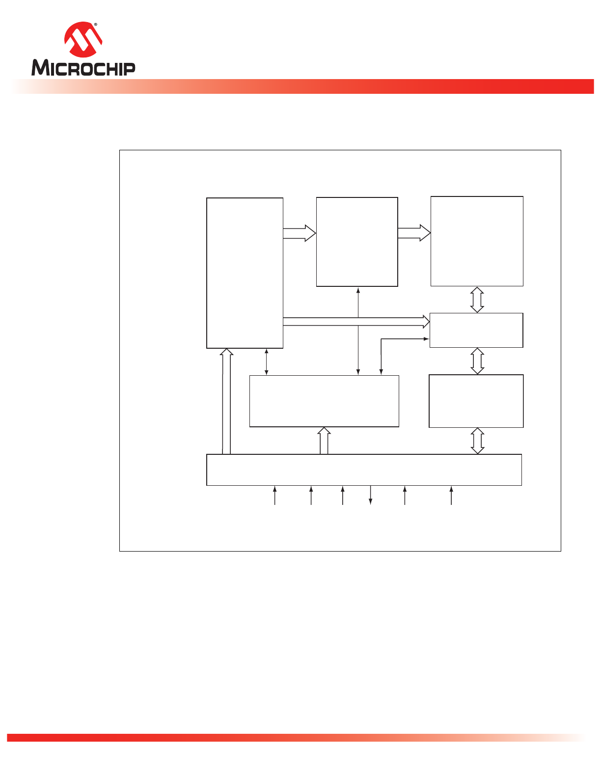
Functional Block Diagram
Figure 1: Functional Block Diagram
1417 B1.0
I/O Buffers
and
Data Latches
SuperFlash
Memory
X - Decoder
Control Logic
Address
Buffers
and
Latches
CE#
Y - Decoder
SCK
SI
SO
WP#
HOLD#
Serial Interface
©2013 Silicon Storage Technology, Inc.
DS20005054C
04/13
4
2 Mbit SPI Serial Flash
SST25VF020B
Data Sheet
Pin Description
Figure 2: Pin Assignments
Table 1: Pin Description
Symbol
Pin Name
Functions
SCK
Serial Clock
To provide the timing of the serial interface.
Commands, addresses, or input data are latched on the rising edge of the clock
input, while output data is shifted out on the falling edge of the clock input.
SI
Serial Data Input
To transfer commands, addresses, or data serially into the device.
Inputs are latched on the rising edge of the serial clock.
SO
Serial Data Output To transfer data serially out of the device.
Data is shifted out on the falling edge of the serial clock.
Outputs Flash busy status during AAI Programming when reconfigured as RY/
BY# pin. See “Hardware End-of-Write Detection” on page 14 for details.
CE#
Chip Enable
The device is enabled by a high to low transition on CE#. CE# must remain low
for the duration of any command sequence.
WP#
Write Protect
The Write Protect (WP#) pin is used to enable/disable BPL bit in the status reg-
ister.
HOLD#
Hold
To temporarily stop serial communication with SPI flash memory without reset-
ting the device.
V
DD
Power Supply
To provide power supply voltage: 2.7-3.6V for SST25VF020B
V
SS
Ground
T1.0 25054
1
2
3
4
8
7
6
5
CE#
SO
WP#
VSS
VDD
HOLD#
SCK
SI
Top View
1417 08-soic S2A P1.0
8-Lead SOIC
1
2
3
4
8
7
6
5
CE#
SO
WP#
VSS
Top View
VDD
HOLD#
SCK
SI
1417 08-wson QA P2.0
8-Contact WSON
1
2
3
4
8
7
6
5
CE#
SO
WP#
VSS
Top View
VDD
HOLD#
SCK
SI
1417 08-uson Q3A P1.0
8-Contact USON
©2013 Silicon Storage Technology, Inc.
DS20005054C
04/13
5
2 Mbit SPI Serial Flash
SST25VF020B
Data Sheet
Memory Organization
The SST25VF020B SuperFlash memory array is organized in uniform 4 KByte erasable sectors with 32
KByte overlay blocks and 64 KByte overlay erasable blocks.
Device Operation
The SST25VF020B is accessed through the SPI (Serial Peripheral Interface) bus compatible protocol.
The SPI bus consist of four control lines; Chip Enable (CE#) is used to select the device, and data is
accessed through the Serial Data Input (SI), Serial Data Output (SO), and Serial Clock (SCK).
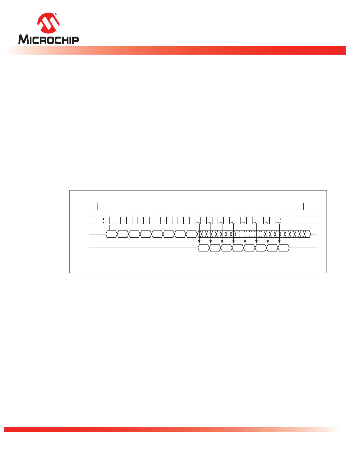
The SST25VF020B supports both Mode 0 (0,0) and Mode 3 (1,1) of SPI bus operations. The difference
between the two modes, as shown in Figure 3, is the state of the SCK signal when the bus master is in
Stand-by mode and no data is being transferred. The SCK signal is low for Mode 0 and SCK signal is
high for Mode 3. For both modes, the Serial Data In (SI) is sampled at the rising edge of the SCK clock
signal and the Serial Data Output (SO) is driven after the falling edge of the SCK clock signal.
Figure 3: SPI Protocol
1417 SPIprot.0
MODE 3
SCK
SI
SO
CE#
MODE 3
DON'T CARE
Bit 7 Bit 6 Bit 5 Bit 4 Bit 3 Bit 2 Bit 1 Bit 0
Bit 7 Bit 6 Bit 5 Bit 4 Bit 3 Bit 2 Bit 1 Bit 0
MODE 0
MODE 0
HIGH IMPEDANCE
MSB
MSB
©2013 Silicon Storage Technology, Inc.
DS20005054C
04/13
6
2 Mbit SPI Serial Flash
SST25VF020B
Data Sheet
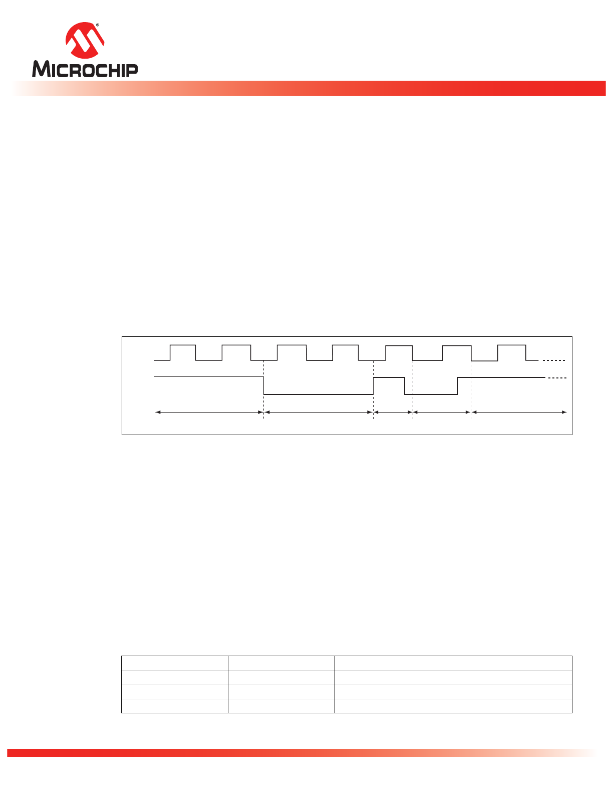
Hold Operation
The HOLD# pin is used to pause a serial sequence underway with the SPI flash memory without reset-
ting the clocking sequence. To activate the HOLD# mode, CE# must be in active low state. The HOLD#
mode begins when the SCK active low state coincides with the falling edge of the HOLD# signal. The
HOLD mode ends when the HOLD# signal’s rising edge coincides with the SCK active low state.
If the falling edge of the HOLD# signal does not coincide with the SCK active low state, then the device
enters Hold mode when the SCK next reaches the active low state. Similarly, if the rising edge of the
HOLD# signal does not coincide with the SCK active low state, then the device exits in Hold mode
when the SCK next reaches the active low state. See Figure 4 for Hold Condition waveform.
Once the device enters Hold mode, SO will be in high-impedance state while SI and SCK can be V
IL
or
V
IH.
If CE# is driven high during a Hold condition, the device returns to Standby mode. As long as HOLD#
signal is low, the memory remains in the Hold condition. To resume communication with the device,
HOLD# must be driven active high, and CE# must be driven active low. See Figure 4 for Hold timing.
Figure 4: Hold Condition Waveform
Write Protection
SST25VF020B provides software Write protection. The Write Protect pin (WP#) enables or disables
the lock-down function of the status register. The Block-Protection bits (BP1, BP0, and BPL) in the sta-
tus register, and the Top/Bottom Sector Protection Status bits (TSP and BSP) in Status Register 1, pro-
vide Write protection to the memory array and the status register. See Table 5 for the Block-Protection
description.
Write Protect Pin (WP#)
The Write Protect (WP#) pin enables the lock-down function of the BPL bit (bit 7) in the status register.
When WP# is driven low, the execution of the Write-Status-Register (WRSR) instruction is determined
by the value of the BPL bit (see Table 2). When WP# is high, the lock-down function of the BPL bit is
disabled.
Table 2: Conditions to execute Write-Status-Register (WRSR) Instruction
WP#
BPL
Execute WRSR Instruction
L
1
Not Allowed
L
0
Allowed
H
X
Allowed
T2.0 25054
Active
Hold
Active
Hold
Active
1417 HoldCond.0
SCK
HOLD#
©2013 Silicon Storage Technology, Inc.
DS20005054C
04/13
7
2 Mbit SPI Serial Flash
SST25VF020B
Data Sheet
Status Register
The software status register provides status on whether the flash memory array is available for any
Read or Write operation, whether the device is Write enabled, and the state of the Memory Write pro-
tection. During an internal Erase or Program operation, the status register may be read only to deter-
mine the completion of an operation in progress. Table 3 describes the function of each bit in the
software status register.
Software Status Register 1
The Software Status Register 1 is an additional register that contains Top Sector and Bottom Sector
Protection bits. These register bits are read/writable and determine the lock and unlock status of the
top and bottom sectors.
Table 4 describes the function of each bit in the Software Status Register 1.
Table 3: Software Status Register
Bit
Name
Function
Default at
Power-up
Read/Write
0
BUSY
1 = Internal Write operation is in progress
0 = No internal Write operation is in progress
0
R
1
WEL
1 = Device is memory Write enabled
0 = Device is not memory Write enabled
0
R
2
BP0
Indicates current level of block write protection (See Table
5)
1
R/W
3
BP1
Indicates current level of block write protection (See Table
5)
1
R/W
4:5
RES
Reserved for future use
0
N/A
6
AAI
Auto Address Increment Programming status
1 = AAI programming mode
0 = Byte-Program mode
0
R
7
BPL
1 = BP1, BP0 are read-only bits
0 = BP1, BP0 are read/writable
0
R/W
T3.0 25054
Table 4: Software Status Register 1
Bit
Name
Function
Default at
Power-up
Read/Write
0:1
RES
Reserved for future use
0
N/A
2
TSP
Top Sector Protection status
1 = Indicates highest sector is write locked
0 = Indicates highest sector is Write accessible
0
R/W
3
BSP
Bottom Sector Protection status
1 = Indicates lowest sector is write locked
0 = Indicates lowest sector is Write accessible
0
R/W
4:7
RES
Reserved for future use
0
N/A
T4.0 25054

©2013 Silicon Storage Technology, Inc.
DS20005054C
04/13
8
2 Mbit SPI Serial Flash
SST25VF020B
Data Sheet
Busy
The Busy bit determines whether there is an internal Erase or Program operation in progress. A “1” for
the Busy bit indicates the device is busy with an operation in progress. A “0” indicates the device is
ready for the next valid operation.
Write Enable Latch (WEL)
The Write-Enable-Latch bit indicates the status of the internal memory Write Enable Latch. If the
Write-Enable-Latch bit is set to “1”, it indicates the device is Write enabled. If the bit is set to “0” (reset),
it indicates the device is not Write enabled and does not accept any memory Write (Program/Erase)
commands. The Write-Enable-Latch bit is automatically reset under the following conditions:
•
Power-up
•
Write-Disable (WRDI) instruction completion
•
Byte-Program instruction completion
•
Auto Address Increment (AAI) programming is completed or reached its highest unpro-
tected memory address
•
Sector-Erase instruction completion
•
Block-Erase instruction completion
•
Chip-Erase instruction completion
•
Write-Status-Register instructions
Auto Address Increment (AAI)
The Auto Address Increment Programming-Status bit provides status on whether the device is in AAI
programming mode or Byte-Program mode. The default at power up is Byte-Program mode.
Block Protection (BP1, BP0)
The Block-Protection (BP1, BP0) bits define the size of the memory area, as defined in Table 5, to be
software protected against any memory Write (Program or Erase) operation. The Write-Status-Regis-
ter (WRSR) instruction is used to program the BP1 and BP0 bits as long as WP# is high or the Block-
Protect-Lock (BPL) bit is 0. Chip-Erase can only be executed if Block-Protection bits are all 0. After
power-up, BP1 and BP0 are set to 1.
Block Protection Lock-Down (BPL)
WP# pin driven low (V
IL
), enables the Block-Protection-Lock-Down (BPL) bit. When BPL is set to 1, it
prevents any further alteration of the BPL, BP1, and BP0 bits of the status register and BSP and TSP
of Status Register 1. When the WP# pin is driven high (VIH), the BPL bit has no effect and its value is
“Don’t Care”. After power-up, the BPL bit is reset to 0.
Table 5: Software Status Register Block Protection
FOR
SST25VF020B
1
1. X = Don’t Care (RESERVED) default is “0
Protection Level
Status Register Bit
2
2. Default at power-up for BP1 and BP0 is ‘11’. (All Blocks Protected)
Protected Memory Address
BP1
BP0
2 Mbit
0
0
0
None
1 (1/4 Memory Array)
0
1
030000H-03FFFFH
1 (1/2 Memory Array)
1
0
020000H-03FFFFH
1 (Full Memory Array)
1
1
000000H-03FFFFH
T5.0 25054

©2013 Silicon Storage Technology, Inc.
DS20005054C
04/13
9
2 Mbit SPI Serial Flash
SST25VF020B
Data Sheet
Top-Sector Protection/Bottom-Sector Protection
The Top-Sector Protection (TSP) and Bottom-Sector Protection (BSP) bits independently indicate
whether the highest and lowest sector locations are Write locked or Write accessible. When TSP or
BSP is set to ‘1’, the respective sector is Write locked; when set to ‘0’ the respective sector is Write
accessible. If TSP or BSP is set to '1' and if the top or bottom sector is within the boundary of the target
address range of the program or erase instruction, the initiated instruction (Byte-Program, AAI-Word
Program, Sector-Erase, Block-Erase, and Chip-Erase) will not be executed. Upon power-up, the TSP
and BSP bits are automatically reset to ‘0’.
©2013 Silicon Storage Technology, Inc.
DS20005054C
04/13
10
2 Mbit SPI Serial Flash
SST25VF020B
Data Sheet
Instructions
Instructions are used to read, write (Erase and Program), and configure the SST25VF020B. The
instruction bus cycles are 8 bits each for commands (Op Code), data, and addresses. Prior to execut-
ing any Byte-Program, Auto Address Increment (AAI) programming, Sector-Erase, Block-Erase, Write-
Status-Register, or Chip-Erase instructions, the Write-Enable (WREN) instruction must be executed
first. The complete list of instructions is provided in Table 6. All instructions are synchronized off a high
to low transition of CE#. Inputs will be accepted on the rising edge of SCK starting with the most signif-
icant bit. CE# must be driven low before an instruction is entered and must be driven high after the last
bit of the instruction has been shifted in (except for Read, Read-ID, and Read-Status-Register instruc-
tions). Any low to high transition on CE#, before receiving the last bit of an instruction bus cycle, will
terminate the instruction in progress and return the device to standby mode. Instruction commands
(Op Code), addresses, and data are all input from the most significant bit (MSB) first.
Table 6: Device Operation Instructions
Instruction
Description
Op Code Cycle
1
1. One bus cycle is eight clock periods.
Address
Cycle(s)
2
2. Address bits above the most significant bit of each density can be V
IL
or V
IH
.
Dummy
Cycle(s)
Data
Cycle(s)
Read
Read Memory
0000 0011b (03H)
3
0
1 to
∞
High-Speed Read
Read Memory at higher speed
0000 1011b (0BH)
3
1
1 to
∞
4 KByte Sector-Erase
3
3. 4KByte Sector Erase addresses: use A
MS
-A
12,
remaining addresses are don’t care but must be set either at V
IL
or V
IH.
Erase 4 KByte of memory array
0010 0000b (20H)
3
0
0
32 KByte Block-Erase
4
4. 32KByte Block Erase addresses: use A
MS
-A
15,
remaining addresses are don’t care but must be set either at V
IL
or V
IH.
Erase 32 KByte block of memory array 0101 0010b (52H)
3
0
0
64 KByte Block-Erase
5
5. 64KByte Block Erase addresses: use A
MS
-A
16,
remaining addresses are don’t care but must be set either at V
IL
or V
IH.
Erase 64 KByte block of memory array 1101 1000b (D8H)
3
0
0
Chip-Erase
Erase Full Memory Array
0110 0000b (60H) or
1100 0111b (C7H)
0
0
0
Byte-Program
To Program One Data Byte
0000 0010b (02H)
3
0
1
AAI-Word-Program
6
6. To continue programming to the next sequential address location, enter the 8-bit command, ADH, followed by 2 bytes of
data to be programmed. Data Byte 0 will be programmed into the initial address [A
23
-A
1
] with A
0
=0, Data Byte 1 will be
programmed into the
initial address [A
23
-A
1
] with A
0
=1.
Auto Address Increment Programming 1010 1101b (ADH)
3
0
2 to
∞
RDSR
7
7. The Read-Status-Register is continuous with ongoing clock cycles until terminated by a low to high transition on CE#.
Read-Status-Register
0000 0101b (05H)
0
0
1 to
∞
RDSR1
Read-Status-Register 1
0011 0101b (35H)
0
0
1 to
∞
EWSR
Enable-Write-Status-Register
0101b 0000b (50H)
0
0
0
WRSR
Write-Status-Register
0000 0001b (01H)
0
0
1 or 2
WREN
Write-Enable
0000 0110b (06H)
0
0
0
WRDI
Write-Disable
0000 0100b (04H)
0
0
0
RDID
8
8. Manufacturer’s ID is read with A
0
=0, and Device ID is read with A
0
=1. All other address bits are 00H. The Manufac-
turer’s ID and device ID output stream is continuous until terminated by a low-to-high transition on CE#.
Read-ID
1001 0000b (90H) or
1010 1011b (ABH)
3
0
1 to
∞
JEDEC-ID
JEDEC ID read
1001 1111b (9FH)
0
0
3 to
∞
EBSY
Enable SO to output RY/BY# status
during AAI programming
0111 0000b (70H)
0
0
0
DBSY
Disable SO as RY/BY#
status during AAI programming
1000 0000b (80H)
0
0
0
T6.0
25054