

512 Kbit / 1 Mbit / 2 Mbit / 4 Mbit 1.8V SPI Serial Flash
SST25WF512 / SST25WF010 / SST25WF020 / SST25WF040
©2014 Silicon Storage Technology, Inc.
DS20005016C
11/14
EOL Data Sheet
www.microchip.com
Features
• Single Voltage Read and Write Operations
– 1.65-1.95V
• Serial Interface Architecture
– SPI Compatible: Mode 0 and Mode 3
• High Speed Clock Frequency
– 40MHz
• Superior Reliability
– Endurance: 100,000 Cycles
– Greater than 100 years Data Retention
• Ultra-Low Power Consumption:
– Active Read Current: 2 mA (typical @ 20MHz)
– Standby Current: 2 µA (typical)
• Flexible Erase Capability
– Uniform 4 KByte sectors
– Uniform 32 KByte overlay blocks
– Uniform 64 KByte overlay blocks
(2 Mbit and 4 Mbit only)
• Fast Erase and Byte-Program:
– Chip-Erase Time: 125 ms (typical)
– Sector-/Block-Erase Time: 62ms (typical)
– Byte-Program Time: 50 µS (typical)
• Auto Address Increment (AAI) Programming
– Decrease total chip programming time over Byte-Pro-
gram operations
• End-of-Write Detection
– Software polling the BUSY bit in Status Register
– Busy Status readout on SO pin
• Reset Pin (RST#) or Programmable Hold Pin
(HOLD#) option
– Hardware Reset pin as default
– Hold pin option to suspend a serial sequence without
deselecting the device
• Write Protection (WP#)
– Enables/Disables the Lock-Down function of the status
register
• Software Write Protection
– Write protection through Block-Protection bits in status
register
• Temperature Range
– Industrial: -40°C to +85°C
• Packages Available
– 8-lead SOIC (150 mils)
– 8-contact WSON (5mm x 6mm)
• All devices are RoHS compliant
SST25WF512 / SST25WF010 / SST25WF020 / SST25WF040 are members of
the Serial Flash 25 Series family and feature a four-wire, SPI-compatible interface
that allows for a low pin-count package which occupies less board space and ulti-
mately lowers total system costs. SPI serial flash memory is manufactured with
SST proprietary, high performance CMOS SuperFlash technology. The split-gate
cell design and thick-oxide tunneling injector attain better reliability and manufac-
turability compared with alternate approaches.
Obsolete Device
Please contact Microchip Sales for replacement information.

©2014 Silicon Storage Technology, Inc.
DS20005016C
11/14
2
512 Kbit / 1 Mbit / 2 Mbit / 4 Mbit 1.8V SPI Serial Flash
SST25WF512 / SST25WF010 / SST25WF020 / SST25WF040
EOL Data Sheet
Product Description
The SST25WF512, SST25WF010, SST25WF020, and SST25WF040 are members of the Serial Flash
25 Series family and feature a four-wire, SPI-compatible interface that allows for a low pin-count pack-
age which occupies less board space and ultimately lowers total system costs. SST25WF512/010/
020/040 SPI serial flash memories are manufactured with SST proprietary, high-performance CMOS
SuperFlash technology. The split-gate cell design and thick-oxide tunneling injector attain better reli-
ability and manufacturability compared with alternate approaches.
The SST25WF512/010/020/040 devices significantly improve performance and reliability, while lower-
ing power consumption. The devices write (Program or Erase) with a single power supply of 1.65-
1.95V for SST25WF512/010/020/040. The total energy consumed is a function of the applied voltage,
current, and time of application. Since for any given voltage range, the SuperFlash technology uses
less current to program and has a shorter erase time, the total energy consumed during any Erase or
Program operation is less than alternative flash memory technologies.
The SST25WF512/010/020/040 devices are offered in both 8-lead SOIC and an 8-contact WSON
packages. See Figure 2 for the pin assignment.
©2014 Silicon Storage Technology, Inc.
DS20005016C
11/14
3
512 Kbit / 1 Mbit / 2 Mbit / 4 Mbit 1.8V SPI Serial Flash
SST25WF512 / SST25WF010 / SST25WF020 / SST25WF040
EOL Data Sheet
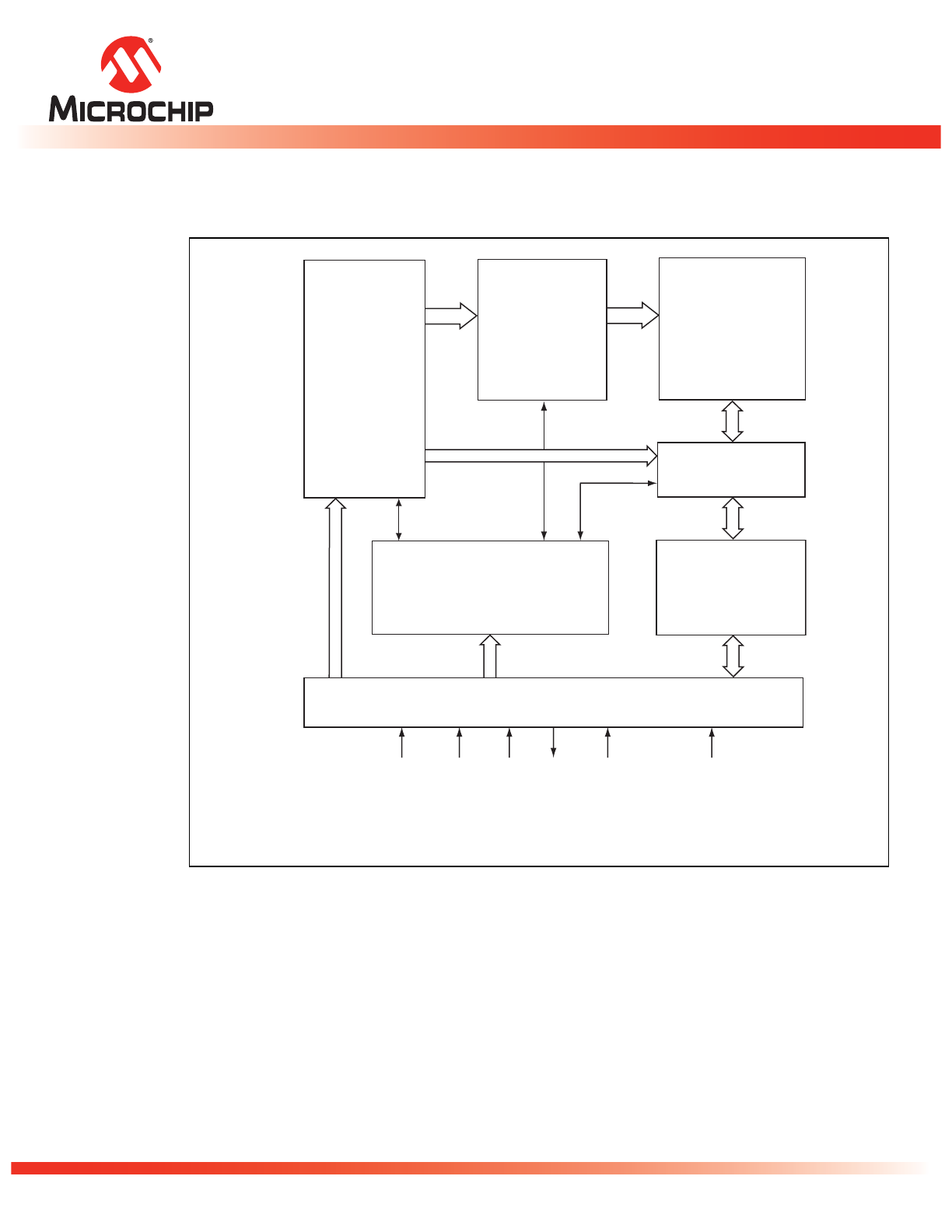
Block Diagram
Figure 1: Functional Block Diagram
1328 F01.0
I/O Buffers
and
Data Latches
SuperFlash
Memory
X - Decoder
Control Logic
Address
Buffers
and
Latches
CE#
Y - Decoder
SCK
SI
SO
WP#
RST#/HOLD#
Serial Interface
Note: In AAI mode, the SO pin functions as an RY/BY# pin when configured as a ready/
busy status pin. See “End-of-Write Detection” on page 16. for more information.
©2014 Silicon Storage Technology, Inc.
DS20005016C
11/14
4
512 Kbit / 1 Mbit / 2 Mbit / 4 Mbit 1.8V SPI Serial Flash
SST25WF512 / SST25WF010 / SST25WF020 / SST25WF040
EOL Data Sheet
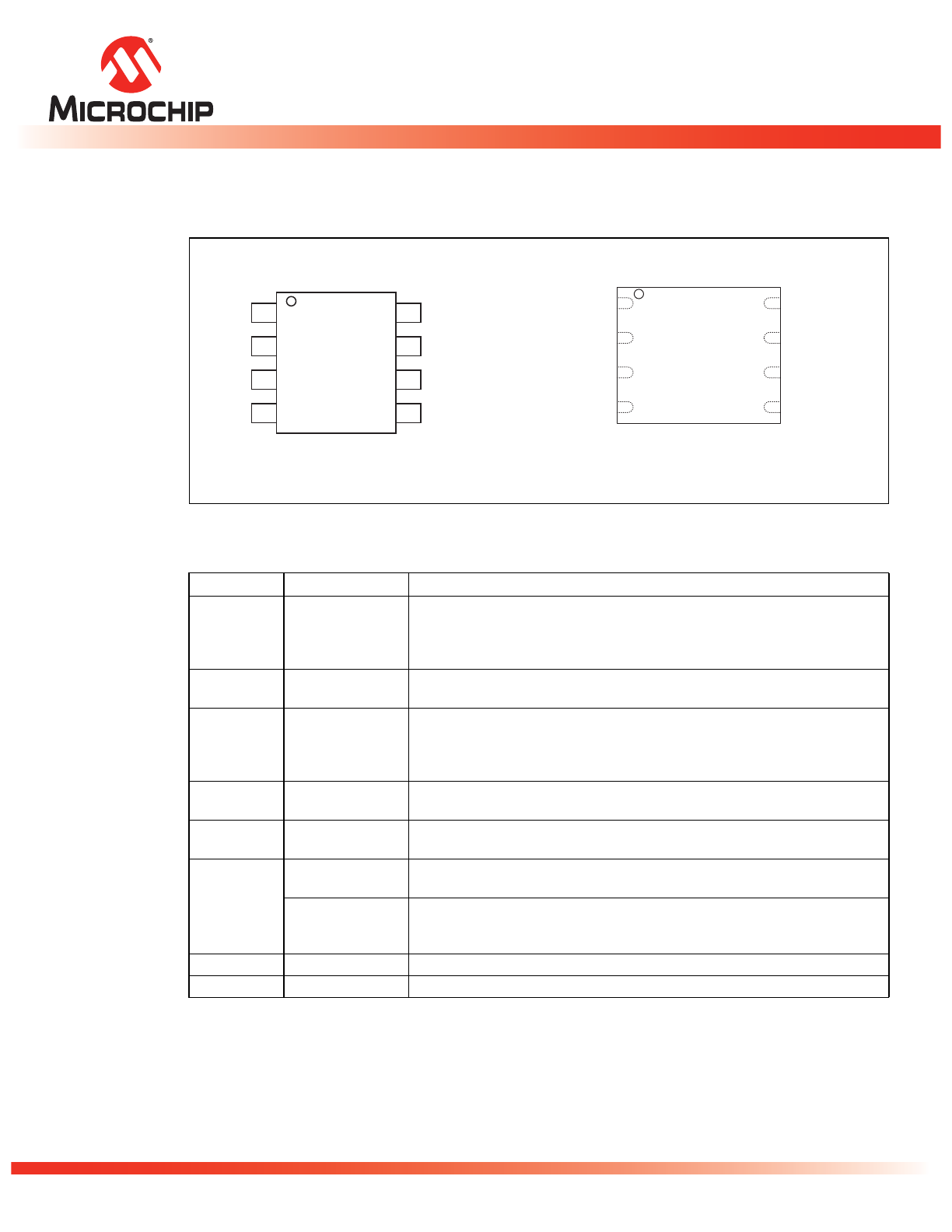
Pin Description
Figure 2: Pin Assignment for 8-Lead SOIC and 8-Contact WSON
Table 1: Pin Description
Symbol
Pin Name
Functions
SCK
Serial Clock
To provide the timing of the serial interface.
Commands, addresses, or input data are latched on the rising edge of the
clock input, while output data is shifted out on the falling edge of the clock
input.
SI
Serial Data Input
To transfer commands, addresses, or data serially into the device.
Inputs are latched on the rising edge of the serial clock.
SO
Serial Data Output To transfer data serially out of the device.
Data is shifted out on the falling edge of the serial clock.
Flash busy status pin in AAI mode if SO is configured as a hardware RY/BY#
pin. See “End-of-Write Detection” on page 16. for more information.
CE#
Chip Enable
The device is enabled by a high to low transition on CE#. CE# must remain
low for the duration of any command sequence.
WP#
Write Protect
The Write Protect (WP#) pin is used to enable/disable BPL bit in the status
register.
RST#/
HOLD#
Reset
To reset the operation of the device and the internal logic. The device powers
on with RST# pin functionality as default.
Hold
To temporarily stop serial communication with SPI Flash memory while
device is selected. This is selected by an instruction sequence which is
detailed in “Reset/Hold Mode” on page 6.
V
DD
Power Supply
To provide power supply voltage: 1.65-1.95V for SST25WF512/010/020/040
V
SS
Ground
T1.0 20005016
1
2
3
4
8
7
6
5
CE#
SO
WP#
V
SS
V
DD
RST#/HOLD#
SCK
SI
Top View
1328.25WF 08-soic-P0.0
1
2
3
4
8
7
6
5
CE#
SO
WP#
VSS
Top View
VDD
RST#/HOLD#
SCK
SI
1328 08-wson P2.0
8-Lead SOIC
8-Contact WSON
©2014 Silicon Storage Technology, Inc.
DS20005016C
11/14
5
512 Kbit / 1 Mbit / 2 Mbit / 4 Mbit 1.8V SPI Serial Flash
SST25WF512 / SST25WF010 / SST25WF020 / SST25WF040
EOL Data Sheet
Memory Organization
The SST25WF512/010/020/040 SuperFlash memory arrays are organized in uniform 4 KByte with 16
KByte, 32 KByte, and 64 KByte (2 Mbit and 4 Mbit Only) overlay erasable blocks.
Device Operation
The SST25WF512/010/020/040 are accessed through the SPI (Serial Peripheral Interface) bus com-
patible protocol. The SPI bus consist of four control lines; Chip Enable (CE#) is used to select the
device, and data is accessed through the Serial Data Input (SI), Serial Data Output (SO), and Serial
Clock (SCK).
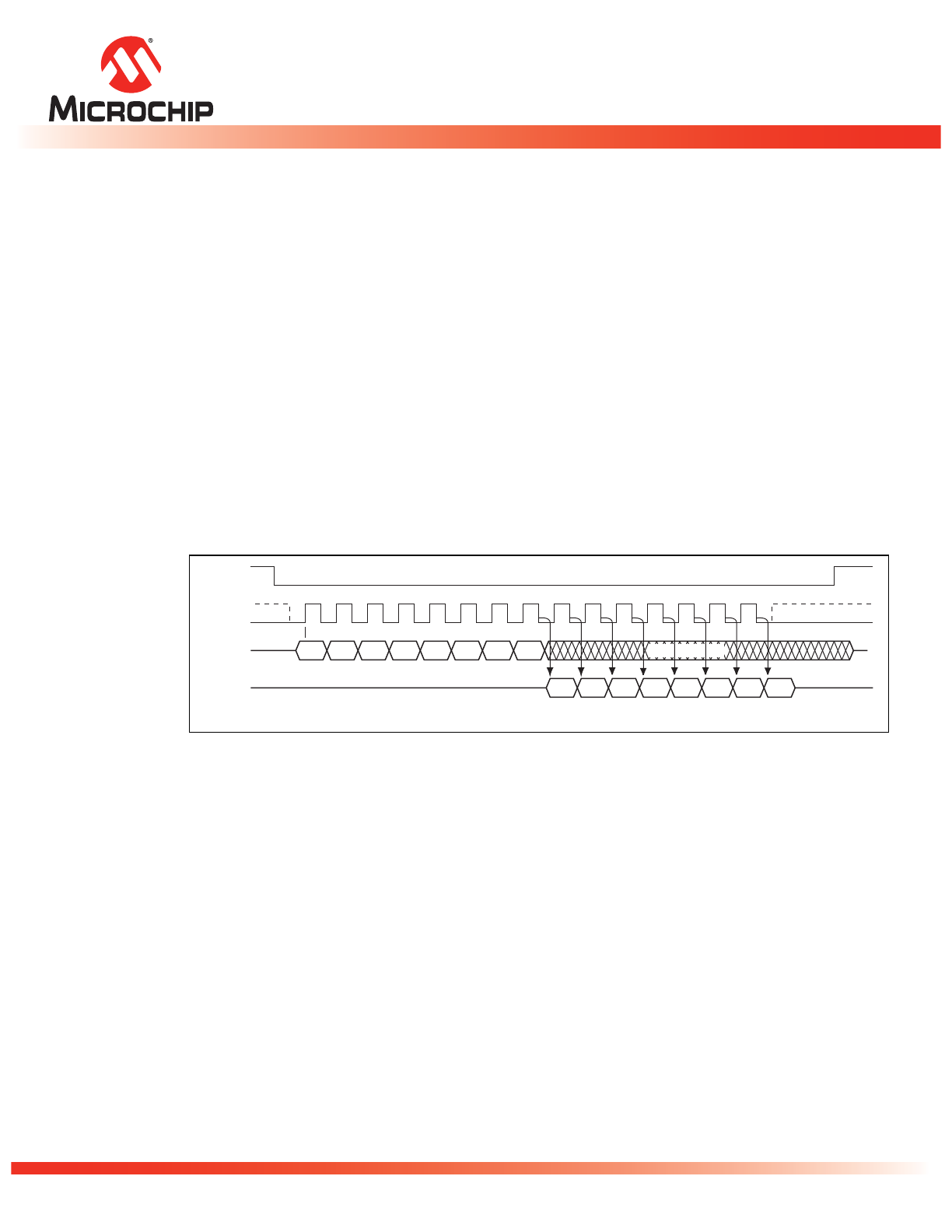
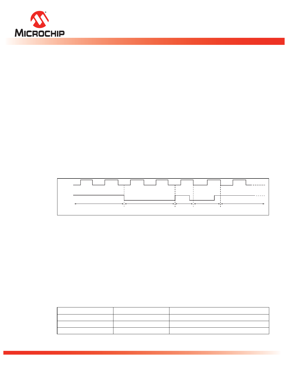
The SST25WF512/010/020/040 support both Mode 0 (0,0) and Mode 3 (1,1) of SPI bus operations.
The difference between the two modes, as shown in Figure 3, is the state of the SCK signal when the
bus master is in Stand-by mode and no data is being transferred. The SCK signal is low for Mode 0
and SCK signal is high for Mode 3. For both modes, the Serial Data In (SI) is sampled at the rising
edge of the SCK clock signal and the Serial Data Output (SO) is driven after the falling edge of the
SCK clock signal.
Figure 3: SPI Protocol
1328 F03.0
MODE 3
SCK
SI
SO
CE#
MODE 3
DON T CARE
Bit 7 Bit 6 Bit 5 Bit 4 Bit 3 Bit 2 Bit 1 Bit 0
Bit 7 Bit 6 Bit 5 Bit 4 Bit 3 Bit 2 Bit 1 Bit 0
MODE 0
MODE 0
HIGH IMPEDANCE
MSB
MSB
©2014 Silicon Storage Technology, Inc.
DS20005016C
11/14
6
512 Kbit / 1 Mbit / 2 Mbit / 4 Mbit 1.8V SPI Serial Flash
SST25WF512 / SST25WF010 / SST25WF020 / SST25WF040
EOL Data Sheet
Reset/Hold Mode
The RST#/HOLD# pin provides either a hardware reset or a hold pin. From power-on, the RST#/
HOLD# pin defaults as a hardware reset pin (RST#). The Hold mode for this pin is a user selected
option where an Enable-Hold instruction enables the Hold mode. Once selected as a hold pin
(HOLD#), the RST#/HOLD# pin will be configured as a HOLD# pin, and goes back to RST# pin only
after a power-off and power-on sequence.
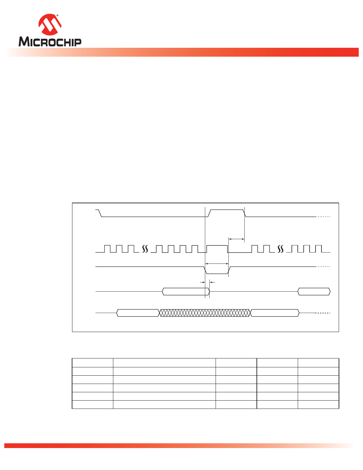
Reset
If the RST#/HOLD# pin is used as a reset pin, RST# pin provides a hardware method for resetting the
device. Driving the RST# pin high puts the device in normal operating mode. The RST# pin must be
driven low for a minimum of T
RST
time to reset the device. The SO pin is in high impedance state while
the device is in reset. A successful reset will reset the status register to its power-up state. See Table 4
for default power-up modes. A device reset during an active Program or Erase operation aborts the
operation and data of the targeted address range may be corrupted or lost due to the aborted erase or
program operation. The device exits AAI Programming Mode in progress and places the SO pin in high
impedance state.
Figure 4: Reset Timing Diagram
Table 2: Reset Timing Parameters
Symbol
Parameter
Min
Max
Units
T
RST
Reset Pulse Width
100
ns
T
RHZ
Reset to High-Z Output
107
ns
T
RECR
Reset Recovery from Read
100
ns
T
RECP
Reset Recovery from Program
10
µs
T
RECE
Reset Recovery from Erase
1
ms
T2.20005016
1328 Fx4.0
CE#
SO
SI
SCK
RST#
T
RECR
T
RECP
T
RECE
T
RST
T
RHZ
©2014 Silicon Storage Technology, Inc.
DS20005016C
11/14
7
512 Kbit / 1 Mbit / 2 Mbit / 4 Mbit 1.8V SPI Serial Flash
SST25WF512 / SST25WF010 / SST25WF020 / SST25WF040
EOL Data Sheet
Hold
The Hold operation enables the hold pin functionality of the RST#/HOLD# pin. Once set to hold pin
mode, the RST#/HOLD# pin continues functioning as a hold pin until the device is powered off and
then powered on. After a power-off and power-on, the pin functionality returns to a reset pin (RST#)
mode. See “Enable-Hold (EHLD)” on page 22 for detailed timing of the Hold instruction.
In the hold mode, serial sequences underway with the SPI Flash memory are paused without resetting
the clocking sequence. To activate the HOLD# mode, CE# must be in active low state. The HOLD#
mode begins when the SCK active low state coincides with the falling edge of the HOLD# signal. The
Hold mode ends when the rising edge of the HOLD# signal coincides with the SCK active low state. If
the falling edge of the HOLD# signal does not coincide with the SCK active low state, then the device
enters Hold mode when the SCK next reaches the active low state. Similarly, if the rising edge of the
HOLD# signal does not coincide with the SCK active low state, then the device exits Hold mode when
the SCK next reaches the active low state. See Figure 5 for Hold Condition waveform.
Once the device enters Hold mode, SO will be in high-impedance state while SI and SCK can be V
IL
or V
IH.
If CE# is driven active high during a Hold condition, the device returns to standby mode. The device
can then be re-initiated with the command sequences listed in Tables 9 and 10. As long as HOLD# sig-
nal is low, the memory remains in the Hold condition. To resume communication with the device,
HOLD# must be driven active high, and CE# must be driven active low. See Figure 5 for Hold timing.
Figure 5: Hold Condition Waveform
Write Protection
SST25WF512/010/020/040 provide software Write protection. The Write Protect pin (WP#) enables or
disables the lock-down function of the status register. The Block-Protection bits (BP2, BP1, BP0, and
BPL) in the status register provide Write protection to the memory array and the status register. See
Table 5 for the Block-Protection description.
Write Protect Pin (WP#)
The Write Protect (WP#) pin enables the lock-down function of the BPL bit (bit 7) in the status register.
When WP# is driven low, the execution of the Write-Status-Register (WRSR) instruction is determined by
the value of the BPL bit (see Table 3). When WP# is high, the lock-down function of the BPL bit is disabled.
Table 3: Conditions to execute Write-Status-Register (WRSR) Instruction
WP#
BPL
Execute WRSR Instruction
L
1
Not Allowed
L
0
Allowed
H
X
Allowed
T3.0 20005016
Active
Hold
Active
Hold
Active
1328 Fx5.0
SCK
HOLD#
©2014 Silicon Storage Technology, Inc.
DS20005016C
11/14
8
512 Kbit / 1 Mbit / 2 Mbit / 4 Mbit 1.8V SPI Serial Flash
SST25WF512 / SST25WF010 / SST25WF020 / SST25WF040
EOL Data Sheet
Status Register
The software status register provides status on whether the flash memory array is available for any
Read or Write operation, whether the device is Write enabled, and the state of the Memory Write pro-
tection. During an internal Erase or Program operation, the status register may be read only to deter-
mine the completion of an operation in progress. Table 4 describes the function of each bit in the
software status register.
Busy
The Busy bit determines whether there is an internal Erase or Program operation in progress. A ‘1’ for
the Busy bit indicates the device is busy with an operation in progress. A ‘0’ indicates the device is
ready for the next valid operation.
Write Enable Latch (WEL)
The Write-Enable-Latch bit indicates the status of the internal Write-Enable-Latch memory. If the WEL
bit is set to ‘1’, it indicates the device is Write enabled. If the bit is set to ‘0’ (reset), it indicates the
device is not Write enabled and does not accept any Write (Program/Erase) commands. The Write-
Enable-Latch bit is automatically reset under the following conditions:
•
Device Reset
•
Power-up
•
Write-Disable (WRDI) instruction completion
•
Byte-Program instruction completion
•
Auto Address Increment (AAI) programming is completed or reached its highest unpro-
tected memory address
•
Sector-Erase instruction completion
•
Block-Erase instruction completion
•
Chip-Erase instruction completion
•
Write-Status-Register instructions
Table 4: Software Status Register
Bit
Name
Function
Default at
Power-up
Read/Write
0
BUSY
1 = Internal Write operation is in progress
0 = No internal Write operation is in progress
0
R
1
WEL
1 = Device is memory Write enabled
0 = Device is not memory Write enabled
0
R
2
BP0
Indicate current level of block write protection (See Tables 5 through 8)
1
R/W
3
BP1
Indicate current level of block write protection (See Tables 5 through 8)
1
R/W
4
BP2
Indicate current level of block write protection (See Tables 5 through 8)
1
R/W
5
RES
Reserved for future use
0
N/A
6
AAI
Auto Address Increment Programming status
1 = AAI programming mode
0 = Byte-Program mode
0
R
7
BPL
1 = BP1 and BP0 are read-only bits
0 = BP1 and BP0 are read/writable
0
R/W
T4.1 20005016
©2014 Silicon Storage Technology, Inc.
DS20005016C
11/14
9
512 Kbit / 1 Mbit / 2 Mbit / 4 Mbit 1.8V SPI Serial Flash
SST25WF512 / SST25WF010 / SST25WF020 / SST25WF040
EOL Data Sheet
Auto Address Increment (AAI)
The Auto Address Increment Programming-Status bit provides status on whether the device is in AAI
programming mode or Byte-Program mode. The default at power up is Byte-Program mode.
Block-Protection (BP2, BP1, BP0)
The Block-Protection (BP1, BP0) bits define the size of the memory area to be software protected
against any memory Write (Program or Erase) operation, see Tables 5-7. The Write-Status-Register
(WRSR) instruction is used to program the BP1 and BP0 bits as long as WP# is high or the Block-Pro-
tect-Lock (BPL) bit is ‘0’. Chip-Erase can only be executed if Block-Protection bits are all ‘0’. After
power-up, BP2, BP1, and BP0 are set to defaults. See Table 4 for defaults at power-up.
Block Protection Lock-Down (BPL)
When the WP# pin is driven low (V
IL
), it enables the Block-Protection-Lock-Down (BPL) bit. When BPL is
set to ‘1’, it prevents any further alteration of the BPL, BP1, and BP0 bits. When the WP# pin is driven high
(V
IH
), the BPL bit has no effect and its value is ‘Don’t Care’. After power-up, the BPL bit is reset to ‘0’.
Table 5: Software Status Register Block Protection for SST25WF512
Protection Level
Status Register Bit
Protected Memory Address
BP1
1
1. Default at power-up for BP1 and BP0 is ‘11’.
BP0
512 Kbit
None
0
0
None
1 (Upper Quarter Memory)
0
1
00C000H-00FFFFH
2 (Upper Half Memory)
1
0
008000H-00FFFFH
3 (Full Memory)
1
1
000000H-00FFFFH
T5.1 20005016
Table 6: Software Status Register Block Protection for SST25WF010
Protection Level
Status Register Bit
Protected Memory Address
BP1
1
1. Default at power-up for BP1 and BP0 is ‘11’.
BP0
1 Mbit
None
0
0
None
1 (Upper Quarter Memory)
0
1
018000H-01FFFFH
2 (Upper Half Memory)
1
0
010000H-01FFFFH
3 (Full Memory)
1
1
000000H-01FFFFH
T6.0 20005016
Table 7: Software Status Register Block Protection for SST25WF020
Protection Level
Status Register Bit
Protected Memory Address
BP1
1
1. Default at power-up for BP1 and BP0 is ‘11’.
BP0
2 Mbit
None
0
0
None
1 (Upper Quarter Memory)
0
1
030000H-03FFFFH
2 (Upper Half Memory)
1
0
020000H-03FFFFH
3 (Full Memory)
1
1
000000H-03FFFFH
T7.0 20005016
©2014 Silicon Storage Technology, Inc.
DS20005016C
11/14
10
512 Kbit / 1 Mbit / 2 Mbit / 4 Mbit 1.8V SPI Serial Flash
SST25WF512 / SST25WF010 / SST25WF020 / SST25WF040
EOL Data Sheet
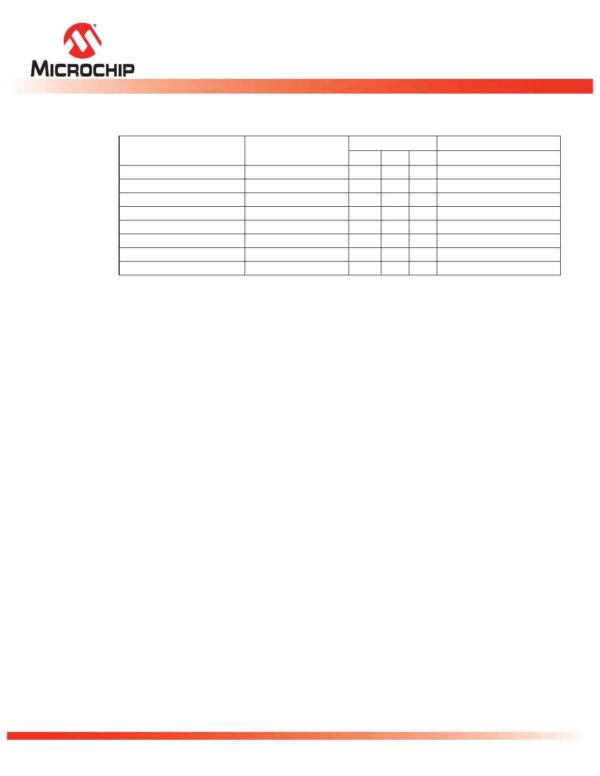
Table 8: Software Status Register Block Protection for SST25WF040
Protection Level
Protected Blocks
Status Register Bit
Protected Memory Address
BP2
1
1. Default at power-up for BP2, BP1, and BP0 is ‘11’.
BP1
BP0
4 Mbit
None
None
0
0
0
None
1 (Upper Eighth Memory)
Blocks 14 through 15
0
0
1
70000H-7FFFFH
2 (Upper Quarter Memory)
Blocks 12 through 15
0
1
0
60000H-7FFFFH
3 (Upper Half Memory)
Blocks 8 through 15
0
1
1
40000H-7FFFFH
4 (Full Memory)
Blocks 0 through 15
1
0
0
00000H-7FFFFH
5 (Full Memory)
Blocks 0 through 15
1
0
1
00000H-7FFFFH
6 (Full Memory)
Blocks 0 through 15
1
1
0
00000H-7FFFFH
7 (Full Memory)
Blocks 0 through 15
1
1
1
00000H-7FFFFH
T8.0 20005016