

2014 Microchip Technology Inc.
DS20005013D-page 1
Features
• Single Voltage Read and Write Operations
- 1.65-1.95V
• Serial Interface Architecture
- Mode 0 and Mode 3
- Nibble-wide multiplexed I/O’s with SPI-like serial
command structure
- x1/x2/x4 Serial Peripheral Interface (SPI) Proto-
col
• High Speed Clock Frequency
- 104 MHz max
• Burst Modes
- Continuous linear burst
- 8/16/32/64 Byte linear burst with wrap-around
• Superior Reliability
- Endurance: 100,000 Cycles (min)
- Greater than 100 years Data Retention
• Low Power Consumption:
- Active Read current: 15 mA (typical @ 104 MHz)
- Standby current: 10 μA (typical)
- Deep Power-Down current: 2.5 μA (typical)
• Fast Erase Time
- Sector/Block Erase: 18 ms (typ), 25 ms (max)
- Chip Erase: 35 ms (typ), 50 ms (max)
• Page-Program
- 256 Bytes per page in x1 or x4 mode
• End-of-Write Detection
- Software polling the BUSY bit in status register
• Flexible Erase Capability
- Uniform 4 KByte sectors
- Four 8 KByte top and bottom parameter overlay
blocks
- One 32 KByte top and bottom overlay block
- Uniform 64 KByte overlay blocks
• Write-Suspend
- Suspend Program or Erase operation to access
another block/sector
• Software Reset (RST) mode
• Software Protection
- Individual-Block Write Protection with permanent
lock-down capability
- 64 KByte blocks, two 32 KByte blocks, and
eight 8 KByte parameter blocks
- Read Protection on top and bottom 8 KByte
parameter blocks
• Security ID
- One-Time Programmable (OTP) 2 KByte,
Secure ID
- 64 bit unique, factory pre-programmed identifier
- User-programmable area
• Temperature Range
- Industrial: -40°C to +85°C
• Packages Available
- 8-contact WDFN (6mm x 5mm)
- 8-lead SOIC (150 mil)
- 8-ball Chip Scale Package (Z-Scale™)
• All devices are RoHS compliant
Product Description
The Serial Quad I/O™ (SQI™) family of flash-memory
devices features a six-wire, 4-bit I/O interface that
allows for low-power, high-performance operation in a
low pin-count package. SST26WF016B/016BA also
support full command-set compatibility to traditional
Serial Peripheral Interface (SPI) protocol. System
designs using SQI flash devices occupy less board
space and ultimately lower system costs.
All members of the 26 Series, SQI family are manufac-
tured with SST proprietary, high-performance CMOS
SuperFlash® technology. The split-gate cell design
and thick-oxide tunneling injector attain better reliability
and manufacturability compared with alternate
approaches.
The SST26WF016B/SST26WF016BA significantly
improves performance and reliability, while lowering
power consumption. This device writes (Program or
Erase) with a single power supply of 1.65-1.95V. The
total energy consumed is a function of the applied volt-
age, current, and time of application. Since for any
given voltage range, the SuperFlash technology uses
less current to program and has a shorter erase time,
the total energy consumed during any Erase or Pro-
gram operation is less than alternative flash memory
technologies.
SST26WF016B/016BA is offered in 8-contact WDFN
(6 mm x 5 mm), 8-lead SOIC (150 mil), and 8-ball
XFBGA (Z-Scale™) packages. See
Figure 2-1
for pin
assignments.
Two configurations are available upon order:
SST26WF016B default at power-up has the WP# and
Hold# pins enabled and SST26WF016BA default at
power-up has the WP# and Hold# pins disabled.
SST26WF016B/
SST26WF016BA
1.8V 16 Mbit Serial Quad I/O (SQI) Flash Memory

SST26WF016B/SST26WF016BA
DS20005013D-page 2
2014 Microchip Technology Inc.
TO OUR VALUED CUSTOMERS
It is our intention to provide our valued customers with the best documentation possible to ensure successful use of your Microchip
products. To this end, we will continue to improve our publications to better suit your needs. Our publications will be refined and
enhanced as new volumes and updates are introduced.
If you have any questions or comments regarding this publication, please contact the Marketing Communications Department via E-
mail at
docerrors@microchip.com
. We welcome your feedback.
Most Current Data Sheet
To obtain the most up-to-date version of this data sheet, please register at our Worldwide Web site at:
http://www.microchip.com
You can determine the version of a data sheet by examining its literature number found on the bottom outside corner of any page. The
last character of the literature number is the version number, (e.g., DS30000000A is version A of document DS30000000).
Errata
An errata sheet, describing minor operational differences from the data sheet and recommended workarounds, may exist for current
devices. As device/documentation issues become known to us, we will publish an errata sheet. The errata will specify the revision of
silicon and revision of document to which it applies.
To determine if an errata sheet exists for a particular device, please check with one of the following:
• Microchip’s Worldwide Web site;
http://www.microchip.com
• Your local Microchip sales office (see last page)
When contacting a sales office, please specify which device, revision of silicon and data sheet (include literature number) you are
using.
Customer Notification System
Register on our web site at
www.microchip.com
to receive the most current information on all of our products.
2014 Microchip Technology Inc.
DS20005013D-page 3
SST26WF016B/SST26WF016BA
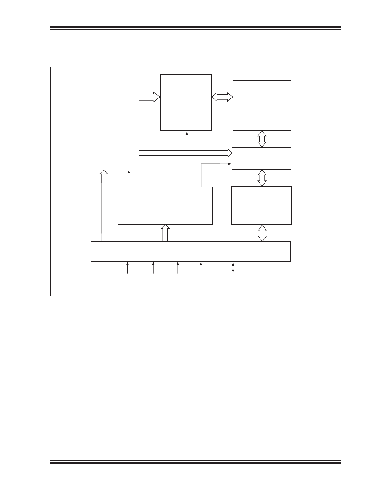
1.0
BLOCK DIAGRAM
FIGURE 1-1:
FUNCTIONAL BLOCK DIAGRAM
1432 B1.0
Page Buffer,
I/O Buffers
and
Data Latches
SuperFlash
Memory
X - Decoder
Control Logic
Address
Buffers
and
Latches
HOLD#
Y - Decoder
CE#
SIO [3:0]
Serial Interface
OTP
WP#
SCK
SST26WF016B/SST26WF016BA
DS20005013D-page 4
2014 Microchip Technology Inc.
2.0
PIN DESCRIPTION
FIGURE 2-1:
PIN DESCRIPTION FOR 8-LEAD SOIC, 8-CONTACT WDFN, AND 8-BALL XFBGA
1
2
3
4
8
7
6
5
CE#
SO/SIO1
WP#/SIO2
VSS
VDD
HOLD/SIO3
SCK
SI/SIO0
Top View
1432 08-soic S2A P1.0
1
2
3
4
8
7
6
5
CE#
SO/SIO1
WP#/SIO2
VSS
Top View
VDD
HOLD/SIO3
SCK
SI/SIO0
1432 08-wson QA P1.0
8-Lead SOIC
8-Contact WDFN
8-Ball XFBGA
Top View
8-xfbga P1.0
CE#
V
DD
SO/SIO1
HOLD/
SIO3
WP#/
SIO2
SCK
V
SS
SI/SIO0
A
B
C
D
2
1
(Balls Facing Down)
2014 Microchip Technology Inc.
DS20005013D-page 5
SST26WF016B/SST26WF016BA
TABLE 2-1:
PIN DESCRIPTION
Symbol
Pin Name
Functions
SCK
Serial Clock
To provide the timing of the serial interface.
Commands, addresses, or input data are latched on the rising edge of the clock
input, while output data is shifted out on the falling edge of the clock input.
SIO[3:0]
Serial Data
Input/Output
To transfer commands, addresses, or data serially into the device or data out of
the device. Inputs are latched on the rising edge of the serial clock. Data is
shifted out on the falling edge of the serial clock. The Enable Quad I/O (EQIO)
command instruction configures these pins for Quad I/O mode.
SI
Serial Data Input
for SPI mode
To transfer commands, addresses or data serially into the device. Inputs are
latched on the rising edge of the serial clock. SI is the default state after a
power on reset.
SO
Serial Data Output
for SPI mode
To transfer data serially out of the device. Data is shifted out on the falling edge
of the serial clock. SO is the default state after a power on reset.
CE#
Chip Enable
The device is enabled by a high to low transition on CE#. CE# must remain low
for the duration of any command sequence; or in the case of Write operations,
for the command/data input sequence.
WP#
Write Protect
The WP# pin is used in conjunction with the WPEN and IOC bits in the configu-
ration register to prohibit Write operations to the Block-Protection register. This
pin only works in SPI, single-bit and dual-bit Read mode.
HOLD#
Hold
Temporarily stops serial communication with the SPI Flash memory while the
device is selected. This pin only works in SPI, single-bit and dual-bit Read
mode. This pin must be tied high when not in use.
V
DD
Power Supply
To provide power supply voltage.
V
SS
Ground
SST26WF016B/SST26WF016BA
DS20005013D-page 6
2014 Microchip Technology Inc.
3.0
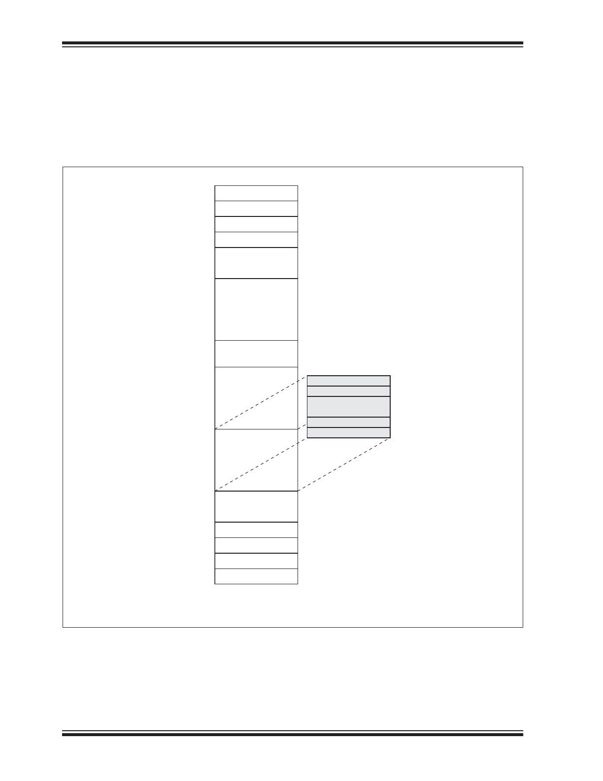
MEMORY ORGANIZATION
The SST26WF016B/016BA SQI memory array is orga-
nized in uniform, 4 KByte erasable sectors with the fol-
lowing erasable blocks: eight 8 KByte parameter, two
32 KByte overlay, and thirty 64 KByte overlay blocks.
See
Figure 3-1
.
FIGURE 3-1:
MEMORY MAP
1432 F41.0
Top of Memory Block
8 KByte
8 KByte
8 KByte
8 KByte
32 KByte
64 KByte
64 KByte
64 KByte
32 KByte
8 KByte
8 KByte
8 KByte
8 KByte
Bottom of Memory Block
4 KByte
4 KByte
4 KByte
4 KByte
. . .
2 Sectors for 8 KByte blocks
8 Sectors for 32 KByte blocks
16 Sectors for 64 KByte blocks
. . .
2014 Microchip Technology Inc.
DS20005013D-page 7
SST26WF016B/SST26WF016BA
4.0
DEVICE OPERATION
The SST26WF016B/016BA support both Serial
Peripheral Interface (SPI) bus protocol and a 4-bit mul-
tiplexed SQI bus protocol. To provide backward com-
patibility to traditional SPI Serial Flash devices, the
device’s initial state after a power-on reset is SPI mode
which supports multi-I/O (x1/x2/x4) Read/Write com-
mands. A command instruction configures the device
to SQI mode. The dataflow in the SQI mode is similar
to the SPI mode, except it uses four multiplexed I/O sig-
nals for command, address, and data sequence.
SQI Flash Memory supports both Mode 0 (0,0) and
Mode 3 (1,1) bus operations. The difference between
the two modes is the state of the SCK signal when the
bus master is in stand-by mode and no data is being
transferred. The SCK signal is low for Mode 0 and SCK
signal is high for Mode 3. For both modes, the Serial
Data I/O (SIO[3:0]) is sampled at the rising edge of the
SCK clock signal for input, and driven after the falling
edge of the SCK clock signal for output. The traditional
SPI protocol uses separate input (SI) and output (SO)
data signals as shown in
Figure 4-1
. The SQI protocol
uses four multiplexed signals, SIO[3:0], for both data in
and data out, as shown in
Figure 4-2
. This means the
SQI protocol quadruples the traditional bus transfer
speed at the same clock frequency, without the need
for more pins on the package.
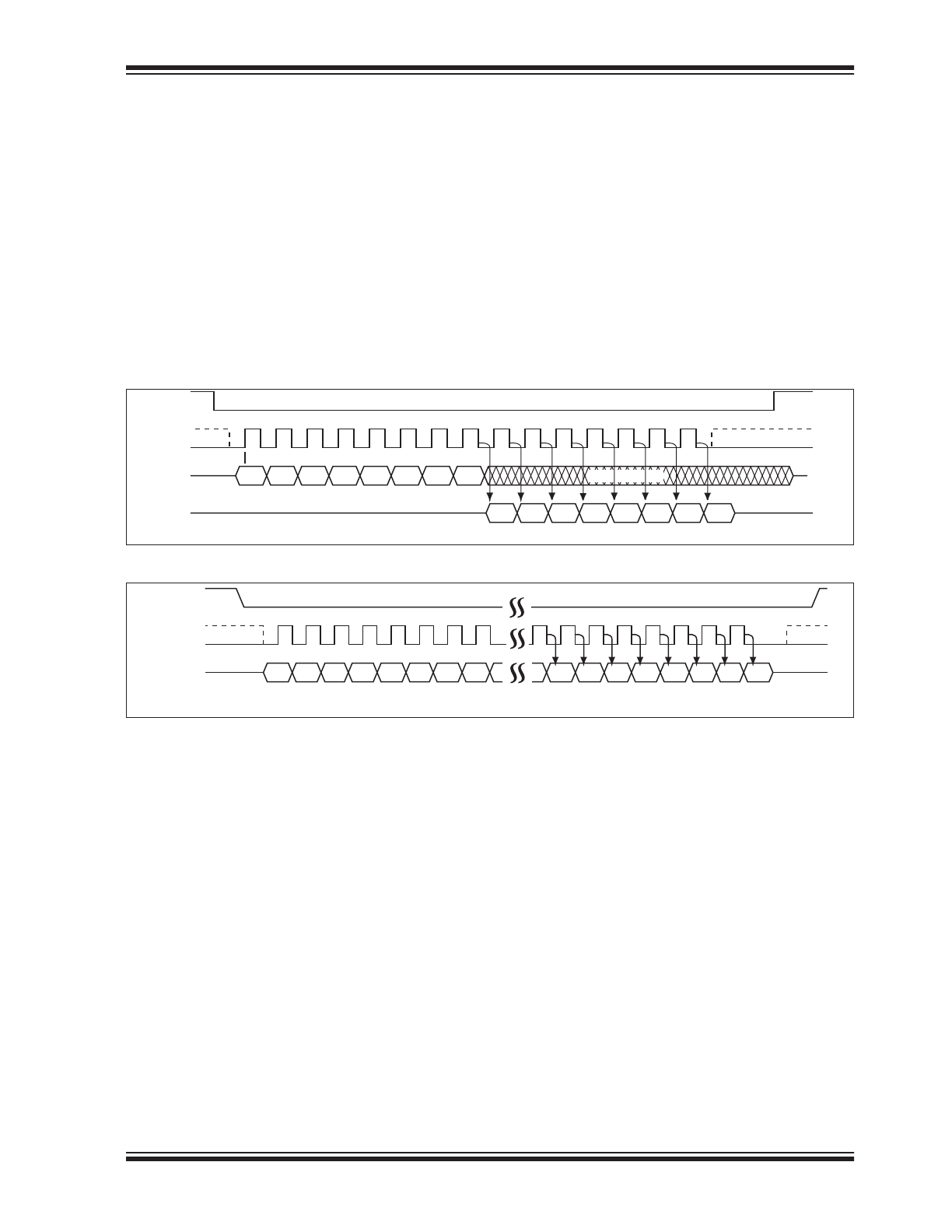
FIGURE 4-1:
SPI PROTOCOL (TRADITIONAL 25 SERIES SPI DEVICE)
FIGURE 4-2:
SQI SERIAL QUAD I/O PROTOCOL
4.1
Device Protection
The SST26WF016B/016BA offers a flexible memory
protection scheme that allows the protection state of
each individual block to be controlled separately. In addi-
tion, the Write-Protection Lock-Down register prevents
any change of the lock status during device operation.
To avoid inadvertent writes during power-up, the device
is write-protected by default after a power-on reset cycle.
A Global Block-Protection Unlock command offers a sin-
gle command cycle that unlocks the entire memory array
for faster manufacturing throughput.
For extra protection, there is an additional non-volatile
register that can permanently write-protect the Block-
Protection register bits for each individual block. Each
of the corresponding lock-down bits are one time pro-
grammable (OTP)—once written, they cannot be
erased. Data that had been previously programmed
into these blocks cannot be altered by programming or
erase and is not reversible
4.1.1
INDIVIDUAL BLOCK PROTECTION
The SST26WF016B/016BA has a Block-Protection
register which provides a software mechanism to write-
lock the individual memory blocks and write-lock, and/
or read-lock, the individual parameter blocks. The
Block-Protection register is 48 bits wide: two bits each
for the eight 8 KByte parameter blocks (write-lock and
read-lock), and one bit each for the remaining 32 KByte
and 64 KByte overlay blocks (write-lock). See
Table 5-
6
for address range protected per register bit.
Each bit in the Block-Protection register (BPR) can be
written to a ‘1’ (protected) or ‘0’ (unprotected). For the
parameter blocks, the most significant bit is for read-lock,
and the least significant bit is for write-lock. Read-locking
the parameter blocks provides additional security for sen-
sitive data after retrieval (e.g., after initial boot). If a block
is read-locked all reads to the block return data 00H.
The Write Block-Protection Register command is a
two-cycle command which requires that Write-Enable
(WREN) is executed prior to the Write Block-Protection
1432 F03.0
MODE 3
SCK
SI
SO
CE#
MODE 3
DON T CARE
Bit 7 Bit 6 Bit 5 Bit 4 Bit 3 Bit 2 Bit 1 Bit 0
Bit 7 Bit 6 Bit 5 Bit 4 Bit 3 Bit 2 Bit 1 Bit 0
MODE 0
MODE 0
HIGH IMPEDANCE
MSB
MSB
1432 F04.0
MODE 3
CLK
SIO(3:0)
CE#
MODE 3
C1
C0
A5
A4
A3
A2
A1
A0
H0
L0
H1
L1
H2
L2
H3
L3
MODE 0
MODE 0
MSB
SST26WF016B/SST26WF016BA
DS20005013D-page 8
2014 Microchip Technology Inc.
Register command. The Global Block-Protection
Unlock command clears all write protection bits in the
Block-Protection register.
4.1.2
WRITE-PROTECTION LOCK-
DOWN (VOLATILE)
To prevent changes to the Block-Protection register,
use the Lock-Down Block-Protection Register (LBPR)
command to enable Write-Protection Lock-Down.
Once Write-Protection Lock-Down is enabled, the
Block-Protection register can not be changed. To avoid
inadvertent lock down, the WREN command must be
executed prior to the LBPR command.
To reset Write-Protection Lock-Down, performing a
power cycle on the device is required. The Write-Protec-
tion Lock-Down status may be read from the Status reg-
ister.
4.1.3
WRITE-LOCK LOCK-DOWN (NON-
VOLATILE)
The non-Volatile Write-Lock Lock-Down register is an
alternate register that permanently prevents changes
to the block-protect bits. The non-Volatile Write-Lock
Lock-Down register (nVWLDR) is 40 bits wide per
device: one bit each for the eight 8-KByte parameter
blocks, and one bit each for the remaining 32 KByte
and 64 KByte overlay blocks. See
Table 5-6
for
address range protected per register bit.
Writing ‘1’ to any or all of the nVWLDR bits disables the
change mechanism for the corresponding Write-Lock
bit in the BPR, and permanently sets this bit to a ‘1’
(protected) state. After this change, both bits will be set
to ‘1’, regardless of the data entered in subsequent
writes to either the nVWLDR or the BPR. Subsequent
writes to the nVWLDR can only alter available locations
that have not been previously written to a ‘1’. This
method provides write-protection for the corresponding
memory-array block by protecting it from future pro-
gram or erase operations.
Writing a ‘0’ in any location in the nVWLDR has no effect
on either the nVWLDR or the corresponding Write-Lock
bit in the BPR.
Note that if the Block-Protection register had been pre-
viously locked down, see “ Write-Protection Lock-
Down (Volatile)”, the device must be power cycled
before using the nVWLDR. If the Block-Protection reg-
ister is locked down and the Write nVWLDR command
is accessed, the command will be ignored.
4.2
Hardware Write Protection
The hardware Write Protection pin (WP#) is used in con-
junction with the WPEN and IOC bits in the configuration
register to prohibit write operations to the Block-Protec-
tion and Configuration registers. The WP# pin function
only works in SPI single-bit and dual-bit read mode when
the IOC bit in the configuration register is set to ‘0’.
The WP# pin function is disabled when the WPEN bit
in the configuration register is ‘0’. This allows installa-
tion of the SST26WF016B/016BA in a system with a
grounded WP# pin while still enabling Write to the
Block-Protection register. The Lock-Down function of
the Block-Protection Register supersedes the WP# pin,
see
Table 4-1
for Write Protection Lock-Down states.
The factory default setting at power-up of the WPEN bit
is ‘0’, disabling the Write Protect function of the WP#
after power-up. WPEN is a non-volatile bit; once the bit
is set to ‘1’, the Write Protect function of the WP# pin
continues to be enabled after power-up. The WP# pin
only protects the Block-Protection Register and Config-
uration Register from changes. Therefore, if the WP#
pin is set to low before or after a Program or Erase
command, or while an internal Write is in progress, it
will have no effect on the Write command.
The IOC bit takes priority over the WPEN bit in the con-
figuration register. When the IOC bit is ‘1’, the function
of the WP# pin is disabled and the WPEN bit serves no
function. When the IOC bit is ‘0’ and WPEN is ‘1’, set-
ting the WP# pin active low prohibits Write operations
to the Block Protection Register.
TABLE 4-1:
WRITE PROTECTION LOCK-DOWN STATES
WP#
IOC
WPEN
WPLD
Execute WBPR Instruction
Configuration Register
L
0
1
1
Not Allowed
Protected
L
0
0
1
Not Allowed
Writable
L
0
1
0
Not Allowed
Protected
L
0
1
1. Default at power-up Register settings for SST26WF016B
0
2
2. Factory default setting is ‘0’. This is a non-volatile bit; default at power-up is the value set prior to power-down.
0
Allowed
Writable
H
0
X
1
Not Allowed
Writable
H
0
X
0
Allowed
Writable
X
1
X
1
Not Allowed
Writable
X
1
3
3. Default at power-up Register settings for SST26WF016BA
0
2
0
Allowed
Writable
2014 Microchip Technology Inc.
DS20005013D-page 9
SST26WF016B/SST26WF016BA
4.3
Security ID
SST26WF016B/016BA offers a 2 KByte Security ID
(Sec ID) feature. The Security ID space is divided into
two parts – one factory-programmed, 64-bit segment
and one user-programmable segment. The factory-
programmed segment is programmed during manufac-
turing with a unique number and cannot be changed.
The user-programmable segment is left unpro-
grammed for the customer to program as desired.
Use the Program Security ID (PSID) command to pro-
gram the Security ID using the address shown in
Table
5-5
. The Security ID can be locked using the Lockout
Security ID (LSID) command. This prevents any future
write operations to the Security ID.
The factory-programmed portion of the Security ID
can’t be programmed by the user; neither the factory-
programmed nor user-programmable areas can be
erased.
4.4
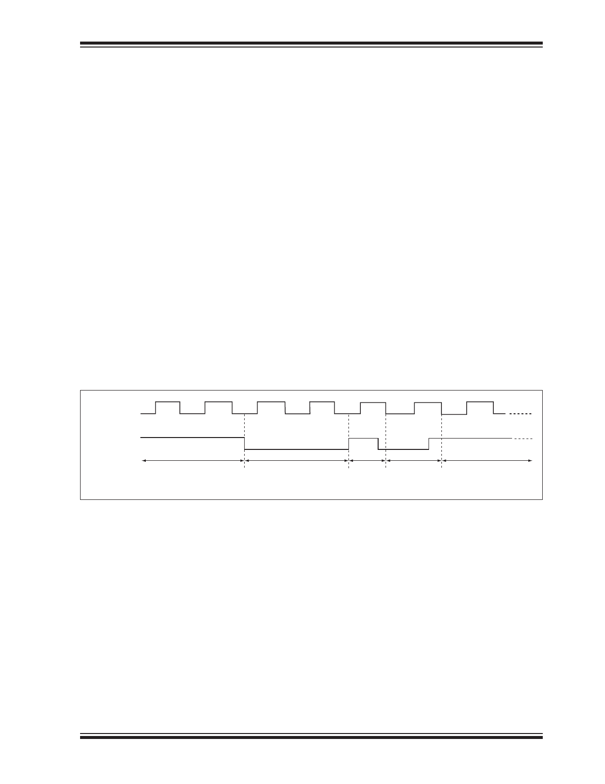
Hold Operation
The HOLD# pin pauses active serial sequences with-
out resetting the clocking sequence. This pin is active
after every power up and only operates during SPI
single-bit and dual-bit modes. Two factory configura-
tions are available: SST26WF016B ships with the IOC
bit set to ‘0’ and the HOLD# pin function enabled;
SST26WF016BA ships with the IOC bit set to ‘1’ and
the HOLD# pin function disabled. The HOLD# pin is
always disabled in SQI mode and only works in SPI sin-
gle-bit and dual-bit read mode.
To activate the Hold mode, CE# must be in active low
state. The Hold mode begins when the SCK active low
state coincides with the falling edge of the HOLD# sig-
nal. The Hold mode ends when the HOLD# signal’s ris-
ing edge coincides with the SCK active low state.
If the falling edge of the HOLD# signal does not coin-
cide with the SCK active low state, then the device
enters Hold mode when the SCK next reaches the
active low state. Similarly, if the rising edge of the
HOLD# signal does not coincide with the SCK active
low state, then the device exits Hold mode when the
SCK next reaches the active low state. See
Figure 4-3
.
Once the device enters Hold mode, SO will be in high
impedance state while SI and SCK can be V
IL
or V
IH
.
If CE# is driven active high during a Hold condition, it
resets the internal logic of the device. As long as
HOLD# signal is low, the memory remains in the Hold
condition. To resume communication with the device,
HOLD# must be driven active high, and CE# must be
driven active low.
FIGURE 4-3:
HOLD CONDITION WAVEFORM.
Active
Hold
Active
Hold
Active
1432 F46.0
SCK
HOLD#
SST26WF016B/SST26WF016BA
DS20005013D-page 10
2014 Microchip Technology Inc.
4.5
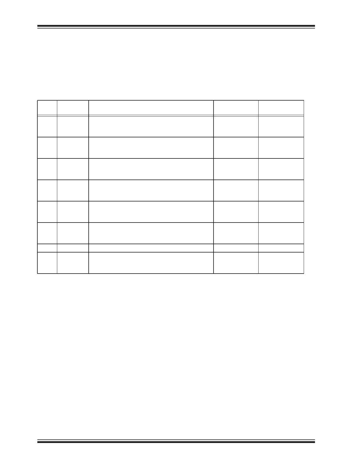
Status Register
The Status register is a read-only register that provides
the following status information: whether the flash
memory array is available for any Read or Write oper-
ation, if the device is write-enabled, whether an erase
or program operation is suspended, and if the Block-
Protection register and/or Security ID are locked down.
During an internal Erase or Program operation, the Sta-
tus register may be read to determine the completion of
an operation in progress.
Table 4-2
describes the func-
tion of each bit in the Status register.
4.5.1
WRITE-ENABLE LATCH (WEL)
The Write-Enable Latch (WEL) bit indicates the status
of the internal memory’s Write-Enable Latch. If the
WEL bit is set to ‘1’, the device is write enabled. If the
bit is set to ‘0’ (reset), the device is not write enabled
and does not accept any memory Program or Erase,
Protection Register Write, or Lock-Down commands.
The Write-Enable Latch bit is automatically reset under
the following conditions:
• Power-up
• Reset
• Write-Disable (WRDI) instruction
• Page-Program instruction completion
• Sector-Erase instruction completion
• Block-Erase instruction completion
• Chip-Erase instruction completion
• Write-Block-Protection register instruction
• Lock-Down Block-Protection register instruction
• Program Security ID instruction completion
• Lockout Security ID instruction completion
• Write-Suspend instruction
• SPI Quad Page Program
• Write Status Register
4.5.2
WRITE SUSPEND ERASE STATUS
(WSE)
The Write Suspend-Erase status (WSE) indicates
when an Erase operation has been suspended. The
WSE bit is ‘1’ after the host issues a suspend command
during an Erase operation. Once the suspended Erase
resumes, the WSE bit is reset to ‘0’.
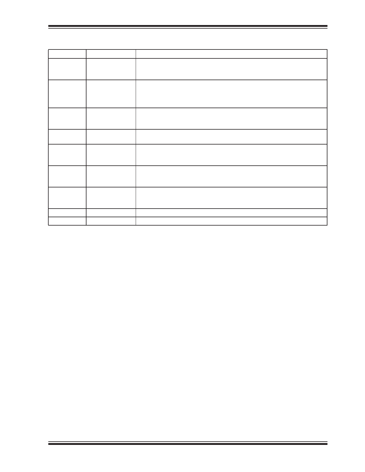
TABLE 4-2:
STATUS REGISTER
Bit
Name
Function
Default at
Power-up
Read/Write (R/
W)
0
BUSY
Write operation status
1 = Internal Write operation is in progress
0 = No internal Write operation is in progress
0
R
1
WEL
Write-Enable Latch status
1 = Device is write-enabled
0 = Device is not write-enabled
0
R
2
WSE
Write Suspend-Erase status
1 = Erase suspended
0 = Erase is not suspended
0
R
3
WSP
Write Suspend-Program status
1 = Program suspended
0 = Program is not suspended
0
R
4
WPLD
Write Protection Lock-Down status
1 = Write Protection Lock-Down enabled
0 = Write Protection Lock-Down disabled
0
R
5
SEC
1
1. The Security ID status will always be ‘1’ at power-up after a successful execution of the Lockout Security ID instruction,
otherwise default at power-up is ‘0’.
Security ID status
1 = Security ID space locked
0 = Security ID space not locked
0
1
R
6
RES
Reserved for future use
0
R
7
BUSY
Write operation status
1 = Internal Write operation is in progress
0 = No internal Write operation is in progress
0
R