

2013 Microchip Technology Inc.
Preliminary
DS20005002D-page 1
Features
• Organized as 4M x16
• Single Voltage Read and Write Operations
- 2.7-3.6V
• Superior Reliability
- Endurance: 100,000 Cycles minimum
- Greater than 100 years Data Retention
• Low Power Consumption (typical values at 5 MHz)
- Active Current: 25 mA (typical)
- Standby Current: 5 μA (typical)
- Auto Low Power Mode: 5 μA (typical)
• 128-bit Unique ID
• Security-ID Feature
- 248 Word, user One-Time-Programmable
• Protection and Security Features
- Hardware Boot Block Protection/WP# Input Pin,
Uniform (32 KWord), and Non-Uniform
(8 KWord) options available
- User-controlled individual block (32 KWord) pro-
tection, using software only methods
- Password protection
• Hardware Reset Pin (RST#)
• Fast Read and Page Read Access Times:
- 70 ns Read access time
- 25 ns Page Read access times
- 8-Word Page Read buffer
• Latched Address and Data
• Fast Erase Times:
- Block-Erase Time: 18 ms (typical)
- Chip-Erase Time: 40 ms (typical)
• Erase-Suspend/-Resume Capabilities
• Fast Word and Write-Buffer Programming Times:
- Word-Program Time: 7 μs (typical)
- Write Buffer Programming Time: 1.75 μs / Word
(typical)
- 16-Word Write Buffer
• Automatic Write Timing
- Internal V
PP
Generation
• End-of-Write Detection
- Toggle Bits
- Data# Polling
- RY/BY# Output
• CMOS I/O Compatibility
• JEDEC Standard
- Flash EEPROM Pinouts and command sets
• CFI Compliant
• Packages Available
- 48-lead TSOP
- 48-ball TFBGA
• All non-Pb (lead-free) devices are RoHS compliant
Description
The SST38VF6401B, SST38VF6402B, SST38VF6403B,
and SST38VF6404B devices are 4M x16 CMOS
Advanced Multi-Purpose Flash Plus (Advanced MPF+)
manufactured with Microchip proprietary, high-perfor-
mance CMOS SuperFlash technology. The split-gate cell
design and thick-oxide tunneling injector attain better reli-
ability and manufacturability compared with alternate
approaches. The SST38VF6401B/6402B/6403B/6404B
write (Program or Erase) with a 2.7-3.6V power supply.
These devices conform to JEDEC standard pin assign-
ments for x16 memories.
Featuring high performance Word-Program, the
SST38VF6401B/6402B/6403B/6404B provide a typical
Word-Program time of 7 μsec. For faster word-pro-
gramming performance, the Write-Buffer Programming
feature, has a typical word-program time of 1.75 μsec.
These devices use Toggle Bit, Data# Polling, or the RY/
BY# pin to indicate Program operation completion. In
addition to single-word Read, Advanced MPF+ devices
provide a Page-Read feature that enables a faster
word read time of 25 ns, eight words on the same page.
To protect against inadvertent write, the
SST38VF6401B/6402B/6403B/6404B have on-chip
hardware and Software Data Protection schemes.
Designed, manufactured, and tested for a wide spec-
trum of applications, these devices are available with
100,000 cycles minimum endurance. Data retention is
rated at greater than 100 years.
The SST38VF6401B/6402B/6403B/6404B are suited for
applications that require the convenient and economi-
cal updating of program, configuration, or data mem-
ory. For all system applications, Advanced MPF+
significantly improve performance and reliability, while
lowering power consumption. These devices inherently
use less energy during Erase and Program than alter-
native flash technologies. The total energy consumed
is a function of the applied voltage, current, and time of
application. For any given voltage range, the Super-
Flash technology uses less current to program and has
SST38VF6401B / SST38VF6402B
SST38VF6403B / SST38VF6404B
64 Mbit (x16) Advanced Multi-Purpose Flash Plus

SST38VF6401B / SST38VF6402B / SST38VF6403B / SST38VF6404B
DS20005002D-page 2
Preliminary
2013 Microchip Technology Inc.
a shorter erase time; therefore, the total energy con-
sumed during any Erase or Program operation is less
than alternative flash technologies.
These devices also improve flexibility while lowering
the cost for program, data, and configuration storage
applications. The SuperFlash technology provides
fixed Erase and Program times, independent of the
number of Erase/Program cycles that have occurred.
Therefore, the system software or hardware does not
have to be modified or de-rated as is necessary with
alternative flash technologies, whose Erase and Pro-
gram times increase with accumulated Erase/Program
cycles.
The SST38VF6401B/6402B/6403B/6404B also offer
flexible data protection features. Applications that
require memory protection from program and erase
operations can use the Boot Block, Individual Block
Protection, and Advanced Protection features. For
applications that require a permanent solution, the Irre-
versible Block Locking feature provides permanent
protection for memory blocks.
To meet high-density, surface mount requirements, the
SST38VF6401B/6402B/6403B/6404B
devices are
offered in 48-lead TSOP and 48-ball TFBGA packages.
See Figures
2-1
and for pin assignments and
Table 2-
1
for pin descriptions.
TO OUR VALUED CUSTOMERS
It is our intention to provide our valued customers with the best documentation possible to ensure successful use of your Microchip
products. To this end, we will continue to improve our publications to better suit your needs. Our publications will be refined and
enhanced as new volumes and updates are introduced.
If you have any questions or comments regarding this publication, please contact the Marketing Communications Department via
E-mail at
docerrors@microchip.com
. We welcome your feedback.
Most Current Data Sheet
To obtain the most up-to-date version of this data sheet, please register at our Worldwide Web site at:
http://www.microchip.com
You can determine the version of a data sheet by examining its literature number found on the bottom outside corner of any page.
The last character of the literature number is the version number, (e.g., DS30000000A is version A of document DS30000000).
Errata
An errata sheet, describing minor operational differences from the data sheet and recommended workarounds, may exist for current
devices. As device/documentation issues become known to us, we will publish an errata sheet. The errata will specify the revision
of silicon and revision of document to which it applies.
To determine if an errata sheet exists for a particular device, please check with one of the following:
• Microchip’s Worldwide Web site;
http://www.microchip.com
• Your local Microchip sales office (see last page)
When contacting a sales office, please specify which device, revision of silicon and data sheet (include literature number) you are
using.
Customer Notification System
Register on our web site at
www.microchip.com
to receive the most current information on all of our products.
2013 Microchip Technology Inc.
Preliminary
DS20005002D-page 3
SST38VF6401B / SST38VF6402B / SST38VF6403B / SST38VF6404B
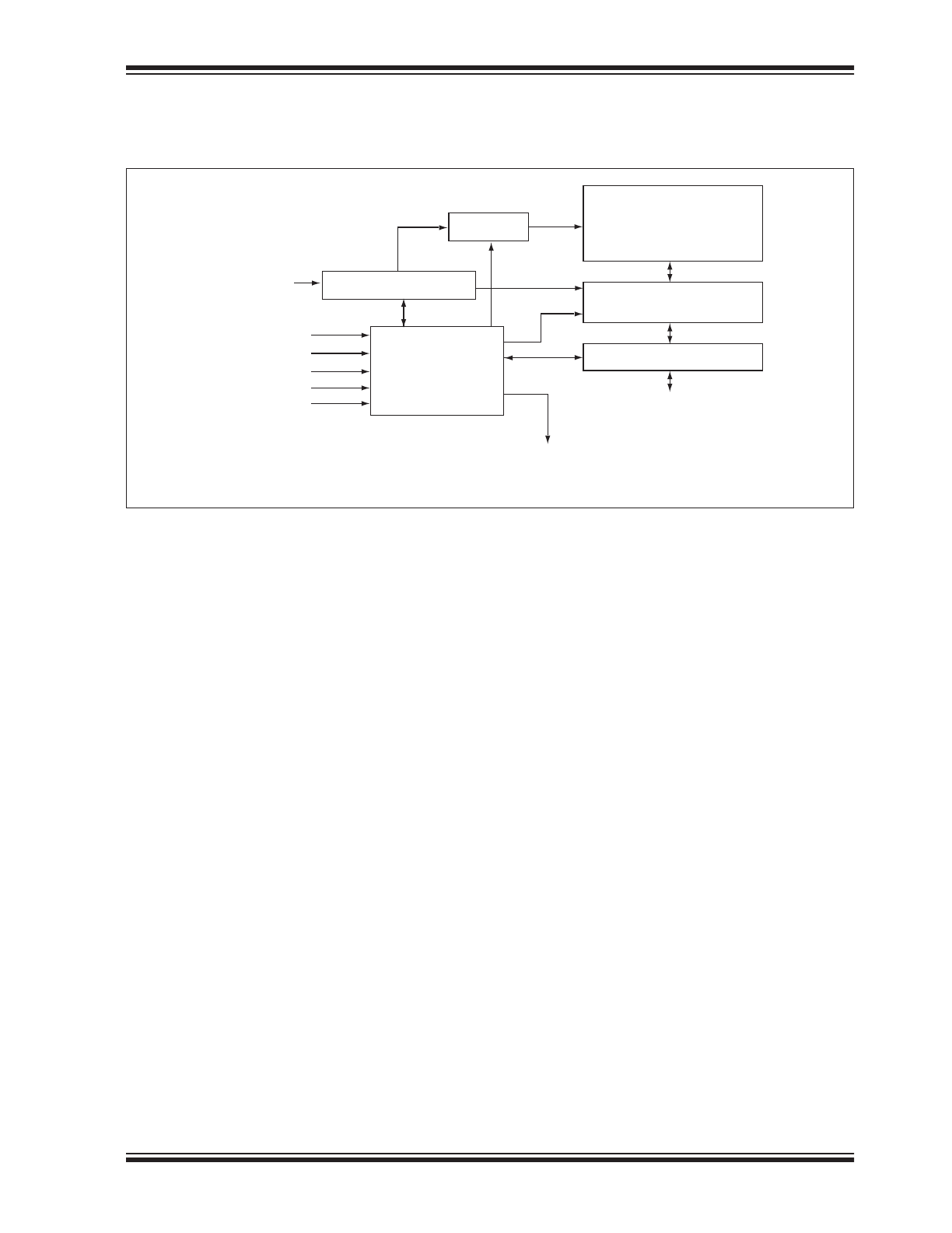
1.0
FUNCTIONAL BLOCK DIAGRAM
FIGURE 1-1:
FUNCTIONAL BLOCK DIAGRAM
Y-Decoder
I/O Buffers and Data Latches
1309 B1.1
Address Buffer Latches
X-Decoder
DQ
15
- DQ
0
Memory Address
OE#
CE#
WE#
SuperFlash
Memory
Control Logic
WP#
RST#
RY/BY#
SST38VF6401B / SST38VF6402B / SST38VF6403B / SST38VF6404B
DS20005002D-page 4
Preliminary
2013 Microchip Technology Inc.
2.0
PIN ASSIGNMENTS
FIGURE 2-1:
PIN ASSIGNMENTS FOR 48-LEAD TSOP
FIGURE 2-2:
PIN ASSIGNMENTS FOR 48-BALL TFBGA
A15
A14
A13
A12
A11
A10
A9
A8
A19
A20
WE#
RST#
A21
WP#
RY/BY#
A18
A17
A7
A6
A5
A4
A3
A2
A1
1
2
3
4
5
6
7
8
9
10
11
12
13
14
15
16
17
18
19
20
21
22
23
24
A16
NC
VSS
DQ15
DQ7
DQ14
DQ6
DQ13
DQ5
DQ12
DQ4
VDD
DQ11
DQ3
DQ10
DQ2
DQ9
DQ1
DQ8
DQ0
OE#
VSS
CE#
A0
48
47
46
45
44
43
42
41
40
39
38
37
36
35
34
33
32
31
30
29
28
27
26
25
25002 48-tsop P1.0
Standard Pinout
Top View
Die Up
25002
48-tfbga
P1.0
A B C D E F G H
6
5
4
3
2
1
TOP VIEW (balls facing down)
A13
A9
WE#
RY/BY#
A7
A3
A12
A8
RST#
WP#
A17
A4
A14
A10
A21
A18
A6
A2
A15
A11
A19
A20
A5
A1
A16
DQ7
DQ5
DQ2
DQ0
A0
NC
DQ14
DQ12
DQ10
DQ8
CE#
DQ15
DQ13
VDD
DQ11
DQ9
OE#
VSS
DQ6
DQ4
DQ3
DQ1
VSS
2013 Microchip Technology Inc.
Preliminary
DS20005002D-page 5
SST38VF6401B / SST38VF6402B / SST38VF6403B / SST38VF6404B
TABLE 2-1:
PIN DESCRIPTION
Symbol
Pin Name
Functions
A
MS
1
-A
0
Address Inputs
To provide memory addresses.
During Block-Erase A
MS
-A
15
address lines will select the block.
DQ
15
-DQ
0
Data Input/output To output data during Read cycles and receive input data during Write cycles.
Data is internally latched during a Write cycle.
The outputs are in tri-state when OE# or CE# is high.
WP#
Write Protect
To protect the top/bottom boot block from Erase/Program operation when
grounded.
RY/BY#
Ready/Busy
To indicate when the device is actively programming or erasing.
RST#
Reset
To reset and return the device to Read mode.
CE#
Chip Enable
To activate the device when CE# is low.
OE#
Output Enable
To gate the data output buffers.
WE#
Write Enable
To control the Write operations.
V
DD
Power Supply
To provide power supply voltage: 2.7-3.6V
V
SS
Ground
NC
No Connection
Unconnected pins.
1. A
MS
= Most significant address
A
MS
= A
21
for SST38VF6401B/6402B/6403B/6404B
SST38VF6401B / SST38VF6402B / SST38VF6403B / SST38VF6404B
DS20005002D-page 6
Preliminary
2013 Microchip Technology Inc.
3.0
MEMORY MAPS
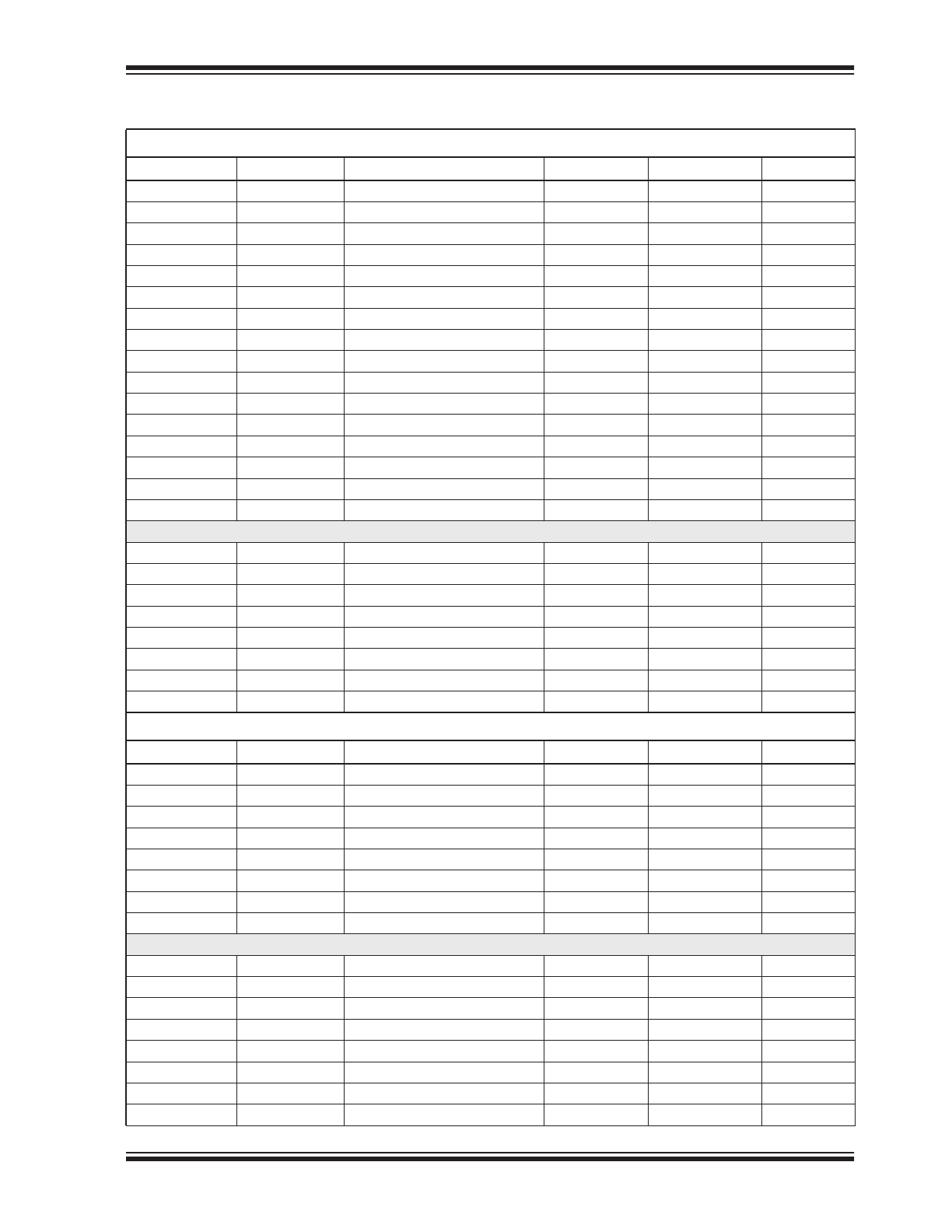
TABLE 3-1:
SST38VF6401B AND SST38VF6402B MEMORY MAPS
SST38VF6401B
Block
1
1. Each block, B0-B127 is 32KWord.
Size
Address A
21
-A
15
2
2. X = 0 or 1. Block Address (BA) = A
21
- A
15
VPB
3
3. Each block has an associated VPB and NVPB.
NVPB
3
WP#
4
4. Block B0 is the boot block.
B0
4
32 KWord
0000000
YES
YES
YES
B1
32 KWord
0000001
YES
YES
NO
B2
32 KWord
0000010
YES
YES
NO
B3
32 KWord
0000011
YES
YES
NO
B4
32 KWord
0000100
YES
YES
NO
B5
32 KWord
0000101
YES
YES
NO
B6
32 KWord
0000110
YES
YES
NO
B7
32 KWord
0000111
YES
YES
NO
B8 - B119 follow the same pattern
B120
32 KWord
1111000
YES
YES
NO
B121
32 KWord
1111001
YES
YES
NO
B122
32 KWord
1111010
YES
YES
NO
B123
32 KWord
1111011
YES
YES
NO
B124
32 KWord
1111100
YES
YES
NO
B125
32 KWord
1111101
YES
YES
NO
B126
32 KWord
1111110
YES
YES
NO
B127
32 KWord
1111111
YES
YES
NO
SST38VF6402B
Block
1
Size
Address A
21
-A
15
2
VPB
3
NVPB
3
WP#
5
5. Block B127 is the boot block.
B0
32 KWord
0000000
YES
YES
NO
B1
32 KWord
0000001
YES
YES
NO
B2
32 KWord
0000010
YES
YES
NO
B3
32 KWord
0000011
YES
YES
NO
B4
32 KWord
0000100
YES
YES
NO
B5
32 KWord
0000101
YES
YES
NO
B6
32 KWord
0000110
YES
YES
NO
B7
32 KWord
0000111
YES
YES
NO
B8 - B119 follow the same pattern
B120
32 KWord
1111000
YES
YES
NO
B121
32 KWord
1111001
YES
YES
NO
B122
32 KWord
1111010
YES
YES
NO
B123
32 KWord
1111011
YES
YES
NO
B124
32 KWord
1111100
YES
YES
NO
B125
32 KWord
1111101
YES
YES
NO
B126
32 KWord
1111110
YES
YES
NO
B127
5
32 KWord
1111111
YES
YES
YES
2013 Microchip Technology Inc.
Preliminary
DS20005002D-page 7
SST38VF6401B / SST38VF6402B / SST38VF6403B / SST38VF6404B
TABLE 3-2:
SST38VF6403B
AND SST38VF6404B MEMORY MAPS (SHEET 1 OF 2)
SST38VF6403B
Block
1
Size
Address A
21
-A
15
2
VPB
3
NVPB
3
WP#
4
B0
3,4
4 KWord
0000000000
YES
YES
YES
B1
4 KWord
0000000001
YES
YES
YES
B2
4 KWord
0000000010
YES
YES
NO
B3
4 KWord
0000000011
YES
YES
NO
B4
4 KWord
0000000100
YES
YES
NO
B5
4 KWord
0000000101
YES
YES
NO
B6
4 KWord
0000000110
YES
YES
NO
B7
4 KWord
0000000111
YES
YES
NO
B8
32 KWord
0000001XXX
YES
YES
NO
B9
32 KWord
0000010XXX
YES
YES
NO
B10
32 KWord
0000011XXX
YES
YES
NO
B11
32 KWord
0000100XXX
YES
YES
NO
B12
32 KWord
0000101XXX
YES
YES
NO
B13
32 KWord
0000110XXX
YES
YES
NO
B14
32 KWord
0000111XXX
YES
YES
NO
B15
32 KWord
0001000XXX
YES
YES
NO
B16 - B126 follow the same pattern
B127
32 KWord
1111000XXX
YES
YES
NO
B128
32 KWord
1111001XXX
YES
YES
NO
B129
32 KWord
1111010XXX
YES
YES
NO
B1230
32 KWord
1111011XXX
YES
YES
NO
B1231
32 KWord
1111100XXX
YES
YES
NO
B1232
32 KWord
1111101XXX
YES
YES
NO
B133
32 KWord
1111110XXX
YES
YES
NO
B134
32 KWord
1111111XXX
YES
YES
NO
SST38VF6404B
Block
1
Size
Address A
21
-A
15
2
VPB
3
NVPB
3
WP#
5
B0
32 KWord
0000000XXX
YES
YES
NO
B1
32 KWord
0000001XXX
YES
YES
NO
B2
32 KWord
0000010XXX
YES
YES
NO
B3
32 KWord
0000011XXX
YES
YES
NO
B4
32 KWord
0000100XXX
YES
YES
NO
B5
32 KWord
0000101XXX
YES
YES
NO
B6
32 KWord
0000110XXX
YES
YES
NO
B7
32 KWord
0000111XXX
YES
YES
NO
B8 - B119 follow the same pattern
B120
32 KWord
1111000XXX
YES
YES
NO
B121
32 KWord
1111001XXX
YES
YES
NO
B122
32 KWord
1111010XXX
YES
YES
NO
B123
32 KWord
1111011XXX
YES
YES
NO
B124
32 KWord
1111100XXX
YES
YES
NO
B125
32 KWord
1111101XXX
YES
YES
NO
B126
32 KWord
1111110XXX
YES
YES
NO
B127
3,
5
4 KWord
1111111000
YES
YES
NO

SST38VF6401B / SST38VF6402B / SST38VF6403B / SST38VF6404B
DS20005002D-page 8
Preliminary
2013 Microchip Technology Inc.
B128
4 KWord
1111111001
YES
YES
NO
B129
4 KWord
1111111010
YES
YES
NO
B130
4 KWord
1111111011
YES
YES
NO
B131
4 KWord
1111111100
YES
YES
NO
B132
4 KWord
1111111101
YES
YES
NO
B133
4 KWord
1111111110
YES
YES
YES
B134
4 KWord
1111111111
YES
YES
YES
1. Each block, B0-B127 is 32KWord.
2. X = 0 or 1. Block Address (BA) = A
21
- A
15
3. Each block has an associated VPB and NVPB, except for some blocks in SST38VF6403B and SST38VF6404B.
In SST38VF6403B, Block B0 does not have a single VPB or NVPB for all 32 KWords. Instead, each block (4 KWord) in Block
B0 has its own VPB and NVPB.
In SST38VF6404B, Block B127 does not have a single VPB or NVPB for all 32 KWords. Instead, each block (4 KWord) in
Block B127 has its own VPB and NVPB.
4. The 8KWord boot block consists of S0 and S1 in Block B0.
5. The 8KWord boot block consists of S1022 and S1023 in Block B127.
TABLE 3-2:
SST38VF6403B
AND SST38VF6404B MEMORY MAPS (CONTINUED) (SHEET 2 OF 2)

2013 Microchip Technology Inc.
Preliminary
DS20005002D-page 9
SST38VF6401B / SST38VF6402B / SST38VF6403B / SST38VF6404B
4.0
DEVICE OPERATION
The memory operations functions of these devices are
initiated using commands written to the device using
standard microprocessor Write sequences. A com-
mand is written by asserting WE# low while keeping
CE# low. The address bus is latched on the falling edge
of WE# or CE#, whichever occurs last. The data bus is
latched on the rising edge of WE# or CE#, whichever
occurs first.
The SST38VF6401B/6402B/6403B/6404B also have the
Auto Low Power mode which puts the device in a near-
standby mode after data has been accessed with a
valid Read operation. This reduces the I
DD
active read
current from typically 6 mA to typically 5 μA. The device
requires no access time to exit the Auto Low Power
mode after any address transition or control signal tran-
sition used to initiate another Read cycle. The device
does not enter Auto-Low Power mode after power-up
with CE# held steadily low, until the first address tran-
sition or CE# is driven high.
4.1
Read
The Read operation of the SST38VF6401B/6402B/
6403B/6404B is controlled by CE# and OE#, both of
which have to be low for the system to obtain data from
the outputs. CE# is used for device selection. When
CE# is high, the chip is deselected and only standby
power is consumed. OE# is the output control and is
used to gate data from the output pins. The data bus is
in high impedance state when either CE# or OE# is
high. Refer to
Figure 6-1
, the Read cycle timing dia-
gram, for further details.
4.2
Page Read
The Page Read operation utilizes an asynchronous
method that enables the system to read data from the
SST38VF6401B/6402B/6403B/6404B at a faster rate.
This operation allows users to read an eight-word page
of data at an average speed of 33 ns per word.
In Page Read, the initial word read from the page
requires T
ACC
to be valid, while the remaining seven
words in the page require only T
PACC
. All eight words in
the page have the same address bits, A
21
-A
3
, which
are used to select the page. Address bits A
2
-A
0
are tog-
gled, in any order, to read the words within the page.
The Page Read operation of the SST38VF6401B/
6402B/6403B/6404B is controlled by CE# and OE#.
Both CE# and OE# must be low for the system to obtain
data from the output pins. CE# controls device selec-
tion. When CE# is high, the chip is deselected and only
standby power is consumed. OE# is the output control
and is used to gate data from the output pins. The data
bus is in high impedance state when either CE# or OE#
is high. Refer to
Figure 6-3
, the Page Read cycle timing
diagram, for further details.
4.3
Word-Program Operation
The SST38VF6401B/6402B/6403B/6404B can be pro-
grammed on a word-by-word basis. Before program-
ming, the block where the word exists must be fully
erased. The Program operation is accomplished in
three steps. The first step is the three-byte load
sequence for Software Data Protection. The second
step is to load word address and word data. During the
Word-Program operation, the addresses are latched
on the falling edge of either CE# or WE#, whichever
occurs last. The data is latched on the rising edge of
either CE# or WE#, whichever occurs first. The third
step is the internal Program operation which is initiated
after the rising edge of the fourth WE# or CE#, which-
ever occurs first. The Program operation, once initi-
ated, will be completed within 7 μs. See Figures
6-3
and
6-4
for WE# and CE# controlled Program opera-
tion timing diagrams and
Figure 6-19
for flowcharts.
During the Program operation, the only valid reads are
Data# Polling, Toggle Bits, and RY/BY#. During the
internal Program operation, the host is free to perform
additional tasks. Any commands issued during the
internal Program operation are ignored. During the
command sequence, WP# should be statically held
high or low.
When programming more than a few words, Microchip
recommends Write-Buffer Programming.
4.4
Write-Buffer Programming
The SST38VF6401B/6402B/6403B/6404B offer Write-
Buffer Programming, a feature that enables faster
effective word programming. To use this feature, write
up to 16 words with the Write-to-Buffer command, then
use the Program Buffer-to-Flash command to program
the Write-Buffer to memory.
The Write-to-Buffer command consists of between 5
and 20 write cycles. The total number of write cycles in
the Write-to-Buffer command sequence is equal to the
number of words to be written to the buffer plus four.
The first three cycles in the command sequence tell the
device that a Write-to-Buffer operation will begin.
The fourth cycle tells the device the number of words to
be written into the buffer and the block address of these
words. Specifically, the write cycle consists of a block
address and a data value called the Word Count (WC),
which is the number of words to be written to the buffer
minus one. If the WC is greater than 15, the maximum
buffer size minus 1, then the operation aborts.
For the fifth cycle, and all subsequent cycles of the
Write-to-Buffer command, the command sequence
consists of the addresses and data of the words to be
written into the buffer. All of these cycles must have the
same A
21
- A
4
address, otherwise the operation aborts.
The number of Write cycles required is equal to the
number of words to be written into the Write-Buffer,
which is equal to WC plus one. The correct number of

SST38VF6401B / SST38VF6402B / SST38VF6403B / SST38VF6404B
DS20005002D-page 10
Preliminary
2013 Microchip Technology Inc.
Write cycles must be issued or the operation will abort.
Each Write cycle decrements the Write-Buffer counter,
even if two or more of the Write cycles have identical
address values. Only the final data loaded for each buf-
fer location is held in the Write-Buffer.
Once the Write-to-Buffer command sequence is com-
pleted, the Program Buffer-to-Flash command should
be issued to program the Write-Buffer contents to the
specified block in memory. The block address (i.e. A
21
- A
15
) in this command must match the block address
in the 4th write cycle of the Write-to-Buffer command or
the operation aborts. See
Table 5-2
for details on
Write-to-Buffer and Program-Buffer-to-Flash com-
mands.
While issuing these command sequences, the Write-
Buffer Programming Abort detection bit (DQ1) indi-
cates if the operation has aborted. There are several
cases in which the device can abort:
• In the fourth write cycle of the Write-to-Buffer
command, if the WC is greater than 15, the opera-
tion aborts.
• In the fifth and all subsequent cycles of the Write-
to-Buffer command, if the address values, A
21
-
A
4
, are not identical, the operation aborts.
• If the number of write cycles between the fifth to
the last cycle of the Write-to-Buffer command is
greater than WC +1, the operation aborts.
• After completing the Write-to-Buffer command
sequence, issuing any command other than the
Program Buffer-to-Flash command, aborts the
operation.
• Loading a block address, i.e. A
21
-A
15,
in the Pro-
gram Buffer-to-Flash command that does not
match the block address used in the Write-to-Buf-
fer command aborts the operation.
If the Write-to-Buffer or Program Buffer-to-Flash opera-
tion aborts, then DQ
1
= 1 and the device enters Write-
Buffer-Abort mode. To execute another operation, a
Write-to-Buffer Abort-Reset command must be issued
to clear DQ
1
and return the device to standard read
mode.
After the Write-to-Buffer and Program Buffer-to-Flash
commands are successfully issued, the programming
operation can be monitored using Data# Polling, Tog-
gle Bits, and RY/BY#.
4.5
Block-Erase Operations
The Block-Erase operation allows the system to erase
the device on a block-by-block basis.
The Block-Erase architecture is based on block size of
32 KWords. In SST38VF6401B and SST38VF6402B
devices, the Block-Erase command can erase any
32KWord Block (B0-B127). For the non-uniform boot
block devices, SST38VF6403B and SST38VF6404B,
the Block-Erase command can erase any 32 KWord
block except the block that contains the boot area. In
the boot area, Block-Erase only erases a 4KWord
block.
The Block-Erase operation is initiated by executing a
six-byte command sequence with Block-Erase com-
mand (30H) and block address (BA) in the last bus
cycle. The block address is latched on the falling edge
of the sixth WE# pulse, while the command (30H) is
latched on the rising edge of the sixth WE# pulse. The
internal Erase operation begins after the sixth WE#
pulse. The End-of-Erase operation can be determined
using either Data# Polling or Toggle Bit methods. The
RY/BY# pin can also be used to monitor the erase
operation. For more information, see Figure
6-10
for
timing waveforms and
Figure 6-24
for the flowchart.
Any commands, other than Erase-Suspend, issued
during the Block-Erase operation are ignored. Any
attempt to Block-Erase memory inside a block pro-
tected by Volatile Block Protection, Non-Volatile Block
Protection, or WP# (low) will be ignored. During the
command sequence, WP# should be statically held
high or low.
4.6
Erase-Suspend/Erase-Resume
Commands
The Erase-Suspend operation temporarily suspends a
Block-Erase operation thus allowing data to be read or
programmed into any block that is not engaged in an
Erase operation. The operation is executed with a one-
byte command sequence with Erase-Suspend com-
mand (B0H). The device automatically enters read
mode within 20 μs (max) after the Erase-Suspend com-
mand had been issued. Valid data can be read, using
a Read or Page Read operation, from any block that is
not being erased. Reading at an address location
within Erase-Suspended blocks will output DQ
2
tog-
gling and DQ
6
at ‘1’. While in Erase-Suspend, a Word-
Program or Write-Buffer Programming operation is
allowed anywhere except the block selected for Erase-
Suspend.
To resume a suspended Block-Erase operation, the
system must issue the Erase-Resume command. The
operation is executed by issuing one byte command
sequence with Erase-Resume command (30H) at any
address in the last Byte sequence.
When an erase operation is suspended, or re-sus-
pended, after resume the cumulative time needed for
the erase operation to complete is greater than the
erase time of a non-suspended erase operation. If the
hold time from Erase-Resume to the next Erase- Sus-
pend operation is less than 200μs, the accumulative
erase time can become very long Therefore, after issu-
ing an Erase-Resume command, the system must wait
at least 200μs before issuing another Erase-Suspend
command. The Erase-Resume command will be
ignored until any program operations initiated during
Erase-Suspend are complete.