
2002-2014 Microchip Technology Inc.
DS20001423J-page 1
TC4426A/TC4427A/TC4428A
Features:
• High Peak Output Current: 1.5A
• Wide Input Supply Voltage Operating Range:
- 4.5V to 18V
• High Capacitive Load Drive Capability: 1000 pF in
25 ns (typical)
• Short Delay Times: 30 ns (typical)
• Matched Rise, Fall and Delay Times
• Low Supply Current:
- With Logic ‘1’ Input – 1 mA (typical)
- With Logic ‘0’ Input – 100 µA (typical)
• Low Output Impedance: 7
(typical)
• Latch-Up Protected: Will Withstand 0.5A Reverse
Current
• Input Withstands Negative Inputs Up to 5V
• Electrostatic Discharge (ESD) Protected: 2 kV
• Pin-compatible with TC426/TC427/TC428 and
TC4426/TC4427/TC4428
• Space-saving 8-Pin MSOP and 8-Pin 6x5 DFN-S
Packages
Applications:
• Switch Mode Power Supplies
• Line Drivers
• Pulse Transformer Drive
General Description:
The TC4426A/TC4427A/TC4428A are improved
versions of the earlier TC4426/TC4427/TC4428 family
of MOSFET drivers. In addition to matched rise and fall
times, the TC4426A/TC4427A/TC4428A devices have
matched leading and falling edge propagation delay
times.
These devices are highly latch-up resistant under any
conditions within their power and voltage ratings. They
are not subject to damage when up to 5V of noise
spiking (of either polarity) occurs on the Ground pin.
They can accept, without damage or logic upset, up to
500 mA of reverse current (of either polarity) being
forced back into their outputs. All terminals are fully
protected against Electrostatic Discharge (ESD) up
to 2 kV.
The TC4426A/TC4427A/TC4428A MOSFET drivers
can easily charge/discharge 1000 pF gate
capacitances in under 30 ns. These devices provide
low enough impedances in both the On and Off states
to ensure the MOSFET’s intended state will not be
affected, even by large transients.
Package Types
8-Pin 6x5 DFN-S*
NC
IN A
GND
IN B
1
2
3
4
NC
5
6
7
8
OUT A
OUT B
NC
IN A
GND
IN B
V
DD
NC
OUT A
OUT B
V
DD
NC
OUT A
OUT B
V
DD
NC
OUT A
OUT B
V
DD
NC
OUT A
OUT B
V
DD
NC
OUT A
OUT B
V
DD
8-Pin MSOP/
PDIP/SOIC
TC4426A
TC4427A
TC4428A
TC4427A
TC4426A
TC4428A
1
2
3
4
8
7
6
5
EP
9
* Includes Exposed Thermal Pad (EP); see
Table 3-1
.
1.5A Dual High-Speed Power MOSFET Drivers
TC4426A/TC4427A/TC4428A
DS20001423J-page 2
2002-2014 Microchip Technology Inc.
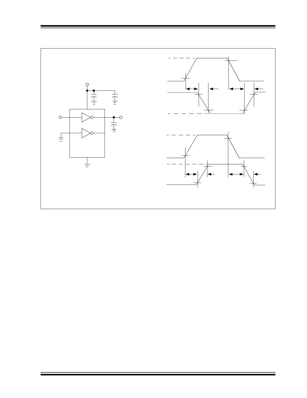
Functional Block Diagram
Effective
Input C = 12 pF
(Each Input)
TC4426A/TC4427A/TC4428A
Output
Input
GND
V
DD
300 mV
4.7V
Inverting
Non-Inverting
Note 1: TC4426A has two inverting drivers, while the TC4427A has two non-inverting
drivers. The TC4428A has one inverting and one non-inverting driver.
2: Ground any unused driver input.
500
A
2002-2014 Microchip Technology Inc.
DS20001423J-page 3
TC4426A/TC4427A/TC4428A
1.0
ELECTRICAL
CHARACTERISTICS
Absolute Maximum Ratings†
Supply Voltage ................................................................+22V
Input Voltage, IN A or IN B .......... (V
DD
+ 0.3V) to (GND – 5V)
Package Power Dissipation (T
A
+70°C)
DFN-S .....................................................................
Note 2
MSOP .....................................................................340 mW
PDIP .......................................................................730 mW
SOIC.......................................................................470 mW
† Notice: Stresses above those listed under “Absolute Maxi-
mum Ratings” may cause permanent damage to the device.
These are stress ratings only and functional operation of the
device at these or any other conditions above those indicated
in the operation sections of the specifications is not implied.
Exposure to Absolute Maximum Rating conditions for
extended periods may affect device reliability.
DC CHARACTERISTICS
Electrical Specifications: Unless otherwise noted, over operating temperature range with 4.5V
V
DD
18V.
Parameters
Sym.
Min.
Typ.
Max.
Units
Conditions
Input
Logic ‘1’, High Input
Voltage
V
IH
2.4
—
—
V
Logic ‘0’, Low Input Voltage
V
IL
—
—
0.8
V
Input Current
I
IN
–1.0
—
+1.0
µA
0V
V
IN
V
DD
–10
—
+10
Output
High Output Voltage
V
OH
V
DD
– 0.025
—
—
V
DC Test
Low Output Voltage
V
OL
—
—
0.025
V
DC Test
Output Resistance
R
O
—
7
9
I
OUT
= 10 mA, V
DD
= 18V, T
A
= +25°C
—
7
10
0°C
T
A
+70°C
—
8
11
-40°C
T
A
+85°C
—
8
12
-40°C
T
A
+125°C
Peak Output Current
I
PK
—
1.5
—
A
V
DD
= 18V
Latch-Up Protection
Withstand Reverse Current
I
REV
—
> 0.5
—
A
Duty cycle
2%, t 300 µs
V
DD
= 18V
Switching Time (
Note 1
)
Rise Time
t
R
—
25
35
ns
T
A
= +25°C
—
27
40
0°C
T
A
+70°C
—
29
40
-40°C
T
A
+85°C
—
30
40
-40°C
T
A
+125°C,
Figure 4-1
Fall Time
t
F
—
25
35
ns
T
A
= +25°C
—
27
40
0°C
T
A
+70°C
—
29
40
-40°C
T
A
+85°C
—
30
40
-40°C
T
A
+125°C,
Figure 4-1
Delay Time
t
D1
—
30
35
ns
T
A
= +25°C
—
33
40
0°C
T
A
+70°C
—
35
45
-40°C
T
A
+85°C
—
38
50
-40°C
T
A
+125°C,
Figure 4-1
Note 1:
Switching times ensured by design.
2:
Package power dissipation is dependent on the copper pad area on the PCB.
TC4426A/TC4427A/TC4428A
DS20001423J-page 4
2002-2014 Microchip Technology Inc.
Delay Time
t
D2
—
30
35
ns
T
A
= +25°C
—
33
40
0°C
T
A
+70°C
—
35
45
-40°C
T
A
+85°C
—
38
50
-40°C
T
A
+125°C,
Figure 4-1
Power Supply
Power Supply Current
I
S
—
1.0
2.0
mA
V
IN
= 3V (Both inputs)
—
0.1
0.2
V
IN
= 0V (Both inputs), V
DD
= 18V
TEMPERATURE CHARACTERISTICS
Electrical Specifications: Unless otherwise noted, all parameters apply with 4.5V
V
DD
18V.
Parameters
Sym.
Min.
Typ.
Max.
Units
Conditions
Temperature Ranges
Specified Temperature Range (C)
T
A
0
—
+70
°C
Specified Temperature Range (E)
T
A
-40
—
+85
°C
Specified Temperature Range (V)
T
A
-40
—
+125
°C
Maximum Junction Temperature
T
J
—
—
+150
°C
Storage Temperature Range
T
A
-65
—
+150
°C
Package Thermal Resistances
Thermal Resistance, 8L-6x5 DFN-S
JA
—
35.7
—
°C/W
Thermal Resistance, 8L-MSOP
JA
—
211
—
°C/W
Thermal Resistance, 8L-PDIP
JA
—
89.3
—
°C/W
Thermal Resistance, 8L-SOIC
JA
—
149.5
—
°C/W
DC CHARACTERISTICS (CONTINUED)
Electrical Specifications: Unless otherwise noted, over operating temperature range with 4.5V
V
DD
18V.
Parameters
Sym.
Min.
Typ.
Max.
Units
Conditions
Note 1:
Switching times ensured by design.
2:
Package power dissipation is dependent on the copper pad area on the PCB.
2002-2014 Microchip Technology Inc.
DS20001423J-page 5
TC4426A/TC4427A/TC4428A
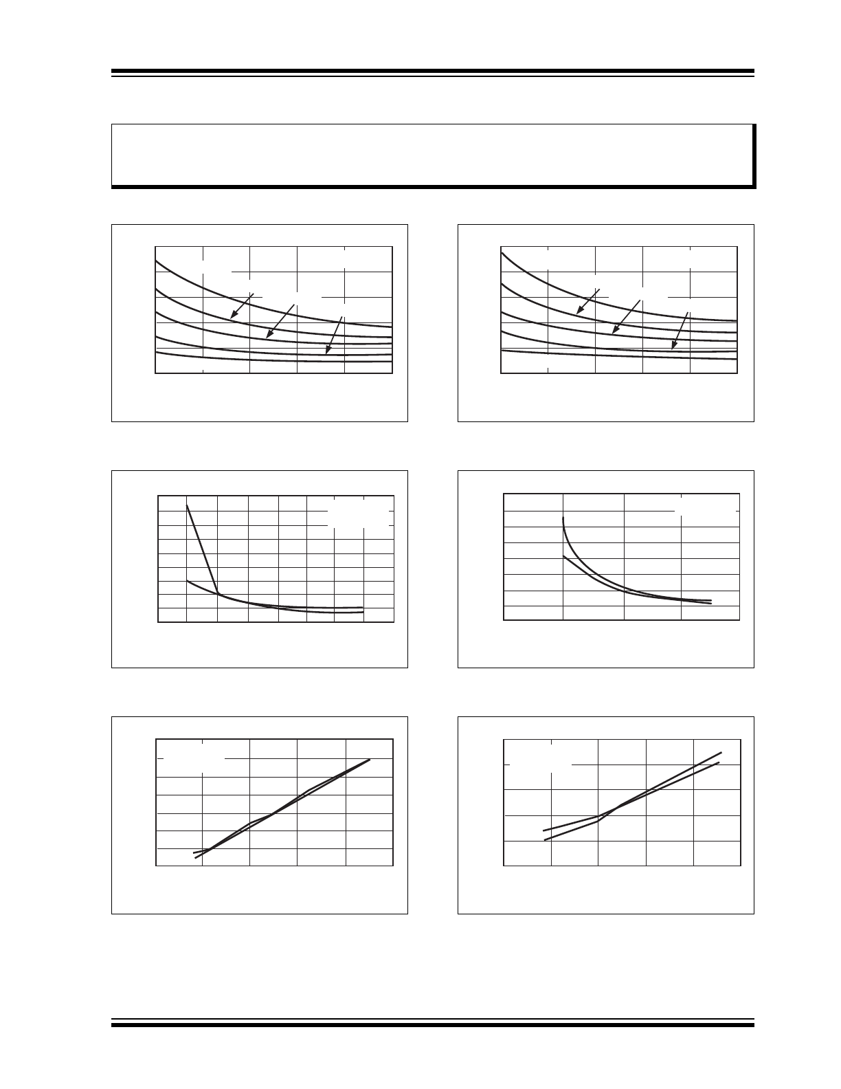
2.0
TYPICAL PERFORMANCE CURVES
Note: Unless otherwise indicated, over operating temperature range with 4.5V
V
DD
18V.
FIGURE 2-1:
Rise Time vs. Supply
Voltage.
FIGURE 2-2:
Delay Time vs. Input
Amplitude.
FIGURE 2-3:
Rise and Fall Times vs.
Temperature.
FIGURE 2-4:
Fall Time vs. Supply
Voltage.
FIGURE 2-5:
Propagation Delay Time vs.
Supply Voltage.
FIGURE 2-6:
Propagation Delay Time vs.
Temperature.
Note:
The graphs and tables provided following this note are a statistical summary based on a limited number of
samples and are provided for informational purposes only. The performance characteristics listed herein
are not tested or guaranteed. In some graphs or tables, the data presented may be outside the specified
operating range (e.g., outside specified power supply range) and therefore outside the warranted range.
5.0
7.5
10.0
12.5
15.0
17.5
0
20
40
60
80
100
T
A
= +25°C
V
DD
(V)
C
L
= 2200 pF
C
L
= 1500 pF
C
L
= 100 pF
C
L
= 1000 pF
C
L
= 470 pF
t
RISE
(nsec)
1
2
3
4
5
6
7
8
9
20
70
60
50
40
30
80
90
100
110
Delay Time (nsec)
Input Amplitude (V)
C
L
= 1000 pF
V
DD
= 10V
t
D1
t
D2
-100
-50
0
50
100
150
24
22
20
18
16
14
26
28
Time (nsec)
C
L
= 1000 pF
V
DD
= 18V
TEMPERATURE (
°C)
t
FALL
t
RISE
5.0
7.5
10.0
12.5
15.0
17.5
0
20
40
60
80
100
CL= 100pF
T
A
= +25°C
V
DD
(V)
C
L
= 2200pF
C
L
= 2200 pF
C
L
= 1500 pF
C
L
= 100 pF
C
L
= 1000 pF
C
L
= 470 pF
t
FALL
(nsec)
0
5
10
15
20
50
45
40
35
30
25
20
55
60
Delay Time (nsec)
V
DD
(V)
C
L
= 1000 pF
t
D1
t
D2
15
20
25
30
35
40
Delay Time (nsec)
-100
-50
0
50
100
150
C
L
= 1000 pF
V
DD
= 18V
TEMPERATURE (
°C)
t
D1
t
D2
TC4426A/TC4427A/TC4428A
DS20001423J-page 6
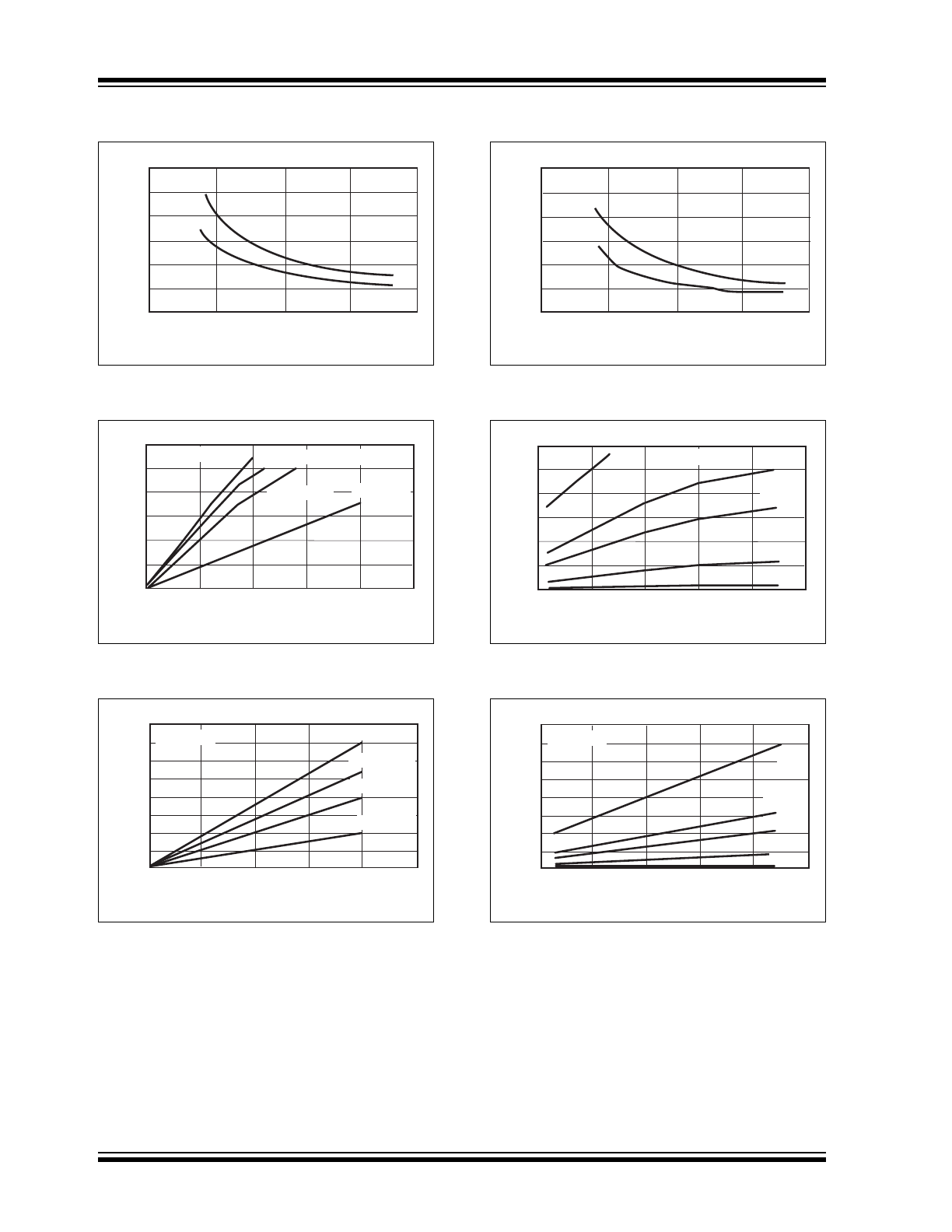
2002-2014 Microchip Technology Inc.
Note: Unless otherwise indicated, over operating temperature range with 4.5V
V
DD
18V.
FIGURE 2-7:
High-State Output
Resistance.
FIGURE 2-8:
Supply Current vs.
Frequency.
FIGURE 2-9:
Supply Current vs.
Frequency.
FIGURE 2-10:
Low-State Output
Resistance.
FIGURE 2-11:
Supply Current vs.
Capacitive Load.
FIGURE 2-12:
Supply Current vs.
Capacitive Load.
0
5
10
15
20
25
20
15
10
5
0
30
V
DD
(V)
R
DS(ON)
(
Ω
)
T
A
= +125°C
T
A
= +25°C
0
500
1000
1500
2000
2500
0
20
10
30
40
50
60
FREQUENCY (kHz)
I
SUPPLY
(mA)
V
DD
= 18V
C
L
= 2200 pF
C
L
= 1500 pF
C
L
= 1000 pF
C
L
= 100 pF
FREQUENCY (kHz)
0
500
1000
1500
2000
2500
70
60
50
40
30
20
10
0
80
I
SUPPLY
(mA)
V
DD
= 12V
C
L
= 2200 pF
C
L
= 1500 pF
C
L
= 1000 pF
C
L
= 100 pF
0
5
10
15
20
25
20
15
10
5
0
30
V
DD
(V)
R
DS(ON)
(
Ω
)
T
A
= +125°C
T
A
= +25°C
0
500
1000
1500
2000
2500
0
20
10
30
40
50
60
2 MHz
V
DD
= 18V
I
SUPPLY
(mA)
C
LOAD
(pF)
900 kHz
600 kHz
200 kHz
20 kHz
0
500
1000
1500
2000
2500
70
60
50
40
30
20
10
0
80
I
SUPPLY
(mA)
C
LOAD
(pF)
V
DD
= 12V
900 kHz
600 kHz
200 kHz
20 kHz
2 MHz
2002-2014 Microchip Technology Inc.
DS20001423J-page 7
TC4426A/TC4427A/TC4428A
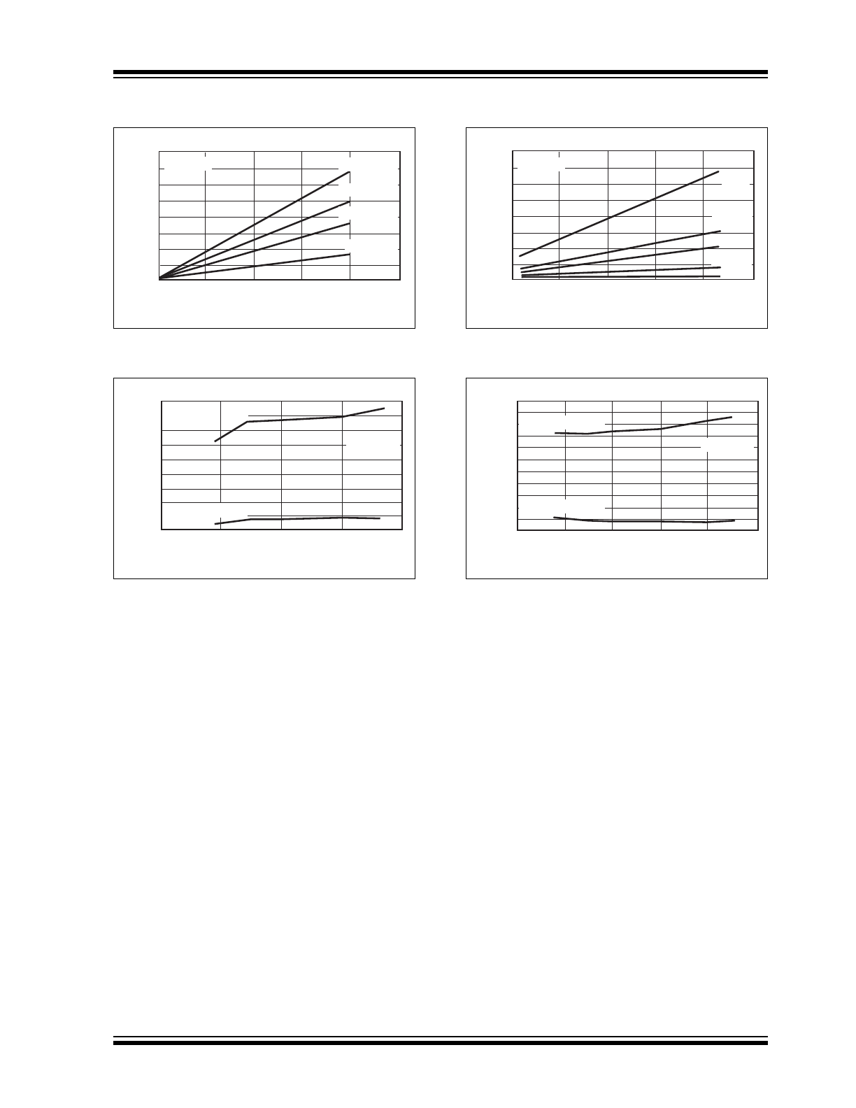
Note: Unless otherwise indicated, over operating temperature range with 4.5V
V
DD
18V.
FIGURE 2-13:
Supply Current vs.
Frequency.
FIGURE 2-14:
Quiescent Supply Current
vs. Voltage.
FIGURE 2-15:
Supply Current vs.
Capacitive Load.
FIGURE 2-16:
Quiescent Supply Current
vs. Temperature.
0
500
1000
1500
2000
2500
30
25
20
15
10
5
0
35
40
FREQUENCY (kHz)
I
SUPPLY
(mA)
V
DD
= 6V
C
L
= 2200 pF
C
L
= 1500 pF
C
L
= 1000 pF
C
L
= 100 pF
T
A
= 25°C
BOTH INPUTS = 1
0
5
10
15
20
800
700
600
500
400
200
100
0
300
900
I
QUIESCENT
(µA)
V
DD
(V)
BOTH INPUTS = 0
0
500
1000
1500
2000
2500
30
25
15
10
5
0
35
40
I
SUPPLY
(mA)
C
LOAD
(pF)
V
DD
= 6V
900 kHz
600 kHz
200 kHz
20 kHz
2 MHz
20
-100
-50
0
50
100
150
1000
900
800
700
600
400
300
200
100
0
500
1100
I
QUIESCENT
(µA)
TEMPERATURE (
°C)
V
DD
= 18V
BOTH INPUTS = 1
BOTH INPUTS = 0
TC4426A/TC4427A/TC4428A
DS20001423J-page 8
2002-2014 Microchip Technology Inc.
3.0
PIN DESCRIPTIONS
The descriptions of the pins are listed in
Table 3-1
.
3.1
Inputs A and B (IN A, IN B)
MOSFET driver inputs A and B are high-impedance,
TTL/CMOS compatible inputs. These inputs also have
300 mV of hysteresis between the high and low
thresholds that prevents output glitching, even when
the rise and fall time of the input signal is very slow.
3.2
Ground (GND)
The Ground pin is the return path for both the bias
current and the high-peak current that discharges the
external load capacitance. The Ground pin should be
tied into a ground plane or have a very short trace to the
bias supply source return.
3.3
Output A and B (OUT A, OUT B)
MOSFET driver outputs A and B are low-impedance,
CMOS push-pull style outputs. The pull-down and
pull-up devices are of equal strength, making the rise
and fall times equivalent.
3.4
Supply Input (V
DD
)
The V
DD
input is the bias supply for the MOSFET driver
and is rated for 4.5V to 18V, with respect to the ground
pin. The V
DD
input should be bypassed with local
ceramic capacitors. The value of these capacitors
should be chosen based on the capacitive load that is
being driven.
3.5
Exposed Metal Pad (EP)
The exposed metal pad of the 6x5 DFN-S package is
not internally connected to any potential. Therefore,
this pad can be connected to a ground plane or other
copper plane on a printed circuit board, to aid in heat
removal from the package.
TABLE 3-1:
PIN FUNCTION TABLE (
Note 1
)
PDIP, MSOP, SOIC
6x5 DFN-S
Symbol
Description
1
1
NC
No connection
2
2
IN A
Input A
3
3
GND
Ground
4
4
IN B
Input B
5
5
OUT B
Output B
6
6
V
DD
Supply input
7
7
OUT A
Output A
8
8
NC
No connection
—
9
EP
Exposed Metal Pad
Note 1:
Duplicate pins must be connected for proper operation.
2002-2014 Microchip Technology Inc.
DS20001423J-page 9
TC4426A/TC4427A/TC4428A
4.0
APPLICATIONS INFORMATION
FIGURE 4-1:
Switching Time Test Circuit.
C
L
= 1000 pF
0.1 µF
4.7 µF
Inverting Driver
Non-Inverting Driver
Input
V
DD
= 18V
Input
Output
t
D1
t
F
t
R
t
D2
Input: 100 kHz,
square wave,
t
RISE
= t
FALL
10 ns
Output
Input
Output
t
D1
t
F
t
R
t
D2
+5V
10%
90%
10%
90%
10%
90%
V
DD
0V
90%
10%
10%
10%
90%
+5V
V
DD
0V
0V
0V
90%
3
2
7
6
4
5
(TC4426A, ½ TC4428A)
(TC4427A, ½ TC4428A)
TC4426A/TC4427A/TC4428A
DS20001423J-page 10
2002-2014 Microchip Technology Inc.
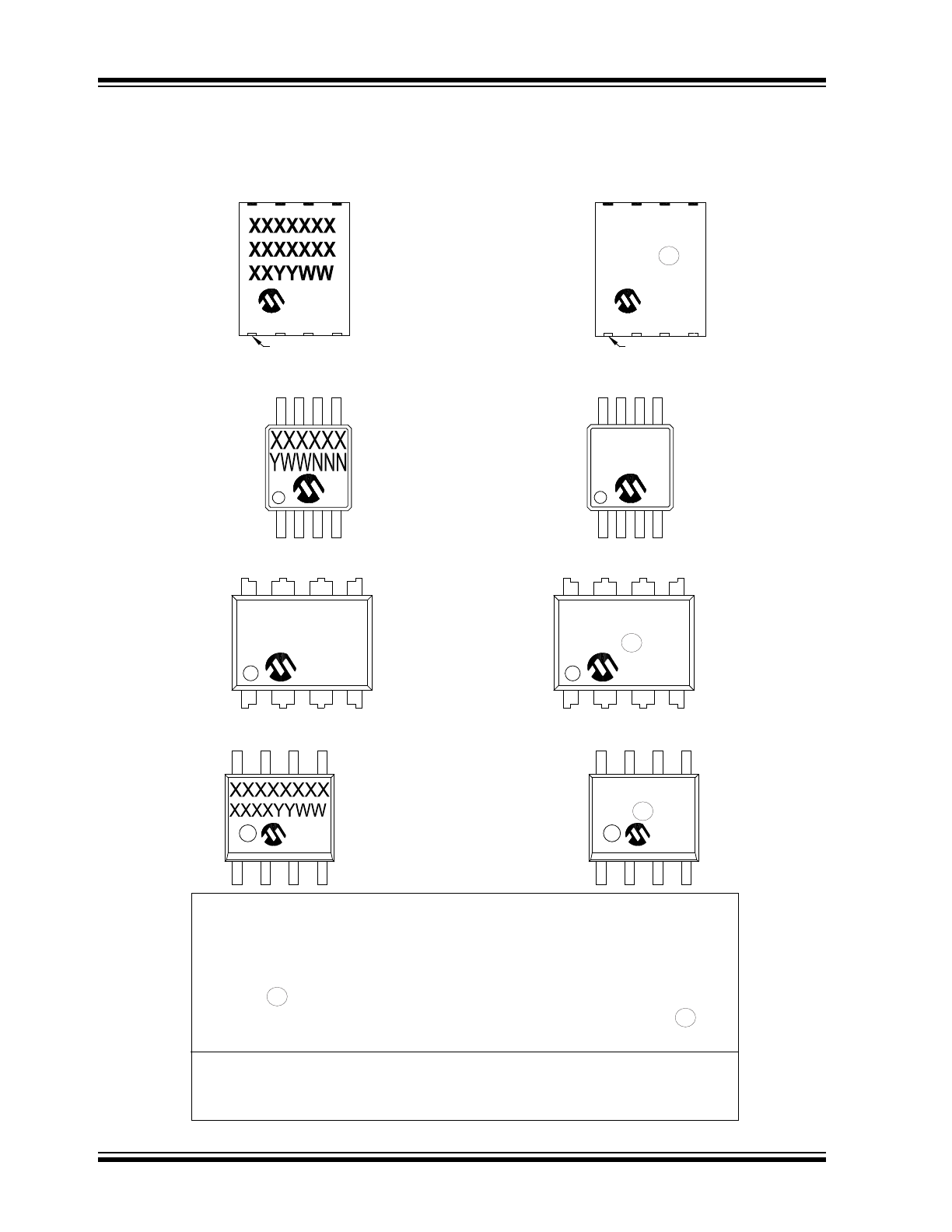
5.0
PACKAGING INFORMATION
5.1
Package Marking Information
Legend: XX...X
Customer-specific information
Y
Year code (last digit of calendar year)
YY
Year code (last 2 digits of calendar year)
WW
Week code (week of January 1 is week ‘01’)
NNN
Alphanumeric traceability code
Pb-free JEDEC
®
designator for Matte Tin (Sn)
*
This package is Pb-free. The Pb-free JEDEC designator ( )
can be found on the outer packaging for this package.
Note:
In the event the full Microchip part number cannot be marked on one line, it will
be carried over to the next line, thus limiting the number of available
characters for customer-specific information.
3
e
3
e
8-Lead DFN-S (6x5x0.9 mm)
Example
PIN 1
NNN
PIN 1
TC4426A
EMF ^^
1330
256
3
e
8-Lead MSOP (3x3 mm)
Example
4426AE
330256
8-Lead PDIP (300 mil)
Example
XXXXXXXX
XXXXXNNN
YYWW
TC4427A
EPA ^^ 256
1330
3
e
8-Lead SOIC (3.90 mm)
Example
NNN
TC2248AC
OA ^^ 330
256
3
e