
2017 Microchip Technology Inc.
DS20005718A-page 1
MIC5201
Features
• High Output Voltage Accuracy
• Variety of Output Voltages
• Guaranteed 200 mA Output
• Low Quiescent Current
• Low Dropout Voltage
• Extremely Tight Load and Line Regulation
• Very Low Temperature Coefficient
• Current and Thermal Limiting
• Reversed-Battery Protection
• Load-Dump Protection (Fixed Voltage Versions)
• Zero Off-Mode Current
• Logic-Controlled Electronic Enable
• Available in SOIC-8 and SOT-223 Packages
Applications
• Cellular Telephones
• Laptop, Notebook, and Palmtop Computers
• Battery Powered Equipment
• PCMCIA V
CC
and V
PP
Regulation/Switching
• Barcode Scanners
• SMPS Post-Regulator and DC/DC Modules
• High-Efficiency Linear Power Supplies
General Description
The MIC5201 is an efficient linear voltage regulator
with very low dropout voltage (typically 17 mV at light
loads and 200 mV at 100 mA), and very low ground
current (1 mA at 100 mA output), offering better than
1% initial accuracy with a logic compatible on-off
switching input.
Designed especially for hand-held battery powered
devices, the MIC5201 can be switched by a CMOS or
TTL compatible enable signal. This enable control may
be connected directly to V
IN
if unneeded. When
disabled, power consumption drops nearly to zero. The
ground current of the MIC5201 increases only slightly
in dropout, further prolonging battery life. Key MIC5201
features include current limiting, overtemperature
shutdown, and protection against reversed battery.
The MIC5201 is available in several fixed voltages and
accuracy configurations. It features the same pinout as
the LT1121 with better performance. Other options are
available; contact Microchip for details.
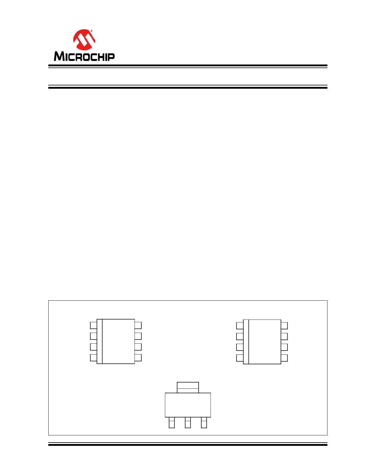
Package Types
MIC5201 (A
DJ
.)
8-Lead SOIC (M)
1
2
3
4
8
7
6
5
IN
NC
NC
EN
OUT
ADJ
GND
NC
1
2
3
4
8
7
6
5
IN
NC
NC
EN
OUT
NC
GND
NC
MIC5201 (F
IXED
)
8-Lead SOIC (M)
IN
OUT
GND
1
3
2
TAB
GND
MIC5201 (F
IXED
)
SOT-223 (S)
200 mA Low Dropout Regulator
MIC5201
DS20005718A-page 2
2017 Microchip Technology Inc.
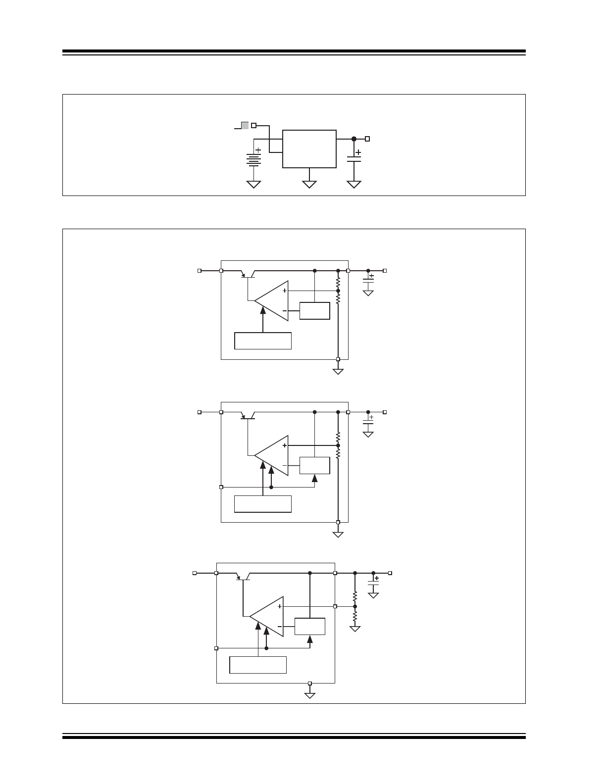
Typical Application Circuit
Functional Diagrams
ENABLE
SHUTDOWN
MIC5201-3.3
IN
OUT
GND
1μF
V
OUT
3.3V
EN
MIC5201
Current-Limit
Thermal Shutdown
IN
OUT
GND
Bandgap
Ref.
C
OUT
V
OUT
V
IN
MIC5201-x.xYS
F
IXED
R
EGULATOR
(SOT-223 V
ERSION
O
NLY
)
IN
EN
OUT
GND
V
REF
Bandgap
Ref.
Current-Limit
Thermal Shutdown
C
OUT
V
OUT
V
IN
MIC5201-x.xYM
F
IXED
R
EGULATOR
IN
EN
OUT
GND
V
REF
Bandgap
Ref.
Current-Limit
Thermal Shutdown
C
OUT
V
OUT
V
IN
R1
R2
MIC5201YM [adj.]
ADJ
A
DJUSTABLE
R
EGULATOR

2017 Microchip Technology Inc.
DS20005718A-page 3
MIC5201
1.0
ELECTRICAL CHARACTERISTICS
Absolute Maximum Ratings †
Supply Input Voltage (V
IN
) Fixed................................................................................................................. –20V to +60V
Supply Input Voltage (V
IN
) Adjustable......................................................................................................... –20V to +20V
Enable Input Voltage (V
EN
) Fixed ............................................................................................................... –20V to +60V
Enable Input Voltage (V
EN
) Adjustable ....................................................................................................... –20V to +20V
Power Dissipation (
Note 1
) .................................................................................................................... Internally Limited
Operating Ratings ‡
Supply Input Voltage (V
IN
) Fixed................................................................................................................ +2.5V to +26V
Supply Input Voltage (V
IN
) Adjustable........................................................................................................ +2.5V to +16V
Enable Input Voltage (V
EN
) .................................................................................................................................0V to V
IN
† Notice: Stresses above those listed under “Absolute Maximum Ratings” may cause permanent damage to the device.
This is a stress rating only and functional operation of the device at those or any other conditions above those indicated
in the operational sections of this specification is not intended. Exposure to maximum rating conditions for extended
periods may affect device reliability.
‡ Notice: The device is not guaranteed to function outside its operating ratings.
Note 1: The maximum allowable power dissipation is a function of the maximum junction temperature, T
J(max)
, the
junction-to-ambient thermal resistance, θ
JA
, and the ambient temperature, T
A
. The maximum allowable
power dissipation at any ambient temperature is calculated using: P
(max)
= (T
J(max)
– T
A
) ÷ θ
JA
. Exceeding
the maximum allowable power dissipation will result in excessive die temperature, and the regulator will go
into thermal shutdown.
MIC5201
DS20005718A-page 4
2017 Microchip Technology Inc.
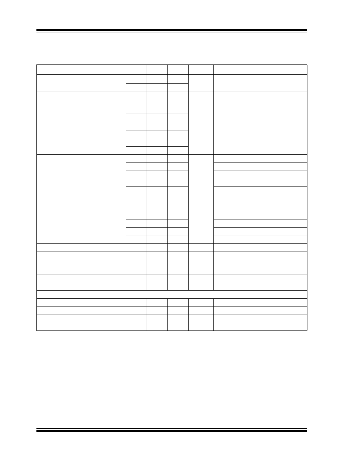
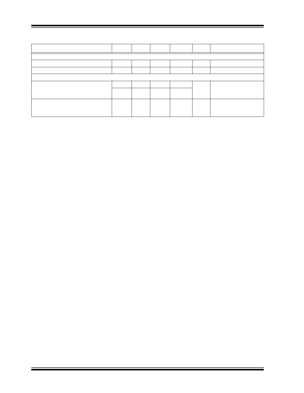
TABLE 1-1:
ELECTRICAL CHARACTERISTICS (
Note 1
)
Electrical Characteristics: V
IN
= V
OUT
+ 1V; I
L
= 100 μA; C
L
= 3.3 μF; V
EN
≥ 2.0V; T
J
= +25°C, bold values indicate
–40°C ≤ T
J
≤ +85°C; unless noted.
Parameter
Symbol
Min.
Typ.
Max.
Units
Conditions
Output Voltage Accuracy
V
O
–1
—
1
%
Variation from specified V
OUT
–2
—
2
Output Voltage
Temperature Coefficient
∆V
O
/∆T
—
40
150
ppm/°C
Note 2
Line Regulation, Fixed
∆V
O
/∆V
O
—
0.004
0.20
%
V
IN
= V
OUT
+ 1V to 26V
—
—
0.40
Line Regulation,
Adjustable
∆V
O
/∆V
O
—
0.004
0.20
%
V
IN
= V
OUT
+ 1V to 16V
—
—
0.40
Load Regulation
∆V
O
/∆V
O
—
0.04
0.16
%
I
L
= 0.1 mA to 200 mA,
Note 3
—
—
0.30
Dropout Voltage,
Note 4
V
IN
– V
O
—
17
—
mV
I
L
= 100 µA
—
130
—
I
L
= 20 mA
—
180
—
I
L
= 50 mA
—
225
—
I
L
= 100 mA
—
270
400
I
L
= 200 mA
Quiescent Current
I
GND
—
0.01
—
µA
V
ENABLE
≤ 0.7V (shutdown)
Ground Pin Current
I
GND
—
130
—
µA
I
L
= 100 µA
—
270
400
I
L
= 20 mA
—
500
—
I
L
= 50 mA
—
1000
2000
I
L
= 100 mA
—
3000
—
I
L
= 200 mA
Ripple Rejection
PSRR
—
75
—
dB
—
Ground Pin Current at
Dropout
I
GDNDO
—
270
330
µA
V
IN
= 0.5V less than specified V
OUT
,
I
L
= 100 µA,
Note 5
Current Limit
I
LIMIT
—
280
500
mA
V
OUT
= 0V
Thermal Regulation
∆V
O
/∆P
D
—
0.05
—
%/W
Note 6
Output Noise
e
n
—
100
—
µV
—
Enable Input
Input Voltage Level
V
IL
—
—
0.7
V
Logic-low (off)
Input Voltage Level
V
IH
2.0
—
—
V
Logic-high (on)
Enable Input Current
I
IL
—
0.01
1
µA
V
IL
≤ 0.7V
Enable Input Current
I
IH
—
15
50
µA
V
IH
≤ 2.0V
2017 Microchip Technology Inc.
DS20005718A-page 5
MIC5201
Reference (MIC5201 Adjustable Version Only)
Reference Voltage
V
REF
1.223
1.242
1.255
V
—
1.217
—
1.267
Reference Voltage
Temperature Coefficient
∆V
REF
/∆T
—
20
—
ppm/°C —
Note 1: Specification for packaged product only. Devices are ESD sensitive. Handling precautions recommended.
2: Output voltage temperature coefficient is defined as the worst-case voltage change divided by the total
temperature range.
3: Regulation is measured at constant junction temperature using low duty cycle pulse testing. Parts are
tested for load regulation in the load range from 0.1 mA to 200 mA. Changes in output voltage due to heat-
ing effects are covered by the thermal regulation specification.
4: Dropout Voltage is defined as the input to output differential at which the output voltage drops 2% below its
nominal value measured at 1V differential.
5: Ground pin current is the regulator quiescent current plus pass transistor base current. The total current
drawn from the supply is the sum of the load current plus the ground pin current.
6: Thermal regulation is defined as the change in output voltage at a time “t” after a change in power dissipa-
tion is applied, excluding load or line regulation effects. Specifications are for a 200 mA load pulse at V
IN
=
26V for fixed and V
IN
= 16V for adjustable at t = 10 ms.
TABLE 1-1:
ELECTRICAL CHARACTERISTICS (
Note 1
) (CONTINUED)
Electrical Characteristics: V
IN
= V
OUT
+ 1V; I
L
= 100 μA; C
L
= 3.3 μF; V
EN
≥ 2.0V; T
J
= +25°C, bold values indicate
–40°C ≤ T
J
≤ +85°C; unless noted.
Parameter
Symbol
Min.
Typ.
Max.
Units
Conditions
MIC5201
DS20005718A-page 6
2017 Microchip Technology Inc.
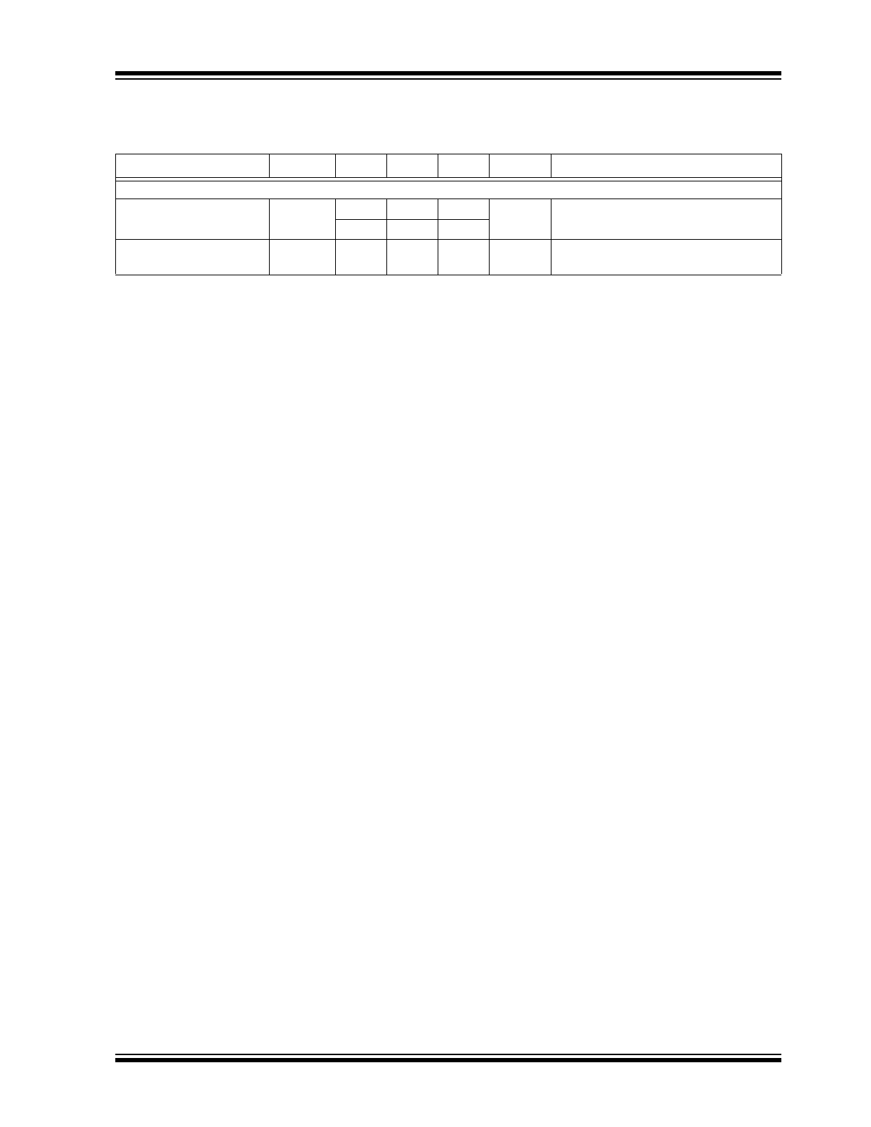
TEMPERATURE SPECIFICATIONS (
Note 1
)
Parameters
Sym.
Min.
Typ.
Max.
Units
Conditions
Temperature Ranges
Storage Temperature Range
T
J
–40
—
+125
°C
—
Lead Temperature
—
—
—
+260
°C
Soldering, 5 sec.
Package Thermal Resistance
Thermal Resistance SOT-223
θ
JC
—
15
—
°C/W
See
Thermal
Considerations Layout
for more information.
θ
JA
—
62
—
Thermal Resistance 8-Ld SOIC
θ
JA
—
160
—
°C/W
See
Thermal
Considerations Layout
for more information.
Note 1: The maximum allowable power dissipation is a function of ambient temperature, the maximum allowable
junction temperature and the thermal resistance from junction to air (i.e., T
A
, T
J
,
JA
). Exceeding the
maximum allowable power dissipation will cause the device operating junction temperature to exceed the
maximum +125°C rating. Sustained junction temperatures above +125°C can impact the device reliability.
2017 Microchip Technology Inc.
DS20005718A-page 7
MIC5201
2.0
TYPICAL PERFORMANCE CURVES
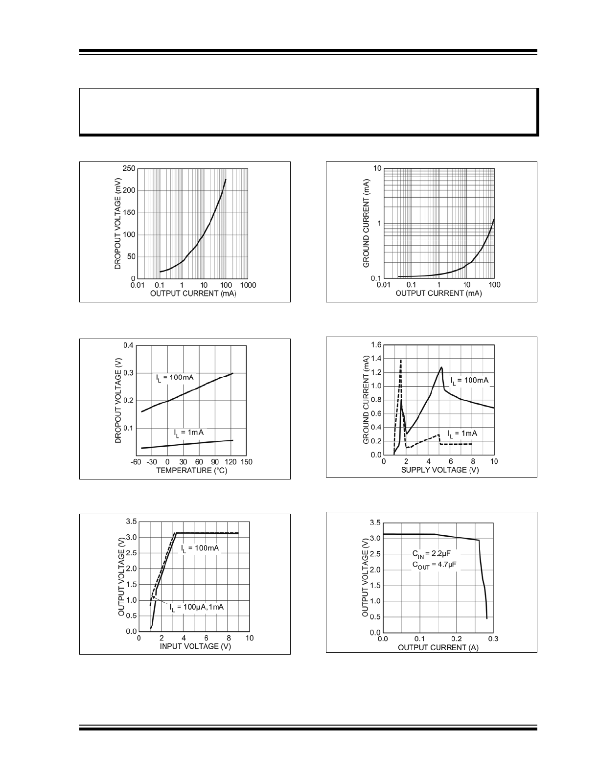
FIGURE 2-1:
Dropout Voltage vs. Output
Current.
FIGURE 2-2:
Dropout Voltage vs.
Temperature.
FIGURE 2-3:
Dropout Characteristics.
FIGURE 2-4:
Ground Current vs. Output
Current.
FIGURE 2-5:
Ground Current vs. Supply
Voltage.
FIGURE 2-6:
Output Voltage vs. Output
Current.
Note:
The graphs and tables provided following this note are a statistical summary based on a limited number of
samples and are provided for informational purposes only. The performance characteristics listed herein
are not tested or guaranteed. In some graphs or tables, the data presented may be outside the specified
operating range (e.g., outside specified power supply range) and therefore outside the warranted range.
MIC5201
DS20005718A-page 8
2017 Microchip Technology Inc.
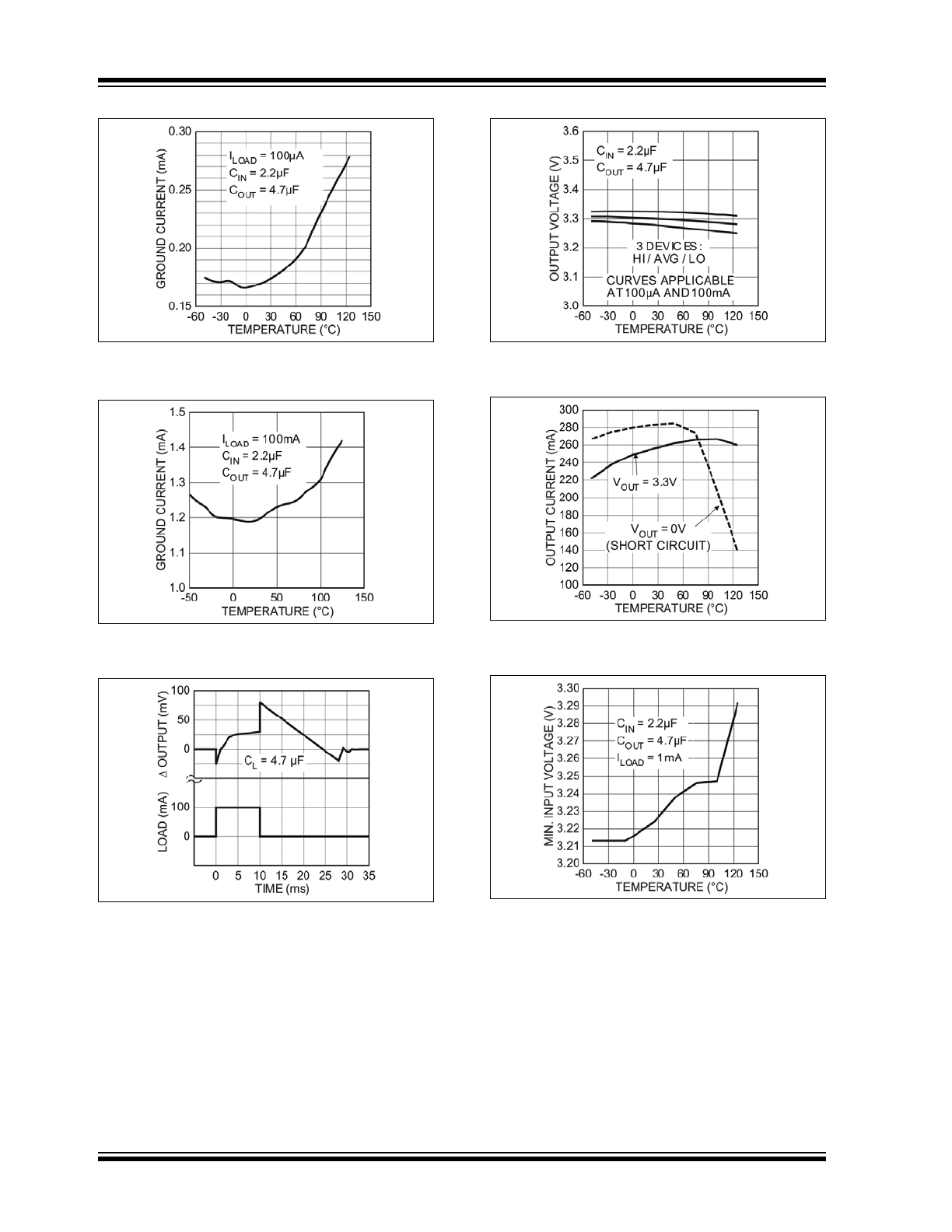
FIGURE 2-7:
Ground Current vs.
Temperature.
FIGURE 2-8:
Ground Current vs.
Temperature.
FIGURE 2-9:
Thermal Regulation (3.3V
Version).
FIGURE 2-10:
Output Voltage vs.
Temperature (3.3V Version).
FIGURE 2-11:
Output Current vs.
Temperature.
FIGURE 2-12:
Minimum Input Voltage vs.
Temperature.
2017 Microchip Technology Inc.
DS20005718A-page 9
MIC5201
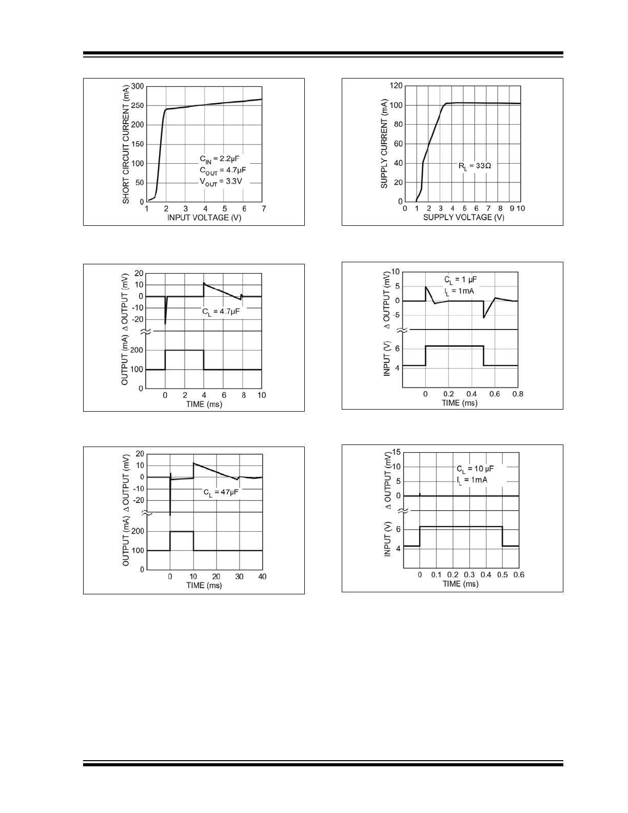
FIGURE 2-13:
Short-Circuit Current vs.
Input Voltage.
FIGURE 2-14:
Load Transient.
FIGURE 2-15:
Load Transient.
FIGURE 2-16:
Supply Current vs. Supply
Voltage (3.3V Version).
FIGURE 2-17:
Line Transient.
FIGURE 2-18:
Line Transient.
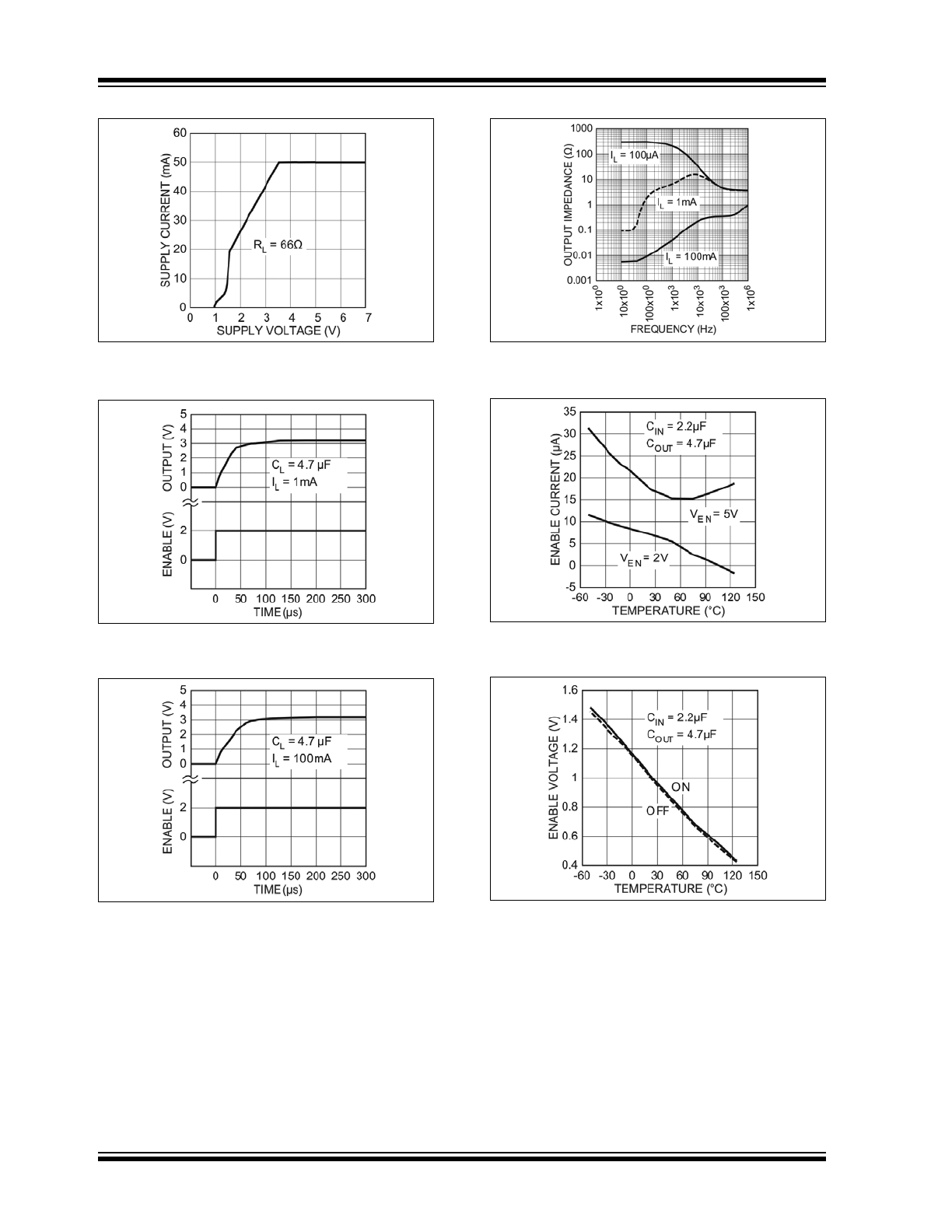
MIC5201
DS20005718A-page 10
2017 Microchip Technology Inc.
FIGURE 2-19:
Supply Current vs. Supply
Voltage (3.3V Version).
FIGURE 2-20:
Enable Transient (3.3V
Version).
FIGURE 2-21:
Enable Transient (3.3V
Version).
FIGURE 2-22:
Output Impedance.
FIGURE 2-23:
Enable Current Threshold
vs. Temperature.
FIGURE 2-24:
Enable Voltage Threshold
vs. Temperature.