
© 2009 Microchip Technology Inc.
DS22145A-page 1
MCP6L71/1R/2/4
Features
• Gain Bandwidth Product: 2 MHz (typical)
• Supply Current: I
Q
= 150 µA (typical)
• Supply Voltage: 2.0V to 6.0V
• Rail-to-Rail Input/Output
• Extended Temperature Range: –40°C to +125°C
• Available in Single, Dual and Quad Packages
Typical Applications
• Portable Equipment
• Photodiode Amplifier
• Analog Filters
• Notebooks and PDAs
• Battery Powered Systems
Design Aids
• FilterLab
®
Software
• MAPS (Microchip Advanced Part Selector)
• Analog Demonstration and Evaluation Boards
• Application Notes
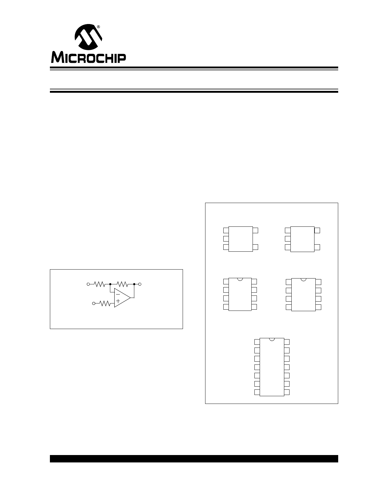
Typical Application
Description
The Microchip Technology Inc. MCP6L71/1R/2/4 family
of operational amplifiers (op amps) supports general
purpose applications. The combination of rail-to-rail
input and output, low quiescent current and bandwidth
fit into many applicaitons.
This family has a 2 MHz Gain Bandwidth Product
(GBWP) and a low 150 µA per amplifier quiescent cur-
rent. These op amps operate on supply voltages
between 2.0V and 6.0V, with rail-to-rail input and output
swing. They are available in the extended temperature
range.
Package Types
Inverting Amplifier
MCP6L71
R
1
R
2
V
REF
V
IN
V
OUT
R
3
V
IN
–
MCP6L71
SOIC, MSOP
V
DD
1
2
3
4
8
7
6
5 NC
NC
NC
V
IN
+
V
SS
V
OUT
V
INA
–
MCP6L72
SOIC, MSOP
V
OUTB
1
2
3
4
8
7
6
5 V
INB
+
V
DD
V
OUTA
V
INA
+
V
SS
V
INB
–
V
INA
–
MCP6L74
SOIC, TSSOP
V
IND
–
1
2
3
4
14
13
12
11 V
SS
V
OUTD
V
OUTA
V
INA
+
V
DD
V
IND
+
5
6
7
10
9
8
V
INB
+
V
INC
+
V
OUTC
V
INB
–
V
OUTB
V
INC
–
V
SS
MCP6L71
SOT-23-5
1
2
3
5
4
V
DD
V
OUT
V
IN
+
V
IN
–
V
DD
MCP6L71R
SOT-23-5
1
2
3
5
4
V
SS
V
OUT
V
IN
+
V
IN
–
2 MHz, 150 µA Op Amps

MCP6L71/1R/2/4
DS22145A-page 2
© 2009 Microchip Technology Inc.
NOTES:
© 2009 Microchip Technology Inc.
DS22145A-page 3
MCP6L71/1R/2/4
1.0
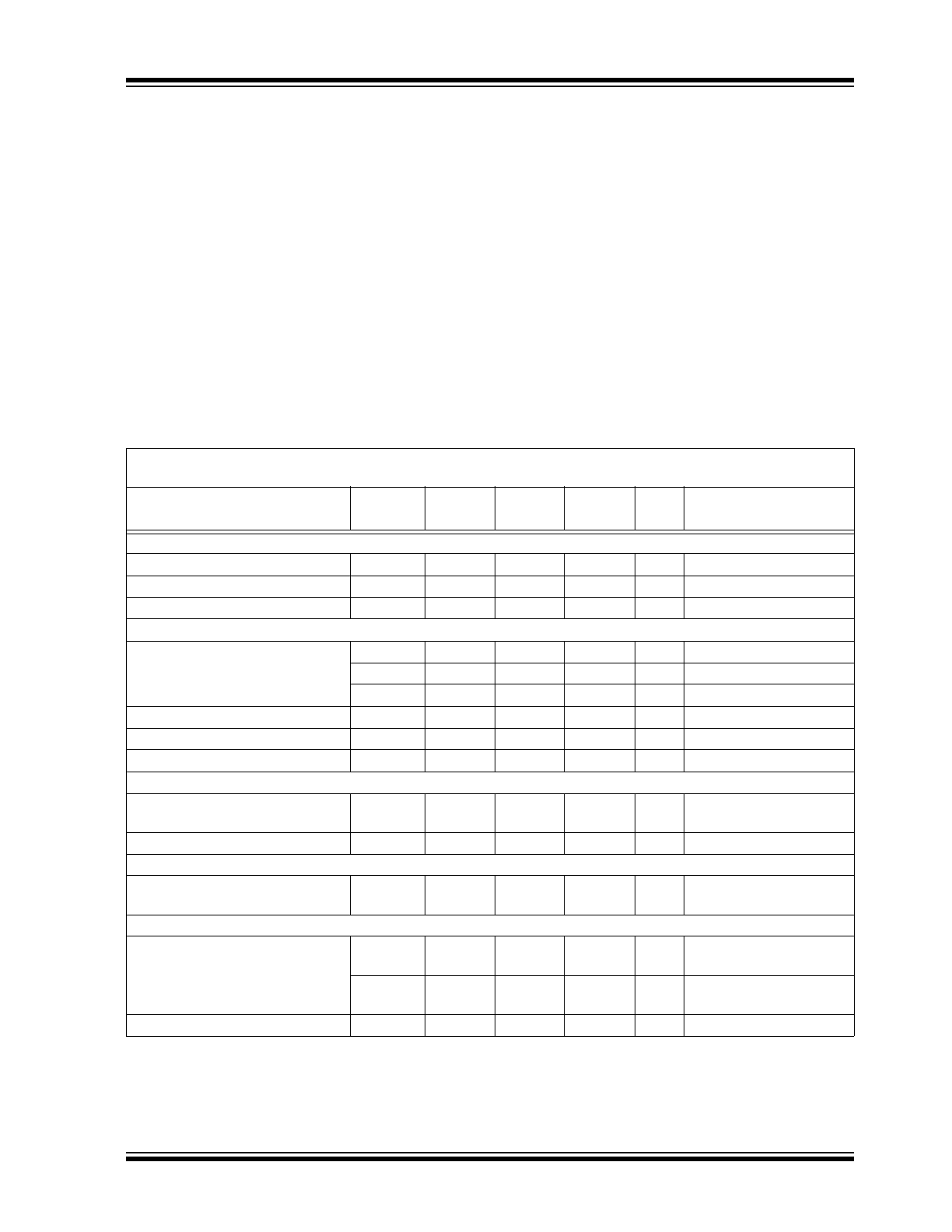
ELECTRICAL CHARACTERISTICS
1.1
Absolute Maximum Ratings †
V
DD
– V
SS
........................................................................7.0V
Current at Input Pins ....................................................±2 mA
Analog Inputs (V
IN
+ and V
IN
–) †† .. V
SS
– 1.0V to V
DD
+ 1.0V
All other Inputs and Outputs .......... V
SS
– 0.3V to V
DD
+ 0.3V
Difference Input Voltage ...................................... |V
DD
– V
SS
|
Output Short Circuit Current ................................ Continuous
Current at Output and Supply Pins ............................±30 mA
Storage Temperature ................................... –65°C to +150°C
Junction Temperature (T
J
) .........................................+150°C
ESD Protection On All Pins (HBM/MM)
................ ≥ 4 kV/400V
† Notice: Stresses above those listed under “Absolute
Maximum Ratings” may cause permanent damage to the
device. This is a stress rating only and functional operation of
the device at those or any other conditions above those
indicated in the operational listings of this specification is not
implied. Exposure to maximum rating conditions for extended
periods may affect device reliability.
†† See Section 4.1.2 “Input Voltage and Current Limits”.
1.2
Specifications
TABLE 1-1:
DC ELECTRICAL SPECIFICATIONS
Electrical Characteristics: Unless otherwise indicated, T
A
= +25°C, V
DD
= 5.0V, V
SS
= GND, V
CM
= V
DD
/2,
V
OUT
≈ V
DD
/2, V
L
= V
DD
/2 and R
L
= 10 k
Ω to V
L
. (Refer to
Figure 1-1
).
Parameters
Sym
Min
(Note 1)
Typ
Max
(Note 1)
Units
Conditions
Input Offset
Input Offset Voltage
V
OS
–4
±1
+4
mV
Input Offset Temperature Drift
ΔV
OS
/
ΔT
A
—
±1.3
—
µV/°C T
A
= –40°C to +125°C,
Power Supply Rejection Ratio
PSRR
—
89
—
dB
Input Bias Current and Impedance
Input Bias Current
I
B
—
1
—
pA
I
B
—
50
—
pA
T
A
= +85°C
I
B
—
2000
—
pA
T
A
= +125°C
Input Offset Current
I
OS
—
±1
—
pA
Common Mode Input Impedance
Z
CM
—
10
13
||6
—
Ω||pF
Differential Input Impedance
Z
DIFF
—
10
13
||3
—
Ω||pF
Common Mode
Common Mode Input Voltage
Range
V
CMR
-0.3
—
+5.3
V
Common Mode Rejection Ratio
CMRR
—
91
—
dB
V
CM
= –0.3V to 5.3V
Open-Loop Gain
DC Open-Loop Gain
(Large Signal)
A
OL
—
105
—
dB
V
OUT
= 0.2V to 4.8V,
V
CM
= V
SS
Output
Maximum Output Voltage Swing
V
OL
—
—
0.020
V
G = +2 V/V,
0.5V input overdrive
V
OH
4.980
—
—
V
G = +2 V/V,
0.5V input overdrive
Output Short Circuit Current
I
SC
—
±25
—
mA
Note 1:
For design guidance only; not tested.
MCP6L71/1R/2/4
DS22145A-page 4
© 2009 Microchip Technology Inc.
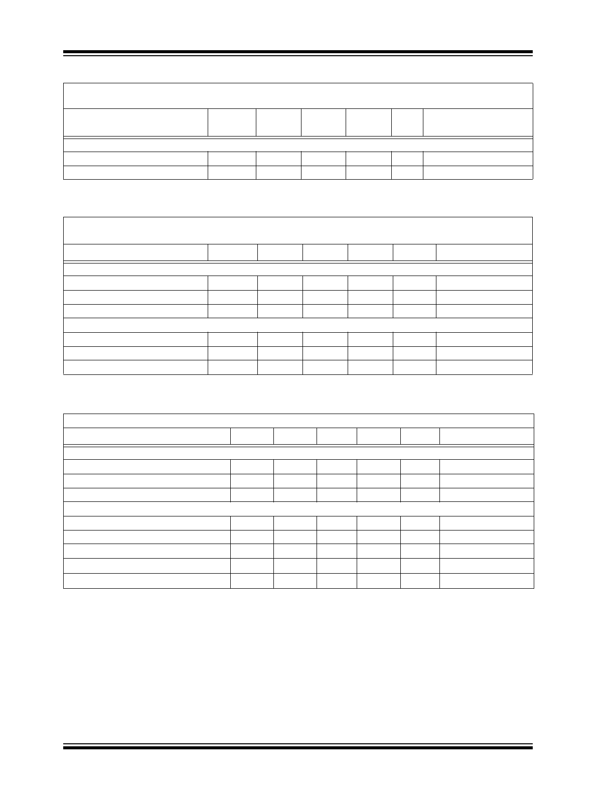
TABLE 1-2:
AC ELECTRICAL SPECIFICATIONS
TABLE 1-3:
TEMPERATURE SPECIFICATIONS
Power Supply
Supply Voltage
V
DD
2.0
—
6.0
V
Quiescent Current per Amplifier
I
Q
50
150
240
µA
I
O
= 0
Electrical Characteristics: Unless otherwise indicated, T
A
= +25°C, V
DD
= +2.0V to +5.5V, V
SS
= GND,
V
CM
= V
DD
2, V
OUT
≈ V
DD
/2, V
L
= V
DD
/2, R
L
= 10 k
Ω to V
L
and C
L
= 60 pF. (Refer to
Figure 1-1
).
Parameters
Sym
Min
Typ
Max
Units
Conditions
AC Response
Gain Bandwidth Product
GBWP
—
2.0
—
MHz
Phase Margin
PM
—
65
—
°
G = +1 V/V
Slew Rate
SR
—
0.9
—
V/µs
Noise
Input Noise Voltage
E
ni
—
4.6
—
µV
P-P
f = 0.1 Hz to 10 Hz
Input Noise Voltage Density
e
ni
—
19
—
nV/
√Hz f = 10 kHz
Input Noise Current Density
i
ni
—
3
—
fA/
√Hz f = 1 kHz
TABLE 1-1:
DC ELECTRICAL SPECIFICATIONS (CONTINUED)
Electrical Characteristics: Unless otherwise indicated, T
A
= +25°C, V
DD
= 5.0V, V
SS
= GND, V
CM
= V
DD
/2,
V
OUT
≈ V
DD
/2, V
L
= V
DD
/2 and R
L
= 10 k
Ω to V
L
. (Refer to
Figure 1-1
).
Parameters
Sym
Min
(Note 1)
Typ
Max
(Note 1)
Units
Conditions
Note 1:
For design guidance only; not tested.
Electrical Characteristics: Unless otherwise indicated, V
DD
= +2.0V to +5.5V and V
SS
= GND.
Parameters
Sym
Min
Typ
Max
Units
Conditions
Temperature Ranges
Specified Temperature Range
T
A
–40
—
+125
°C
Operating Temperature Range
T
A
–40
—
+125
°C
Note 1
Storage Temperature Range
T
A
–65
—
+150
°C
Thermal Package Resistances
Thermal Resistance, 5L-SOT-23
θ
JA
—
256
—
°C/W
Thermal Resistance, 8L-SOIC
θ
JA
—
163
—
°C/W
Thermal Resistance, 8L-MSOP
θ
JA
—
206
—
°C/W
Thermal Resistance, 14L-SOIC
θ
JA
—
120
—
°C/W
Thermal Resistance, 14L-TSSOP
θ
JA
—
100
—
°C/W
Note 1: The Junction Temperature (T
J
) must not exceed the Absolute Maximum specification of +150°C.
© 2009 Microchip Technology Inc.
DS22145A-page 5
MCP6L71/1R/2/4
1.3
Test Circuits
The circuit used for most DC and AC tests is shown in
Figure 1-1
. This circuit can independently set V
CM
and
V
OUT
; see
Equation 1-1
. Note that V
CM
is not the
circuit’s common mode voltage ((V
P
+ V
M
)/2), and that
V
OST
includes V
OS
plus the effects (on the input offset
error, V
OST
) of temperature, CMRR, PSRR and A
OL
.
EQUATION 1-1:
FIGURE 1-1:
AC and DC Test Circuit for
Most Specifications.
G
DM
R
F
R
G
⁄
=
V
CM
V
P
V
DD
2
⁄
+
(
) 2
⁄
=
V
OUT
V
DD
2
⁄
(
)
V
P
V
M
–
(
) V
OST
1
G
DM
+
(
)
+
+
=
Where:
G
DM
= Differential Mode Gain
(V/V)
V
CM
= Op Amp’s Common Mode
Input Voltage
(V)
V
OST
= Op Amp’s Total Input Offset
Voltage
(mV)
V
OST
V
IN–
V
IN+
–
=
V
DD
MCP6L7X
R
G
R
F
V
OUT
V
M
C
B2
C
L
R
L
V
L
C
B1
100 k
Ω
100 k
Ω
R
G
R
F
V
DD
/2
V
P
100 k
Ω
100 k
Ω
60 pF
10 k
Ω
1 µF
100 nF
V
IN–
V
IN+
C
F
6.8 pF
C
F
6.8 pF

MCP6L71/1R/2/4
DS22145A-page 6
© 2009 Microchip Technology Inc.
NOTES:
© 2009 Microchip Technology Inc.
DS22145A-page 7
MCP6L71/1R/2/4
2.0
TYPICAL PERFORMANCE CURVES
Note: Unless otherwise indicated, T
A
= +25°C, V
DD
= 5.0V, V
SS
= GND, V
CM
= V
DD
/2, V
OUT
≈ V
DD
/2, V
L
= V
DD
/2,
R
L
= 10 k
Ω to V
L
and C
L
= 60 pF.
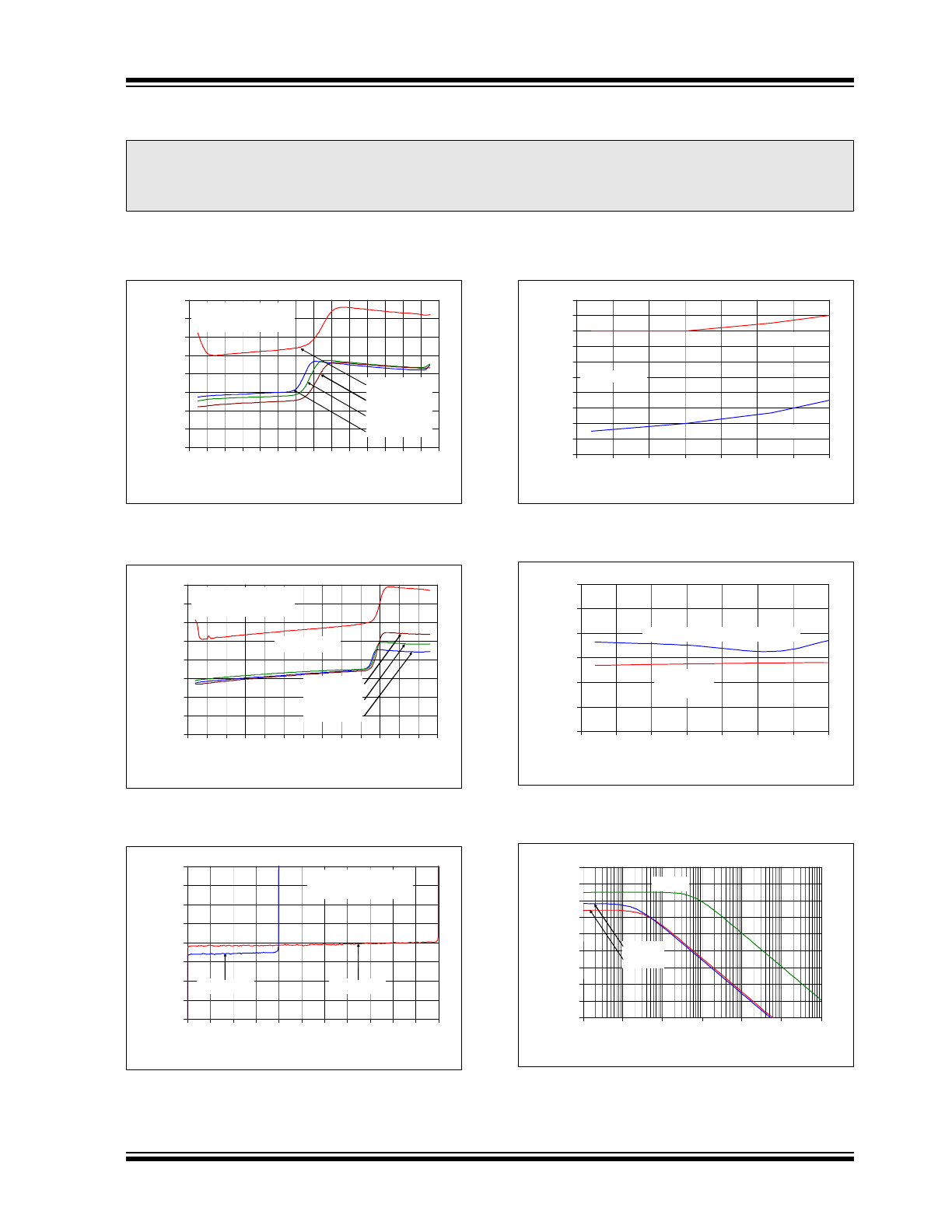
FIGURE 2-1:
Input Offset Voltage vs.
Common Mode Input Voltage at V
DD
= 2.0V.
FIGURE 2-2:
Input Offset Voltage vs.
Common Mode Input Voltage at V
DD
= 5.5V.
FIGURE 2-3:
Input Offset Voltage vs.
Output Voltage.
FIGURE 2-4:
Input Common Mode Range
Voltage vs. Ambient Temperature.
FIGURE 2-5:
CMRR, PSRR vs.
Temperature.
FIGURE 2-6:
CMRR, PSRR vs.
Frequency.
Note:
The graphs and tables provided following this note are a statistical summary based on a limited number of
samples and are provided for informational purposes only. The performance characteristics listed herein
are not tested or guaranteed. In some graphs or tables, the data presented may be outside the specified
operating range (e.g., outside specified power supply range) and therefore outside the warranted range.
-100
-50
0
50
100
150
200
250
300
-0
.4
-0
.2
0.
0
0.
2
0.
4
0.
6
0.
8
1.
0
1.
2
1.
4
1.
6
1.
8
2.
0
2.
2
2.
4
Common Mode Input Voltage (V)
In
p
u
t O
ffs
e
t V
o
lt
a
g
e
(µ
V
)
V
DD
= 2.0V
Representitive Part
T
A
= +125°C
T
A
= +85°C
T
A
= +25°C
T
A
= -40°C
-100
-50
0
50
100
150
200
250
300
-0
.5
0.
0
0.
5
1.
0
1.
5
2.
0
2.
5
3.
0
3.
5
4.
0
4.
5
5.
0
5.
5
6.
0
Common Mode Input Voltage (V)
Input
O
ff
s
e
t V
o
lt
a
g
e
(
µ
V
)
V
DD
= 5.5V
Representitive Part
T
A
= +85°C
T
A
= +25°C
T
A
= -40°C
T
A
= +125°C
-100
-50
0
50
100
150
200
250
300
0.0 0.5 1.0 1.5 2.0 2.5 3.0 3.5 4.0 4.5 5.0 5.5
Output Voltage (V)
In
p
u
t O
ffs
e
t V
o
lt
a
g
e
(µ
V
)
V
DD
= 2.0V
V
CM
= V
SS
Representative Part
V
DD
= 5.5V
-0.5
-0.4
-0.3
-0.2
-0.1
0.0
0.1
0.2
0.3
0.4
0.5
-50
-25
0
25
50
75
100
125
Ambient Temperature (°C)
C
o
m
m
on
M
o
d
e
R
a
ng
e
(
V
)
V
CMRH
– V
DD
V
CMRL
– V
SS
One Wafer Lot
60
70
80
90
100
110
120
-50
-25
0
25
50
75
100
125
Ambient Temperature (°C)
P
S
RR
, CM
RR (dB)
PSRR
(V
CM
= V
SS
)
CMRR (V
CM
= -0.3V to +5.3V)
20
30
40
50
60
70
80
90
100
110
1.E+00 1.E+01 1.E+02 1.E+03 1.E+04 1.E+05 1.E+06
Frequency (Hz)
CM
RR,
P
S
RR
(d
B)
1
10k
100k
1M
100
10
1k
PSRR–
PSRR+
CMRR
MCP6L71/1R/2/4
DS22145A-page 8
© 2009 Microchip Technology Inc.
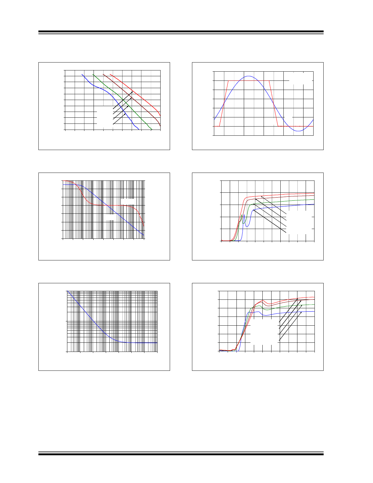
Note: Unless otherwise indicated, T
A
= +25°C, V
DD
= 5.0V, V
SS
= GND, V
CM
= V
DD
/2, V
OUT
≈ V
DD
/2, V
L
= V
DD
/2,
R
L
= 10 k
Ω to V
L
and C
L
= 60 pF.
FIGURE 2-7:
Input Current vs. Input
Voltage.
FIGURE 2-8:
Open-Loop Gain, Phase vs.
Frequency.
FIGURE 2-9:
Input Noise Voltage Density
vs. Frequency.
FIGURE 2-10:
The MCP6L71/1R/2/4 Show
No Phase Reversal.
FIGURE 2-11:
Quiescent Current vs.
Supply Voltage.
FIGURE 2-12:
Output Short Circuit Current
vs. Supply Voltage.
1.E-12
1.E-11
1.E-10
1.E-09
1.E-08
1.E-07
1.E-06
1.E-05
1.E-04
1.E-03
1.E-02
-1.0 -0.9 -0.8 -0.7 -0.6 -0.5 -0.4 -0.3 -0.2 -0.1 0.0
Input Voltage (V)
Inpu
t C
u
rr
e
n
t M
a
gn
it
u
d
e
(
A
)
+125°C
+85°C
+25°C
-40°C
10m
1m
100µ
10µ
1µ
100n
10n
1n
100p
10p
1p
-20
0
20
40
60
80
100
120
1.
E
-0
1
1.
E
+
0
0
1.E
+
01
1.
E+
02
1.
E
+
0
3
1.E
+
04
1.
E+
05
1.E+
06
1.E
+
07
Frequency (Hz)
Op
e
n
-L
o
o
p
Ga
in
(
d
B
)
-210
-180
-150
-120
-90
-60
-30
0
O
p
e
n
-L
o
o
p
P
h
as
e
(°
)
Gain
Phase
0.1
1
10
100
1k 10k 100k 1M 10M
10
100
1,000
1.E-
01
1.E+0
0
1.E+0
1
1.E+0
2
1.E+0
3
1.E+0
4
1.E+0
5
1.E+0
6
Frequency (Hz)
In
p
u
t N
o
is
e
Vo
lt
ag
e D
e
n
s
it
y
(n
V
/√
Hz
)
0.1
100
10
1k
100k
10k
1M
1
-1
0
1
2
3
4
5
6
Time (1 ms/div)
In
p
u
t,
O
u
tp
u
t
V
o
lt
ag
e
(
V
)
V
DD
= 5.0V
G = +2 V/V
V
IN
V
OUT
0
50
100
150
200
250
0.0 0.5 1.0 1.5 2.0 2.5 3.0 3.5 4.0 4.5 5.0 5.5
Power Supply Voltage (V)
Q
u
ie
sc
en
t C
u
rr
e
n
t
(µ
A
/am
p
lif
ier
)
T
A
= +125°C
T
A
= +85°C
T
A
= +25°C
T
A
= -40°C
0
5
10
15
20
25
30
35
0.0 0.5 1.0 1.5 2.0 2.5 3.0 3.5 4.0 4.5 5.0 5.5
Power Supply Voltage (V)
O
u
p
tut S
h
or
t-C
ir
c
u
it
Cu
rr
e
n
t
(m
A)
T
A
= +125°C
T
A
= +85°C
T
A
= +25°C
T
A
= -40°C
© 2009 Microchip Technology Inc.
DS22145A-page 9
MCP6L71/1R/2/4
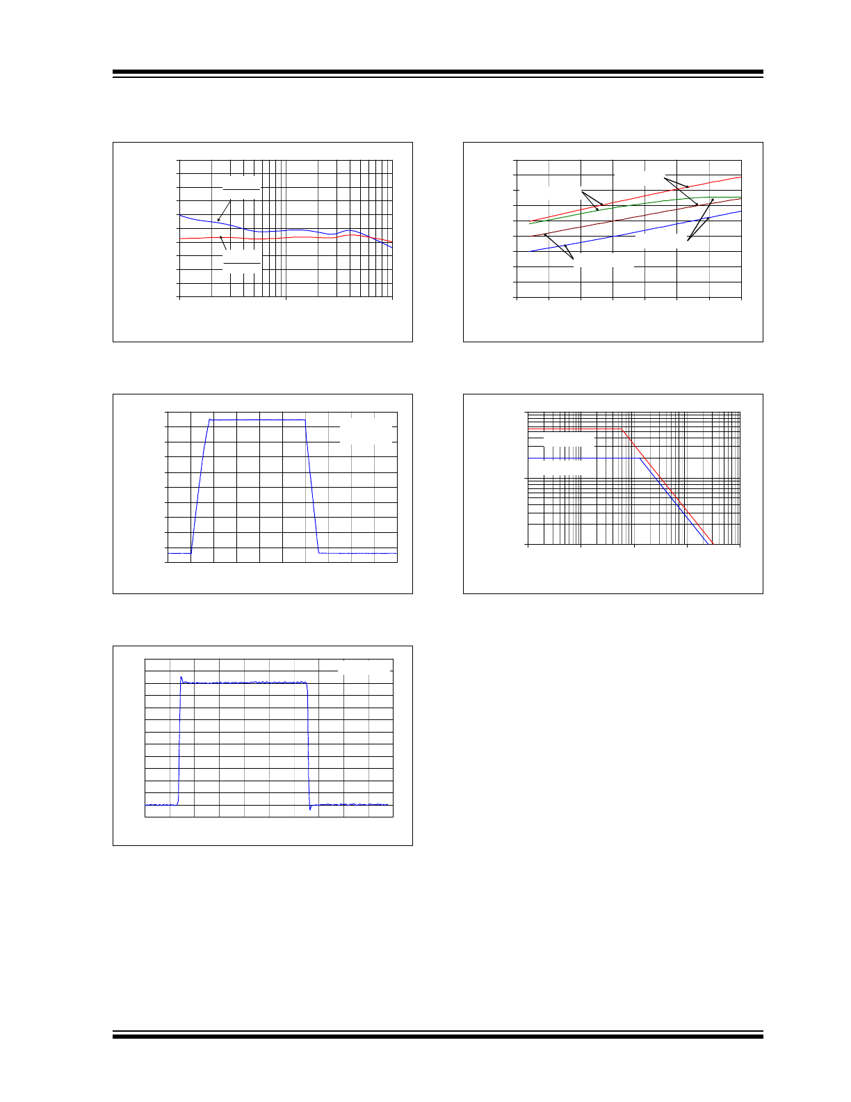
Note: Unless otherwise indicated, T
A
= +25°C, V
DD
= 5.0V, V
SS
= GND, V
CM
= V
DD
/2, V
OUT
≈ V
DD
/2, V
L
= V
DD
/2,
R
L
= 10 k
Ω to V
L
and C
L
= 60 pF.
FIGURE 2-13:
Ratio of Output Voltage
Headroom vs. Output Current Magnitude.
FIGURE 2-14:
Large Signal Non-inverting
Pulse Response.
FIGURE 2-15:
Small Signal Non-inverting
Pulse Response.
FIGURE 2-16:
Slew Rate vs. Ambient
Temperature.
FIGURE 2-17:
Maximum Output Voltage
Swing vs. Frequency.
0
5
10
15
20
25
30
35
40
45
50
0.1
1
10
Output Current Magnitude (mA)
Ra
ti
o
o
f
O
u
tp
u
t He
a
d
ro
om
to
O
u
tp
u
t Cu
rr
e
n
t (m
V
/m
A
)
V
DD
– V
OH
I
OUT
V
OL
– V
SS
-I
OUT
0.0
0.5
1.0
1.5
2.0
2.5
3.0
3.5
4.0
4.5
5.0
Time (5 µs/div)
Ou
tp
u
t V
o
lt
a
g
e
(
V
)
G = +1 V/V
V
DD
= 5.0V
Time (2 µs/div)
O
u
tp
u
t Vo
lt
a
g
e
(
1
0
m
V
/d
iv
)
G = +1 V/V
0.0
0.2
0.4
0.6
0.8
1.0
1.2
1.4
1.6
1.8
-50
-25
0
25
50
75
100
125
Ambient Temperature (°C)
Sl
e
w
R
a
te
(
V
/µ
s
)
Falling Edge
V
DD
= 5.5V
V
DD
= 2.0V
Rising Edge
0.1
1
10
1.E
+
03
1.E+
04
1.
E+
05
1.E
+
06
1.
E+
07
Frequency (Hz)
M
a
xi
m
u
m
O
u
tp
u
t
V
o
lt
a
g
e
Sw
in
g
(
V
P-
P
)
V
DD
= 2.0V
1k
10k
100k
1M
V
DD
= 5.5V
10M

MCP6L71/1R/2/4
DS22145A-page 10
© 2009 Microchip Technology Inc.
NOTES: