
© 2007 Microchip Technology Inc.
DS21314G-page 1
MCP601/1R/2/3/4
Features
• Single-Supply: 2.7V to 6.0V
• Rail-to-Rail Output
• Input Range Includes Ground
• Gain Bandwidth Product: 2.8 MHz (typical)
• Unity-Gain Stable
• Low Quiescent Current: 230 µA/amplifier (typical)
• Chip Select (CS):
MCP603 only
• Temperature Ranges:
- Industrial: -40°C to +85°C
- Extended: -40°C to +125°C
• Available in Single, Dual, and Quad
Typical Applications
• Portable Equipment
• A/D Converter Driver
• Photo Diode Pre-amp
• Analog Filters
• Data Acquisition
• Notebooks and PDAs
• Sensor Interface
Available Tools
• SPICE Macro Models
• FilterLab
®
Software
• Mindi™ Simulation Tool
• MAPS (Microchip Advanced Part Selector)
• Analog Demonstration and Evaluation Boards
• Application Notes
Description
The Microchip Technology Inc. MCP601/1R/2/3/4
family of low-power operational amplifiers (op amps)
are offered in single (MCP601), single with Chip Select
(CS) (MCP603), dual (MCP602), and quad (MCP604)
configurations. These op amps utilize an advanced
CMOS technology that provides low bias current, high-
speed operation, high open-loop gain, and rail-to-rail
output swing. This product offering operates with a
single supply voltage that can be as low as 2.7V, while
drawing 230 µA (typical) of quiescent current per
amplifier. In addition, the common mode input voltage
range goes 0.3V below ground, making these
amplifiers ideal for single-supply operation.
These devices are appropriate for low power, battery
operated circuits due to the low quiescent current, for
A/D convert driver amplifiers because of their wide
bandwidth or for anti-aliasing filters by virtue of their low
input bias current.
The MCP601, MCP602, and MCP603 are available in
standard 8-lead PDIP, SOIC, and TSSOP packages.
The MCP601 and MCP601R are also available in a
standard 5-lead SOT-23 package, while the MCP603 is
available in a standard 6-lead SOT-23 package. The
MCP604 is offered in standard 14-lead PDIP, SOIC,
and TSSOP packages.
The MCP601/1R/2/3/4 family is available in the
Industrial and Extended temperature ranges and has a
power supply range of 2.7V to 6.0V.
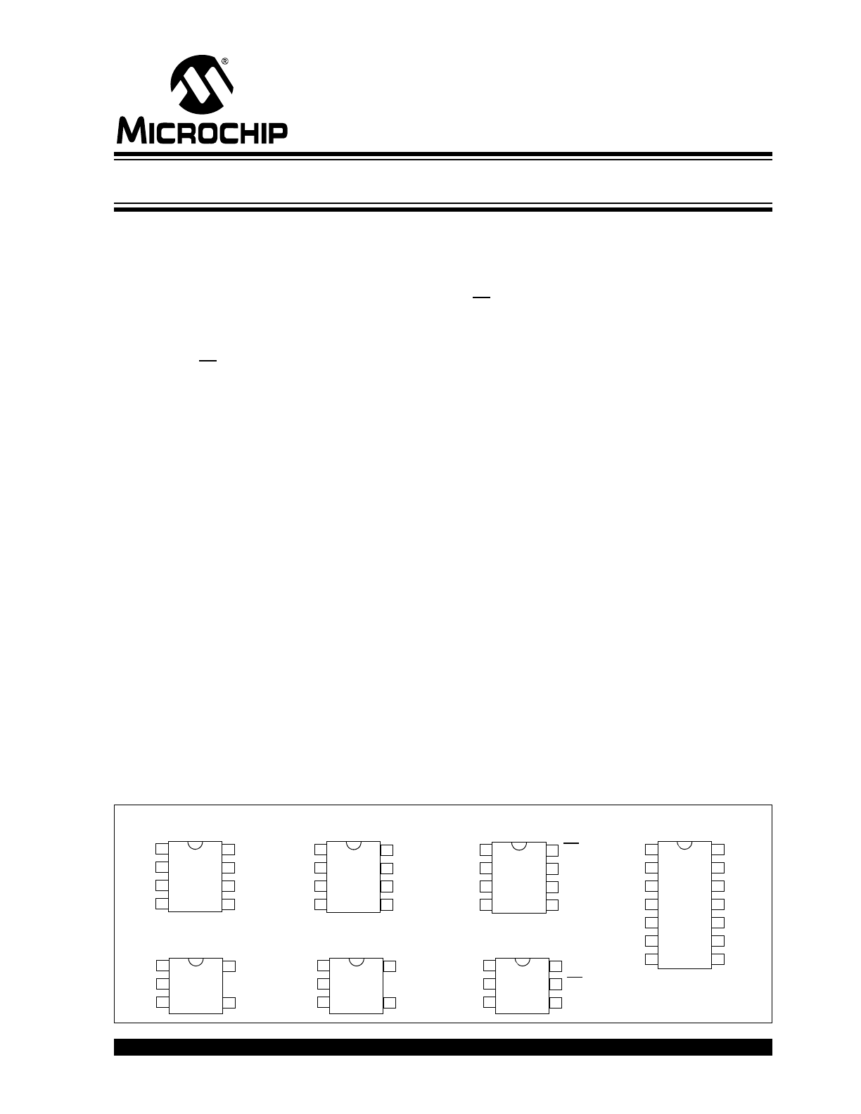
Package Types
V
IN
+
V
IN
–
V
SS
V
OUT
V
DD
1
2
3
4
8
7
6
5
NC
NC
NC
V
INA
+
V
INA
–
V
DD
V
INC
+
V
SS
V
OUTC
V
INC
–
V
OUTA
V
INB
+
V
IND
–
V
OUTD
V
OUTB
V
INB
–
V
IND
+
V
INA
+
V
INA
–
V
SS
V
INB
–
V
OUTB
1
2
3
4
8
7
6
5
V
DD
V
INB
+
V
OUTA
MCP601
PDIP, SOIC, TSSOP
MCP604
PDIP, SOIC, TSSOP
MCP602
PDIP, SOIC, TSSOP
V
IN
+
V
SS
V
IN
–
1
2
3
5
4
V
DD
V
OUT
MCP601
SOT23-5
V
IN
+
V
SS
V
IN
–
1
2
3
6
4
V
DD
V
OUT
MCP603
SOT23-6
CS
5
V
IN
+
V
IN
–
V
SS
V
OUT
V
DD
1
2
3
4
8
7
6
5
CS
NC
NC
MCP603
PDIP, SOIC, TSSOP
14
13
12
1
2
3
4
5
6
7
11
10
9
8
V
IN
+
V
DD
V
IN
–
1
2
3
5
4
V
SS
V
OUT
MCP601R
SOT23-5
2.7V to 6.0V Single Supply CMOS Op Amps
MCP601/1R/2/3/4
DS21314G-page 2
© 2007 Microchip Technology Inc.
1.0
ELECTRICAL
CHARACTERISTICS
Absolute Maximum Ratings †
V
DD
– V
SS
........................................................................7.0V
Current at Input Pins .....................................................±2 mA
Analog Inputs (V
IN
+, V
IN
–)
†† ........ V
SS
– 1.0V to V
DD
+ 1.0V
All Other Inputs and Outputs ......... V
SS
– 0.3V to V
DD
+ 0.3V
Difference Input Voltage ...................................... |V
DD
– V
SS
|
Output Short Circuit Current .................................Continuous
Current at Output and Supply Pins ............................±30 mA
Storage Temperature.................................... –65°C to +150°C
Maximum Junction Temperature (T
J
) ......................... .+150°C
ESD Protection On All Pins (HBM; MM)
.............. ≥ 3 kV; 200V
† Notice: Stresses above those listed under “Absolute
Maximum Ratings” may cause permanent damage to the
device. This is a stress rating only and functional operation of
the device at those or any other conditions above those
indicated in the operational listings of this specification is not
implied. Exposure to maximum rating conditions for extended
periods may affect device reliability.
†† See Section 4.1.2 “Input Voltage and Current Limits”.
DC CHARACTERISTICS
Electrical Specifications: Unless otherwise specified, T
A
= +25°C, V
DD
= +2.7V to +5.5V, V
SS
= GND, V
CM
= V
DD
/2,
V
OUT
≈ V
DD
/2, V
L
= V
DD
/2, and R
L
= 100 k
Ω to V
L
, and CS is tied low. (Refer to
Figure 1-2
and
Figure 1-3
).
Parameters
Sym
Min
Typ
Max
Units
Conditions
Input Offset
Input Offset Voltage
V
OS
-2
±0.7
+2
mV
Industrial Temperature
V
OS
-3
±1
+3
mV
T
A
= -40°C to +85°C
(Note 1)
Extended Temperature
V
OS
-4.5
±1
+4.5
mV
T
A
= -40°C to +125°C
(Note 1)
Input Offset Temperature Drift
ΔV
OS
/
ΔT
A
—
±2.5
—
µV/°C T
A
= -40°C to +125°C
Power Supply Rejection
PSRR
80
88
—
dB
V
DD
= 2.7V to 5.5V
Input Current and Impedance
Input Bias Current
I
B
—
1
—
pA
Industrial Temperature
I
B
—
20
60
pA
T
A
= +85°C
(Note 1)
Extended Temperature
I
B
—
450
5000
pA
T
A
= +125°C
(Note 1)
Input Offset Current
I
OS
—
±1
—
pA
Common Mode Input Impedance
Z
CM
—
10
13
||6
—
Ω||pF
Differential Input Impedance
Z
DIFF
—
10
13
||3
—
Ω||pF
Common Mode
Common Mode Input Range
V
CMR
V
SS
– 0.3
—
V
DD
– 1.2
V
Common Mode Rejection Ratio
CMRR
75
90
—
dB
V
DD
= 5.0V, V
CM
= -0.3V to 3.8V
Open-loop Gain
DC Open-loop Gain (large signal)
A
OL
100
115
—
dB
R
L
= 25 k
Ω to V
L
,
V
OUT
= 0.1V to V
DD
– 0.1V
A
OL
95
110
—
dB
R
L
= 5 k
Ω to V
L
,
V
OUT
= 0.1V to V
DD
– 0.1V
Output
Maximum Output Voltage Swing
V
OL
, V
OH
V
SS
+ 15
—
V
DD
– 20
mV
R
L
= 25 k
Ω to V
L
, Output overdrive = 0.5V
V
OL
, V
OH
V
SS
+ 45
—
V
DD
– 60
mV
R
L
= 5 k
Ω to V
L
, Output overdrive = 0.5V
Linear Output Voltage Swing
V
OUT
V
SS
+ 100
—
V
DD
– 100
mV
R
L
= 25 k
Ω to V
L
, A
OL
≥ 100 dB
V
OUT
V
SS
+ 100
—
V
DD
– 100
mV
R
L
= 5 k
Ω to V
L
, A
OL
≥ 95 dB
Output Short Circuit Current
I
SC
—
±22
—
mA
V
DD
= 5.5V
I
SC
—
±12
—
mA
V
DD
= 2.7V
Power Supply
Supply Voltage
V
DD
2.7
—
6.0
V
(Note 2)
Quiescent Current per Amplifier
I
Q
—
230
325
µA
I
O
= 0
Note 1:
These specifications are not tested in either the SOT-23 or TSSOP packages with date codes older than YYWW = 0408.
In these cases, the minimum and maximum values are by design and characterization only.
2:
All parts with date codes November 2007 and later have been screened to ensure operation at V
DD
=6.0V. However, the
other minimum and maximum specifications are measured at 1.4V and/or 5.5V.
© 2007 Microchip Technology Inc.
DS21314G-page 3
MCP601/1R/2/3/4
AC CHARACTERISTICS
MCP603 CHIP SELECT (CS) CHARACTERISTICS
FIGURE 1-1:
MCP603 Chip Select (CS)
Timing Diagram.
Electrical Specifications: Unless otherwise indicated, T
A
= +25°C, V
DD
= +2.7V to +5.5V, V
SS
= GND, V
CM
= V
DD
/2,
V
OUT
≈ V
DD
/2, V
L
= V
DD
/2, and R
L
= 100 k
Ω to V
L
, C
L
= 50 pF, and CS is tied low. (Refer to
Figure 1-2
and
Figure 1-3
).
Parameters
Sym
Min
Typ
Max
Units
Conditions
Frequency Response
Gain Bandwidth Product
GBWP
—
2.8
—
MHz
Phase Margin
PM
—
50
—
°
G = +1 V/V
Step Response
Slew Rate
SR
—
2.3
—
V/µs
G = +1 V/V
Settling Time (0.01%)
t
settle
—
4.5
—
µs
G = +1 V/V, 3.8V step
Noise
Input Noise Voltage
E
ni
—
7
—
µV
P-P
f = 0.1 Hz to 10 Hz
Input Noise Voltage Density
e
ni
—
29
—
nV/
√Hz f = 1 kHz
e
ni
—
21
—
nV/
√Hz f = 10 kHz
Input Noise Current Density
i
ni
—
0.6
—
fA/
√Hz f = 1 kHz
Electrical Specifications: Unless otherwise indicated, T
A
= +25°C, V
DD
= +2.7V to +5.5V, V
SS
= GND, V
CM
= V
DD
/2,
V
OUT
≈ V
DD
/2, V
L
= V
DD
/2, and R
L
= 100 k
Ω to V
L
, C
L
= 50 pF, and CS is tied low. (Refer to
Figure 1-2
and
Figure 1-3
).
Parameters
Sym
Min
Typ
Max
Units
Conditions
CS Low Specifications
CS Logic Threshold, Low
V
IL
V
SS
—
0.2 V
DD
V
CS Input Current, Low
I
CSL
-1.0
—
—
µA
CS = 0.2V
DD
CS High Specifications
CS Logic Threshold, High
V
IH
0.8 V
DD
—
V
DD
V
CS Input Current, High
I
CSH
—
0.7
2.0
µA
CS = V
DD
Shutdown V
SS
current
I
Q_SHDN
-2.0
-0.7
—
µA
CS = V
DD
Amplifier Output Leakage in Shutdown
I
O_SHDN
—
1
—
nA
Timing
CS Low to Amplifier Output Turn-on Time
t
ON
—
3.1
10
µs
CS
≤ 0.2V
DD
, G = +1 V/V
CS High to Amplifier Output High-Z Time
t
OFF
—
100
—
ns
CS
≥ 0.8V
DD
, G = +1 V/V, No load.
Hysteresis
V
HYST
—
0.4
—
V
V
DD
= 5.0V
CS
t
OFF
V
OUT
t
ON
Hi-Z
Hi-Z
I
DD
2 nA
230 µA
Output Active
I
SS
-700 nA
-230 µA
CS
700 nA
2 nA
Current
(typical)
(typical)
(typical)
(typical)
(typical)
(typical)
MCP601/1R/2/3/4
DS21314G-page 4
© 2007 Microchip Technology Inc.
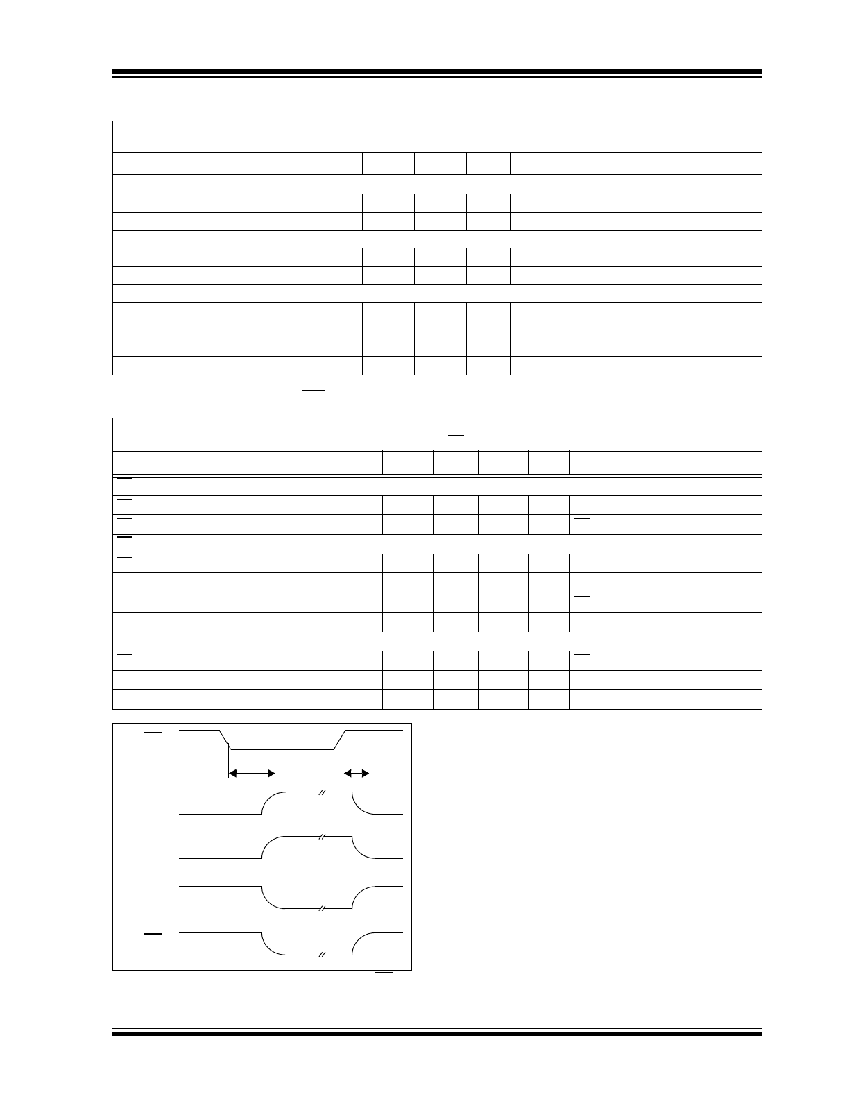
1.1
Test Circuits
The test circuits used for the DC and AC tests are
shown in
Figure 1-2
and
Figure 1-2
. The bypass
capacitors are laid out according to the rules discussed
in
Section 4.5 “Supply Bypass”.
FIGURE 1-2:
AC and DC Test Circuit for
Most Non-Inverting Gain Conditions.
FIGURE 1-3:
AC and DC Test Circuit for
Most Inverting Gain Conditions.
TEMPERATURE CHARACTERISTICS
Electrical Specifications: Unless otherwise indicated, V
DD
= +2.7V to +5.5V and V
SS
= GND.
Parameters
Sym
Min
Typ
Max
Units
Conditions
Temperature Ranges
Specified Temperature Range
T
A
-40
—
+85
°C
Industrial temperature parts
T
A
-40
—
+125
°C
Extended temperature parts
Operating Temperature Range
T
A
-40
—
+125
°C
Note
Storage Temperature Range
T
A
-65
—
+150
°C
Thermal Package Resistances
Thermal Resistance, 5L-SOT23
θ
JA
—
256
—
°C/W
Thermal Resistance, 6L-SOT23
θ
JA
—
230
—
°C/W
Thermal Resistance, 8L-PDIP
θ
JA
—
85
—
°C/W
Thermal Resistance, 8L-SOIC
θ
JA
—
163
—
°C/W
Thermal Resistance, 8L-TSSOP
θ
JA
—
124
—
°C/W
Thermal Resistance, 14L-PDIP
θ
JA
—
70
—
°C/W
Thermal Resistance, 14L-SOIC
θ
JA
—
120
—
°C/W
Thermal Resistance, 14L-TSSOP
θ
JA
—
100
—
°C/W
Note:
The Industrial temperature parts operate over this extended range, but with reduced performance. The
Extended temperature specs do not apply to Industrial temperature parts. In any case, the internal Junction
temperature (T
J
) must not exceed the absolute maximum specification of 150°C.
V
DD
MCP60X
R
G
R
F
R
N
V
OUT
V
IN
V
DD
/2
1 µF
C
L
R
L
V
L
0.1 µF
V
DD
MCP60X
R
G
R
F
R
N
V
OUT
V
DD
/2
V
IN
1 µF
C
L
R
L
V
L
0.1 µF
© 2007 Microchip Technology Inc.
DS21314G-page 5
MCP601/1R/2/3/4
2.0
TYPICAL PERFORMANCE CURVES
Note: Unless otherwise indicated, T
A
= +25°C, V
DD
= +2.7V to +5.5V, V
SS
= GND, V
CM
= V
DD
/2, V
OUT
≈ V
DD
/2,
V
L
= V
DD
/2, R
L
= 100 k
Ω to V
L
, C
L
= 50 pF and CS is tied low.
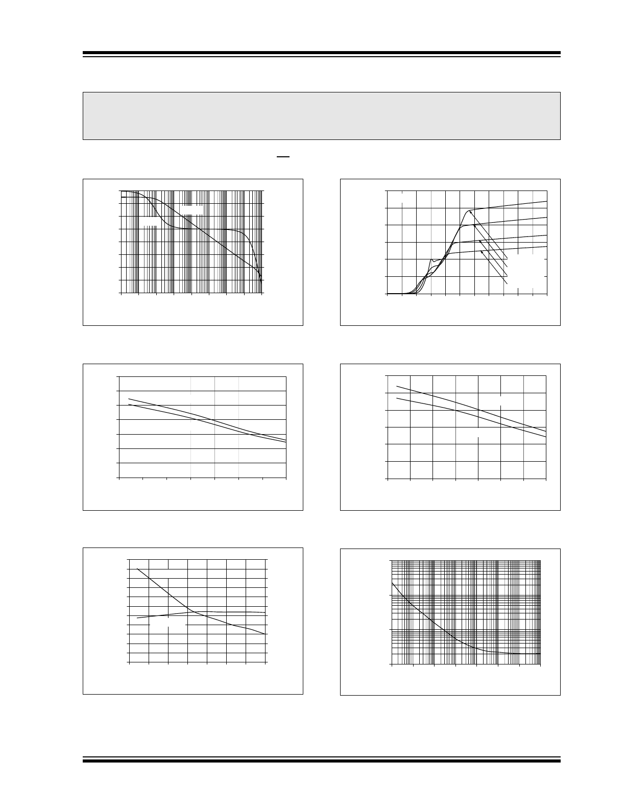
FIGURE 2-1:
Open-Loop Gain, Phase vs.
Frequency.
FIGURE 2-2:
Slew Rate vs. Temperature.
FIGURE 2-3:
Gain Bandwidth Product,
Phase Margin vs. Temperature.
FIGURE 2-4:
Quiescent Current vs.
Supply Voltage.
FIGURE 2-5:
Quiescent Current vs.
Temperature.
FIGURE 2-6:
Input Noise Voltage Density
vs. Frequency.
Note:
The graphs and tables provided following this note are a statistical summary based on a limited number of
samples and are provided for informational purposes only. The performance characteristics listed herein
are not tested or guaranteed. In some graphs or tables, the data presented may be outside the specified
operating range (e.g., outside specified power supply range) and therefore outside the warranted range.
-40
-20
0
20
40
60
80
100
120
1.E-
01
1.E+
00
1.E+
01
1.E+
02
1.E+
03
1.E+
04
1.E+
05
1.E+
06
1.E+
07
Frequency (Hz)
Open-
Loop Gain (
d
B
)
-240
-210
-180
-150
-120
-90
-60
-30
0
Open-
Loop P
h
ase (
°)
0.1
1
10 100
1k 10k 100k 1M 10M
Gain
Phase
0.0
0.5
1.0
1.5
2.0
2.5
3.0
3.5
-50
-25
0
25
50
75
100
125
Ambient Temperature (°C)
S
lew Ra
te
(V
/µs)
Rising Edge
Falling Edge
V
DD
= 5.0V
0.0
0.5
1.0
1.5
2.0
2.5
3.0
3.5
4.0
4.5
5.0
5.5
-50
-25
0
25
50
75
100 125
Ambient Temperature (°C)
Gain Bandwidt
h
P
roduct
(M
H
z)
0
10
20
30
40
50
60
70
80
90
100
110
Pha
s
e Ma
rgin, G = +1 (°)
GBWP
PM, G = +1
0
50
100
150
200
250
300
0.0 0.5 1.0 1.5 2.0 2.5 3.0 3.5 4.0 4.5 5.0 5.5
Supply Voltage (V)
Quie
sc
ent
Current
pe
r Amplifie
r (µA)
I
O
= 0
T
A
= -40°C
T
A
= +25°C
T
A
= +85°C
T
A
= +125°C
0
50
100
150
200
250
300
-50
-25
0
25
50
75
100
125
Ambient Temperature (°C)
Quie
sc
ent
Current
pe
r Amplifie
r (µA)
V
DD
= 2.7V
V
DD
= 5.5V
I
O
= 0
1.E+01
1.E+02
1.E+03
1.E+04
1.E-
01
1.E+0
0
1.E+0
1
1.E+0
2
1.E+0
3
1.E+0
4
1.E+0
5
1.E+0
6
Frequency (Hz)
Input Noise Voltage Densit
y
(V
/√
Hz)
0.1
1
10
100
1k
10k 100k
1M
10µ
1µ
100n
10n
MCP601/1R/2/3/4
DS21314G-page 6
© 2007 Microchip Technology Inc.
Note: Unless otherwise indicated, T
A
= +25°C, V
DD
= +2.7V to +5.5V, V
SS
= GND, V
CM
= V
DD
/2, V
OUT
≈ V
DD
/2,
V
L
= V
DD
/2, R
L
= 100 k
Ω to V
L
, C
L
= 50 pF and CS is tied low.
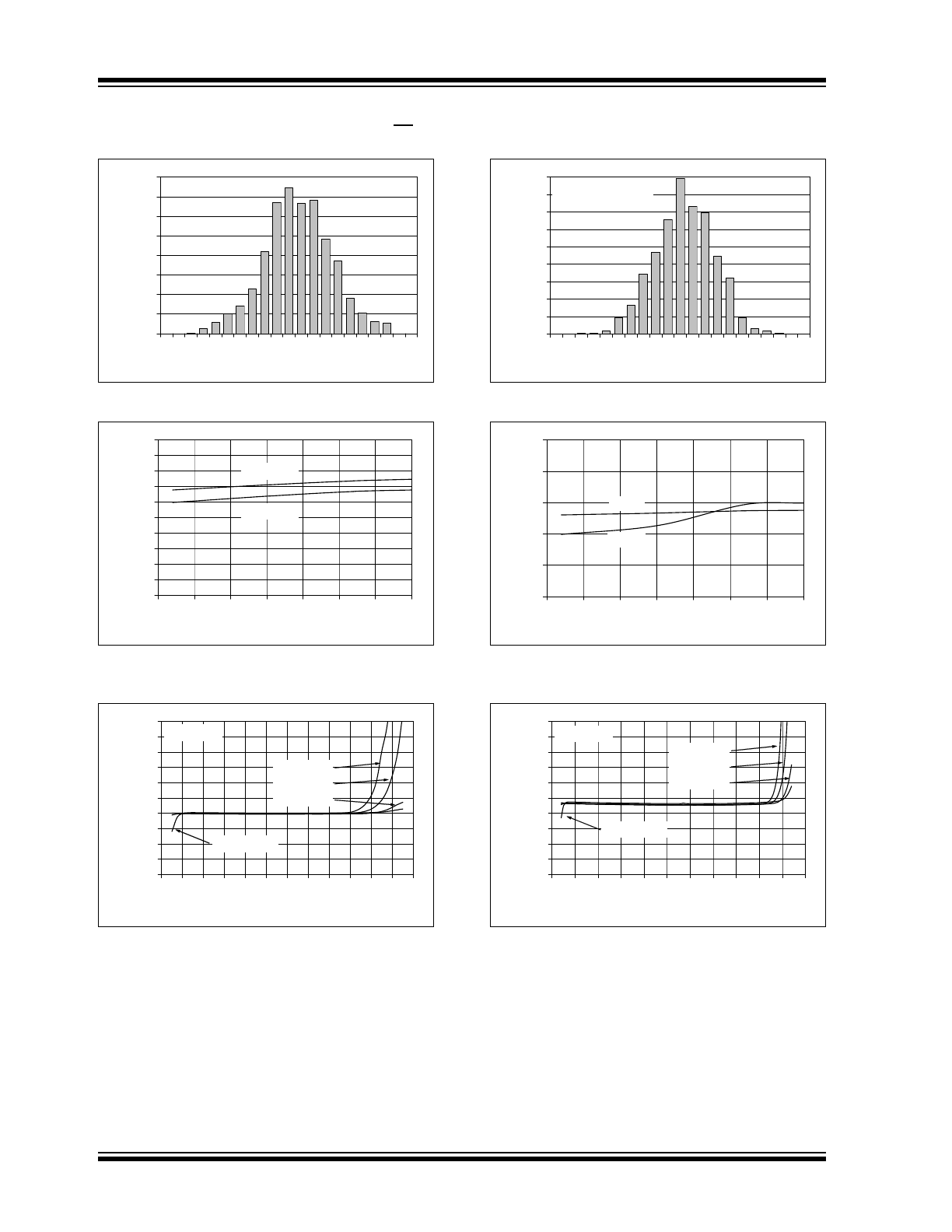
FIGURE 2-7:
Input Offset Voltage.
FIGURE 2-8:
Input Offset Voltage vs.
Temperature.
FIGURE 2-9:
Input Offset Voltage vs.
Common Mode Input Voltage with V
DD
= 2.7V.
FIGURE 2-10:
Input Offset Voltage Drift.
FIGURE 2-11:
CMRR, PSRR vs.
Temperature.
FIGURE 2-12:
Input Offset Voltage vs.
Common Mode Input Voltage with V
DD
= 5.5V.
0%
2%
4%
6%
8%
10%
12%
14%
16%
-2.0 -1.6 -1.2 -0.8 -0.4 0.0 0.4 0.8 1.2 1.6 2.0
Input Offset Voltage (mV)
P
e
rcentage of
Occurrences
1200 Samples
-0.5
-0.4
-0.3
-0.2
-0.1
0.0
0.1
0.2
0.3
0.4
0.5
-50
-25
0
25
50
75
100
125
Ambient Temperature (°C)
Input
Off
set Voltag
e (
m
V)
V
DD
= 2.7V
V
DD
= 5.5V
-200
-100
0
100
200
300
400
500
600
700
800
-0
.4
-0
.2
0.
0
0.
2
0.
4
0.
6
0.
8
1.
0
1.
2
1.
4
1.
6
1.
8
2.
0
Common Mode Input Voltage (V)
Input
O
ffs
et
Vol
ta
g
e (
µ
V)
V
DD
= 2.7V
T
A
= –40°C
T
A
= +25°C
T
A
= +85°C
T
A
= +125°C
0%
2%
4%
6%
8%
10%
12%
14%
16%
18%
-10 -8
-6
-4
-2
0
2
4
6
8
10
Input Offset Voltage Drift (µV/°C)
Percent
age of Occurrences
1200 Samples
T
A
= –40 to +125°C
75
80
85
90
95
100
-50
-25
0
25
50
75
100
125
Ambient Temperature (°C)
CM
R
R
, PSRR (
d
B)
PSRR
CMRR
-200
-100
0
100
200
300
400
500
600
700
800
-0
.5
0.
0
0.
5
1.
0
1.
5
2.
0
2.
5
3.
0
3.
5
4.
0
4.
5
5.
0
Common Mode Input Voltage (V)
Input
O
ffs
et
Vol
ta
g
e (
µ
V)
V
DD
= 5.5V
T
A
= –40°C
T
A
= +25°C
T
A
= +85°C
T
A
= +125°C
© 2007 Microchip Technology Inc.
DS21314G-page 7
MCP601/1R/2/3/4
Note: Unless otherwise indicated, T
A
= +25°C, V
DD
= +2.7V to +5.5V, V
SS
= GND, V
CM
= V
DD
/2, V
OUT
≈ V
DD
/2,
V
L
= V
DD
/2, R
L
= 100 k
Ω to V
L
, C
L
= 50 pF and CS is tied low.
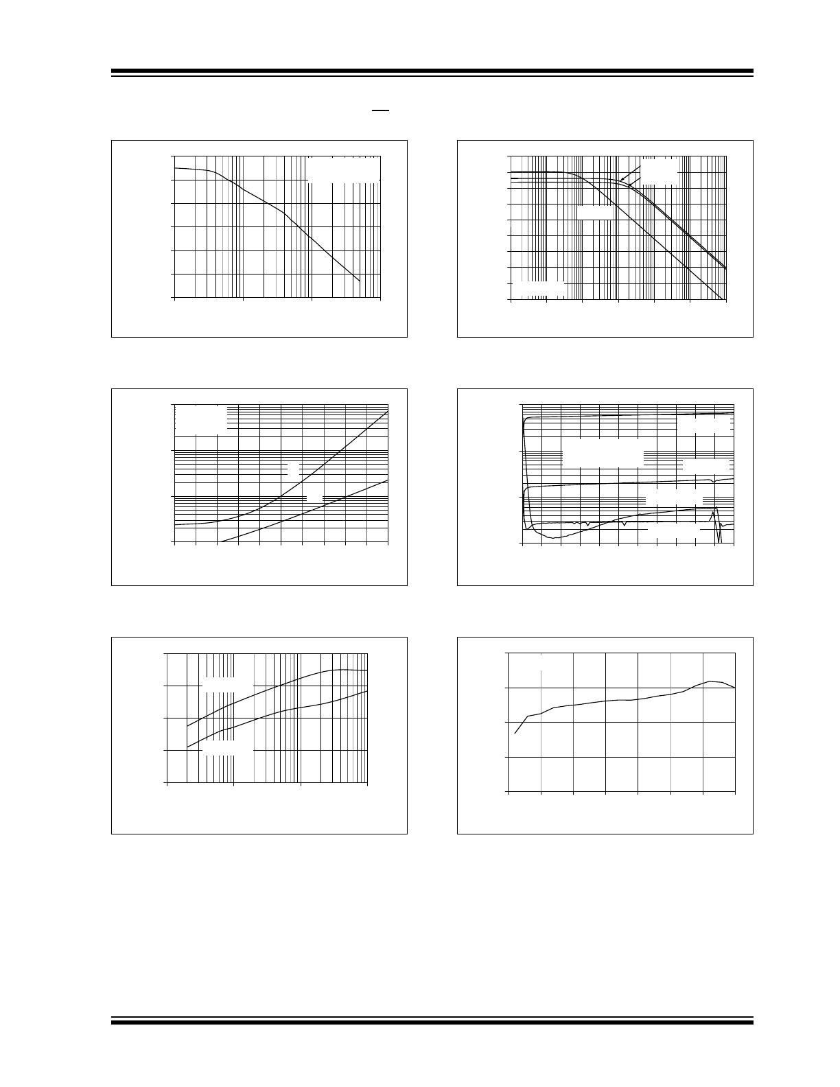
FIGURE 2-13:
Channel-to-Channel
Separation vs. Frequency.
FIGURE 2-14:
Input Bias Current, Input
Offset Current vs. Ambient Temperature.
FIGURE 2-15:
DC Open-Loop Gain vs.
Load Resistance.
FIGURE 2-16:
CMRR, PSRR vs.
Frequency.
FIGURE 2-17:
Input Bias Current, Input
Offset Current vs. Common Mode Input Voltage.
FIGURE 2-18:
DC Open-Loop Gain vs.
Supply Voltage.
90
100
110
120
130
140
150
1.E+03
1.E+04
1.E+05
1.E+06
Frequency (Hz)
Channel-
to-
C
hannel
S
e
paration (
d
B)
No Load
Input Referred
1k
10k
100k
1M
1
10
100
1000
25 35 45 55 65 75 85 95 105 115 125
Ambient Temperature (°C)
Input Bias and Off
set
Currents (pA)
I
B
V
DD
= 5.5V
V
CM
= 4.3V
I
OS
80
90
100
110
120
1.E+02
1.E+03
1.E+04
1.E+05
Load Resistance (Ω)
D
C
Open-Loop Gain (
d
B
)
V
DD
= 2.7V
V
DD
= 5.5V
100
1k
10k
100k
10
20
30
40
50
60
70
80
90
100
1.E+00 1.E+01 1.E+02 1.E+03 1.E+04 1.E+05 1.E+06
Frequency (Hz)
CMRR, PSRR (
d
B)
CMRR
V
DD
= 5.0V
1
100
10k
1M
PSRR+
PSRR–
10
1k
100k
1
10
100
1000
0.0 0.5 1.0 1.5 2.0 2.5 3.0 3.5 4.0 4.5 5.0 5.5
Common Mode Input Voltage (V)
Input Bias and Off
set
Currents (pA)
I
B
, +85°C
V
DD
= 5.5V
max. V
CMR
≥ 4.3V
I
B
, +125°C
I
OS
, +85°C
I
OS
, +125°C
80
90
100
110
120
2.0
2.5
3.0
3.5
4.0
4.5
5.0
5.5
Power Supply Voltage (V)
DC
Open-Loop Gain (dB)
R
L
= 25 kΩ
MCP601/1R/2/3/4
DS21314G-page 8
© 2007 Microchip Technology Inc.
Note: Unless otherwise indicated, T
A
= +25°C, V
DD
= +2.7V to +5.5V, V
SS
= GND, V
CM
= V
DD
/2, V
OUT
≈ V
DD
/2,
V
L
= V
DD
/2, R
L
= 100 k
Ω to V
L
, C
L
= 50 pF and CS is tied low.
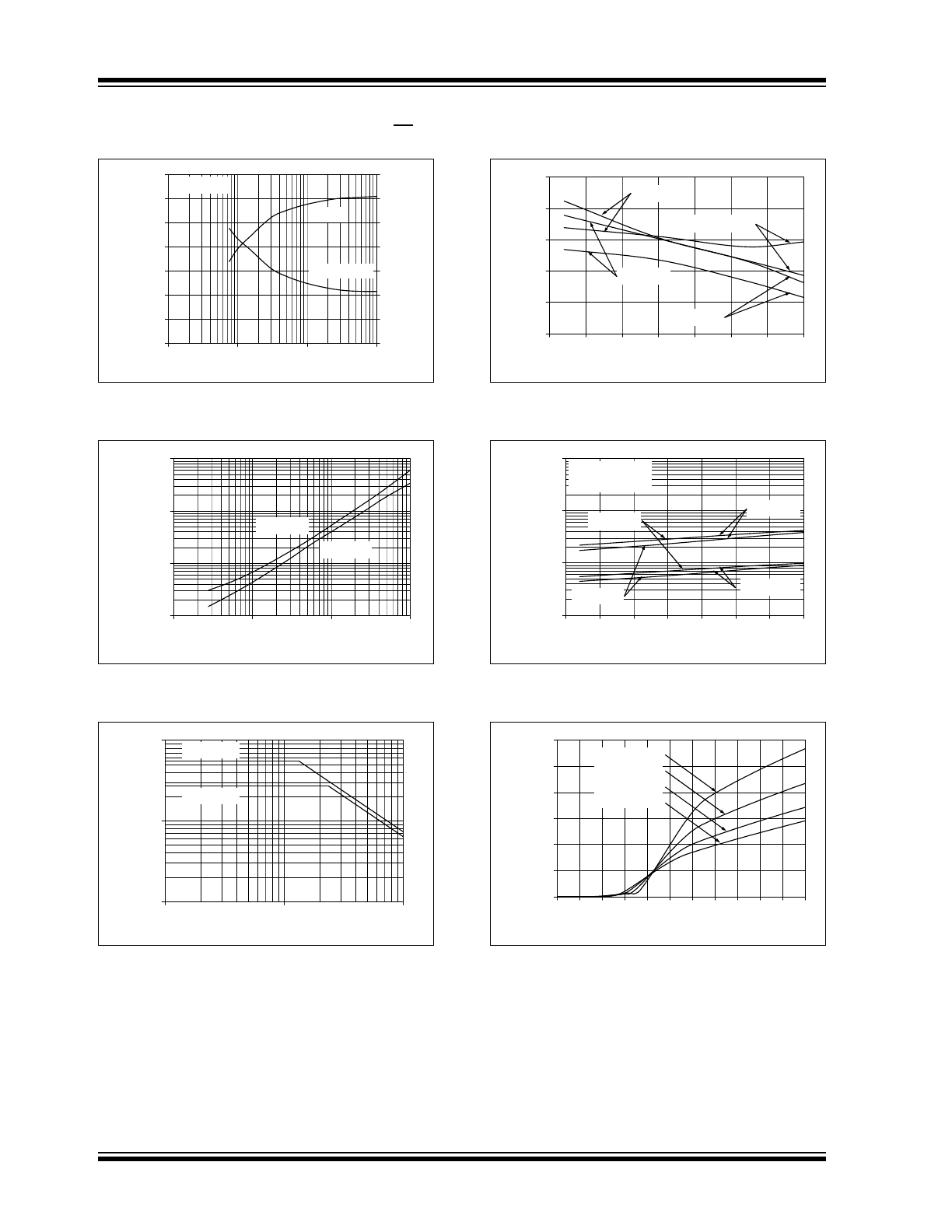
FIGURE 2-19:
Gain Bandwidth Product,
Phase Margin vs. Load Resistance.
FIGURE 2-20:
Output Voltage Headroom
vs. Output Current.
FIGURE 2-21:
Maximum Output Voltage
Swing vs. Frequency.
FIGURE 2-22:
DC Open-Loop Gain vs.
Temperature.
FIGURE 2-23:
Output Voltage Headroom
vs. Temperature.
FIGURE 2-24:
Output Short-Circuit Current
vs. Supply Voltage.
0.0
0.5
1.0
1.5
2.0
2.5
3.0
3.5
1.E+02
1.E+03
1.E+04
1.E+05
Load Resistance (Ω)
G
a
in Bandwidth Product
(M
Hz)
30
40
50
60
70
80
90
100
P
h
as
e Ma
rgin, G = +1 (°)
100
10k
1k
100k
V
DD
= 5.0V
GBWP
PM, G = +1
1
10
100
1,000
0.01
0.1
1
10
Output Current Magnitude (mA)
Out
put Headroom (
m
V
);
V
DD
– V
OH
and V
OL
– V
SS
V
DD
– V
OH
V
OL
– V
SS
0.1
1
10
1.E+04
1.E+05
1.E+06
Frequency (Hz)
Max
imum Output Voltag
e
Swing (V
P-
P
)
10k
100k
1M
V
DD
= 5.5V
V
DD
= 2.7V
80
90
100
110
120
130
-50
-25
0
25
50
75
100
125
Ambient Temperature (°C)
DC Open-
Loop Gain (
d
B)
V
DD
= 5.5V
V
DD
= 2.7V
R
L
= 25 kΩ
R
L
= 5 kΩ
1
10
100
1000
-50
-25
0
25
50
75
100
125
Ambient Temperature (°C)
Output
Headroo
m
(
m
V
);
V
DD
– V
OH
and V
OL
– V
SS
V
DD
– V
OH
R
L
= 25 kΩ
V
DD
= 5.5V
R
L
tied to V
DD
/2
V
OL
– V
SS
R
L
= 5 kΩ
0
5
10
15
20
25
30
0.0 0.5 1.0 1.5 2.0 2.5 3.0 3.5 4.0 4.5 5.0 5.5
Supply Voltage (V)
Out
put Short Circuit Current
M
agnit
ude (
m
A
)
T
A
= –40°C
T
A
= +25°C
T
A
= +85°C
T
A
= +125°C
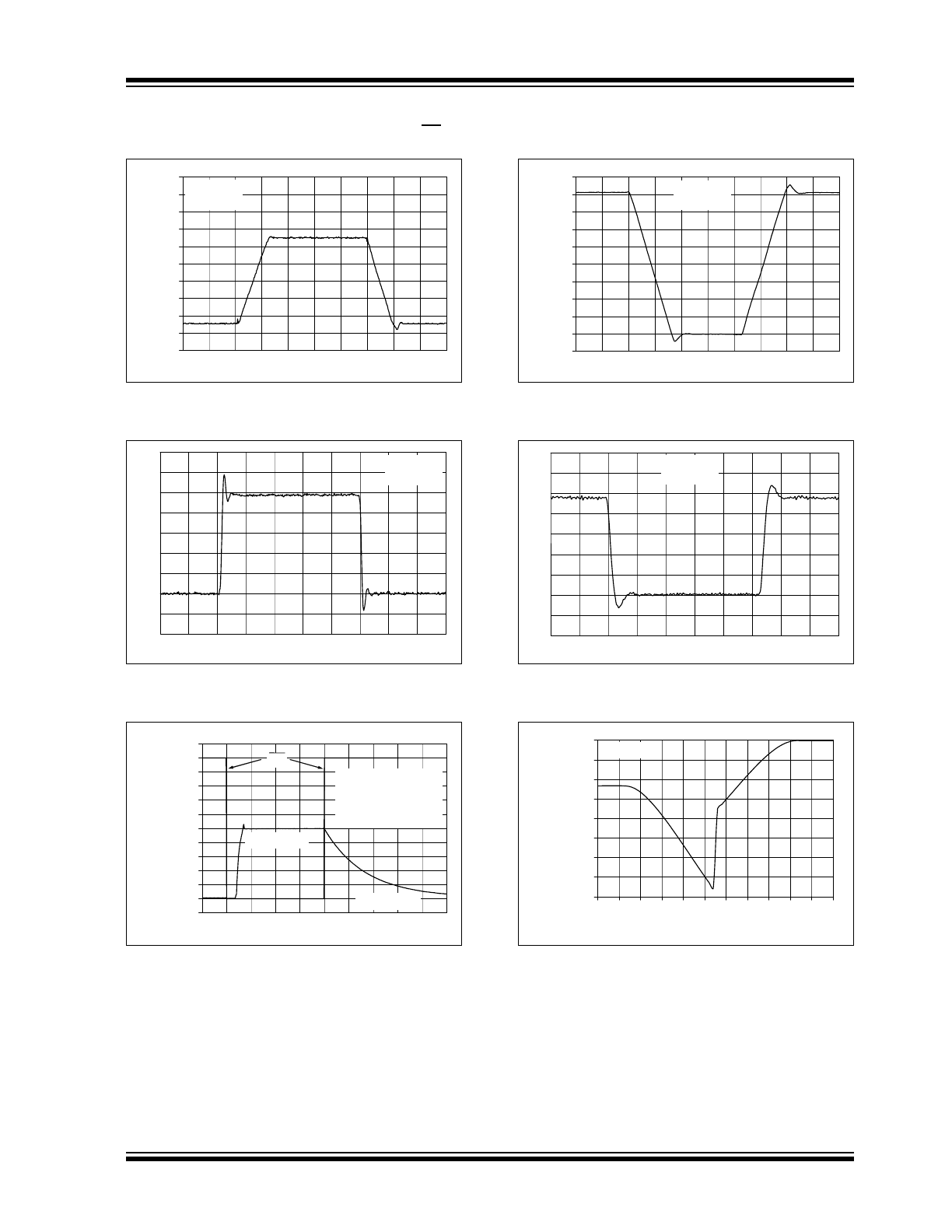
© 2007 Microchip Technology Inc.
DS21314G-page 9
MCP601/1R/2/3/4
Note: Unless otherwise indicated, T
A
= +25°C, V
DD
= +2.7V to +5.5V, V
SS
= GND, V
CM
= V
DD
/2, V
OUT
≈ V
DD
/2,
V
L
= V
DD
/2, R
L
= 100 k
Ω to V
L
, C
L
= 50 pF and CS is tied low.
FIGURE 2-25:
Large Signal Non-Inverting
Pulse Response.
FIGURE 2-26:
Small Signal Non-Inverting
Pulse Response.
FIGURE 2-27:
Chip Select Timing
(MCP603).
FIGURE 2-28:
Large Signal Inverting Pulse
Response.
FIGURE 2-29:
Small Signal Inverting Pulse
Response.
FIGURE 2-30:
Quiescent Current Through
V
SS
vs. Chip Select Voltage (MCP603).
0.0
0.5
1.0
1.5
2.0
2.5
3.0
3.5
4.0
4.5
5.0
Time (1 µs/div)
Output V
o
lta
g
e (V)
V
DD
= 5.0V
G = +1
Time (1 µs/div)
Output V
o
lta
g
e (20
mV/div
)
V
DD
= 5.0V
G = +1
-0.5
0.0
0.5
1.0
1.5
2.0
2.5
3.0
3.5
4.0
4.5
5.0
5.5
Time (5 µs/div)
Out
put Voltage,
Chip S
e
le
ct Voltage
(V
)
V
DD
= 5.0V
G = +1
V
IN
= 2.5V
R
L
= 100 kΩ to GND
CS
V
OUT
Active
V
OUT
High-Z
0.0
0.5
1.0
1.5
2.0
2.5
3.0
3.5
4.0
4.5
5.0
Time (1 µs/div)
O
u
tput
V
o
lt
age (V)
V
DD
= 5.0V
G = –1
Time (1 µs/div)
Output V
o
lta
g
e (20
mV/div
)
V
DD
= 5.0V
G = –1
-800
-700
-600
-500
-400
-300
-200
-100
0
0.0 0.5 1.0 1.5 2.0 2.5 3.0 3.5 4.0 4.5 5.0 5.5
Chip Select Voltage (V)
Q
u
ie
sc
ent
Cur
re
nt
through V
SS
(µA)
V
DD
= 5.5V
MCP601/1R/2/3/4
DS21314G-page 10
© 2007 Microchip Technology Inc.
Note: Unless otherwise indicated, T
A
= +25°C, V
DD
= +2.7V to +5.5V, V
SS
= GND, V
CM
= V
DD
/2, V
OUT
≈ V
DD
/2,
V
L
= V
DD
/2, R
L
= 100 k
Ω to V
L
, C
L
= 50 pF and CS is tied low.
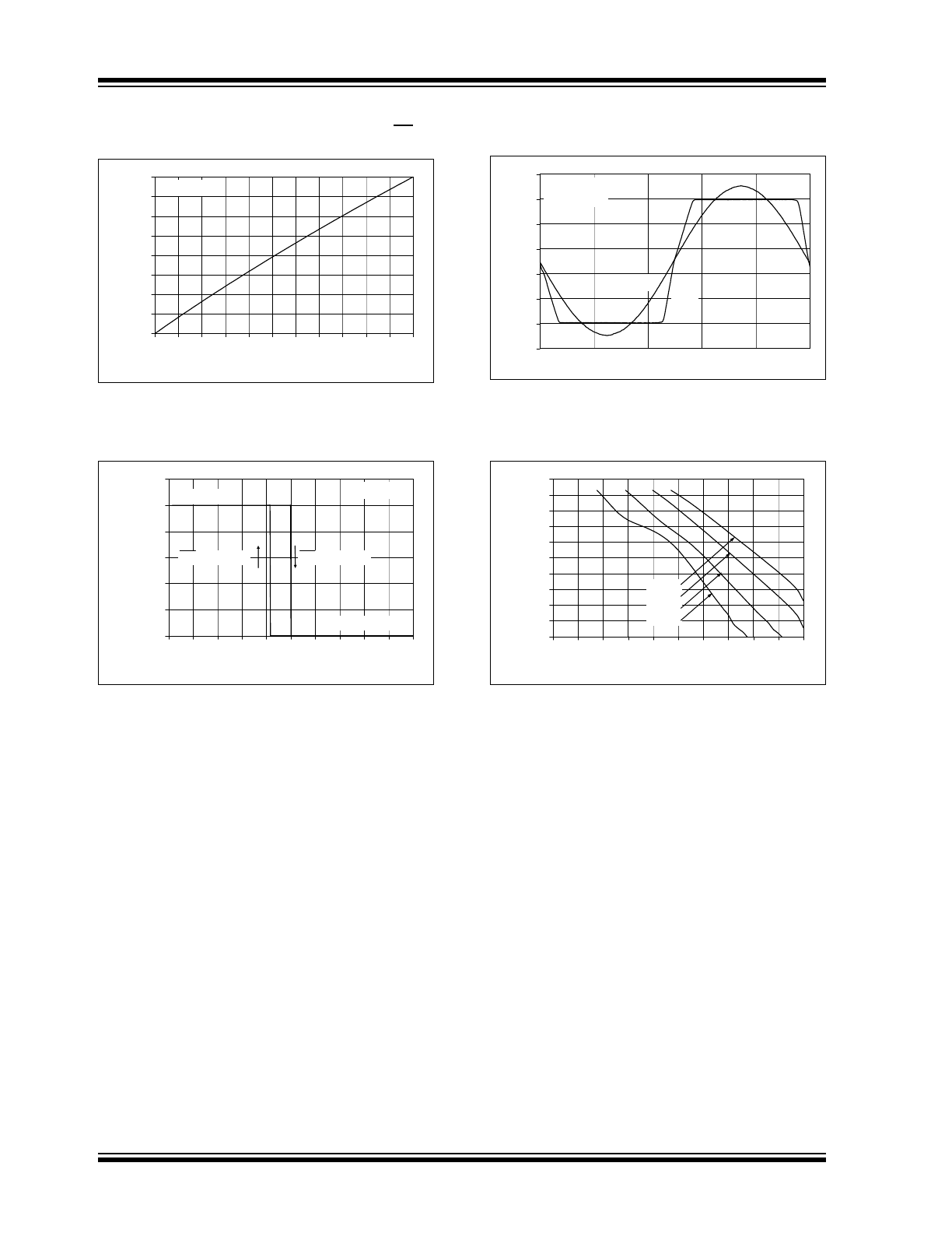
FIGURE 2-31:
Chip Select Pin Input
Current vs. Chip Select Voltage.
FIGURE 2-32:
Hysteresis of Chip Select’s
Internal Switch.
FIGURE 2-33:
The MCP601/1R/2/3/4
family of op amps shows no phase reversal
under input overdrive.
FIGURE 2-34:
Measured Input Current vs.
Input Voltage (below V
SS
).
0.0
0.1
0.2
0.3
0.4
0.5
0.6
0.7
0.8
0.0 0.5 1.0 1.5 2.0 2.5 3.0 3.5 4.0 4.5 5.0 5.5
Chip Select Voltage (V)
Chip Se
lec
t P
in
Cu
rr
en
t (µA)
V
DD
= 5.5V
0.0
0.5
1.0
1.5
2.0
2.5
3.0
0.0 0.5 1.0 1.5 2.0 2.5 3.0 3.5 4.0 4.5 5.0
Chip Select Voltage (V)
Interna
l Chip Se
lec
t S
w
itc
h
Outp
ut V
o
lta
g
e (V)
V
DD
= 5.0V
Amplifier Hi-Z
Amplifier On
CS Hi to Low
CS Low to Hi
-1
0
1
2
3
4
5
6
Time (5 µs/div)
Input an
d Out
put Voltages (V)
V
DD
= +5.0V
G = +2
V
IN
V
OUT
1.E-12
1.E-11
1.E-10
1.E-09
1.E-08
1.E-07
1.E-06
1.E-05
1.E-04
1.E-03
1.E-02
-1.0 -0.9 -0.8 -0.7 -0.6 -0.5 -0.4 -0.3 -0.2 -0.1 0.0
Input Voltage (V)
Input Current M
agnit
ude (
A
)
+125°C
+85°C
+25°C
-40°C
10m
1m
100µ
10µ
1µ
100n
10n
1n
100p
10p
1p