
© 2008 Microchip Technology Inc.
DS21295D-page 1
MCP3004/3008
Features
• 10-bit resolution
• ± 1 LSB max DNL
• ± 1 LSB max INL
• 4 (MCP3004) or 8 (MCP3008) input channels
• Analog inputs programmable as single-ended or
pseudo-differential pairs
• On-chip sample and hold
• SPI serial interface (modes 0,0 and 1,1)
• Single supply operation: 2.7V - 5.5V
• 200 ksps max. sampling rate at V
DD
= 5V
• 75 ksps max. sampling rate at V
DD
= 2.7V
• Low power CMOS technology
• 5 nA typical standby current, 2 µA max.
• 500 µA max. active current at 5V
• Industrial temp range: -40°C to +85°C
• Available in PDIP, SOIC and TSSOP packages
Applications
• Sensor Interface
• Process Control
• Data Acquisition
• Battery Operated Systems
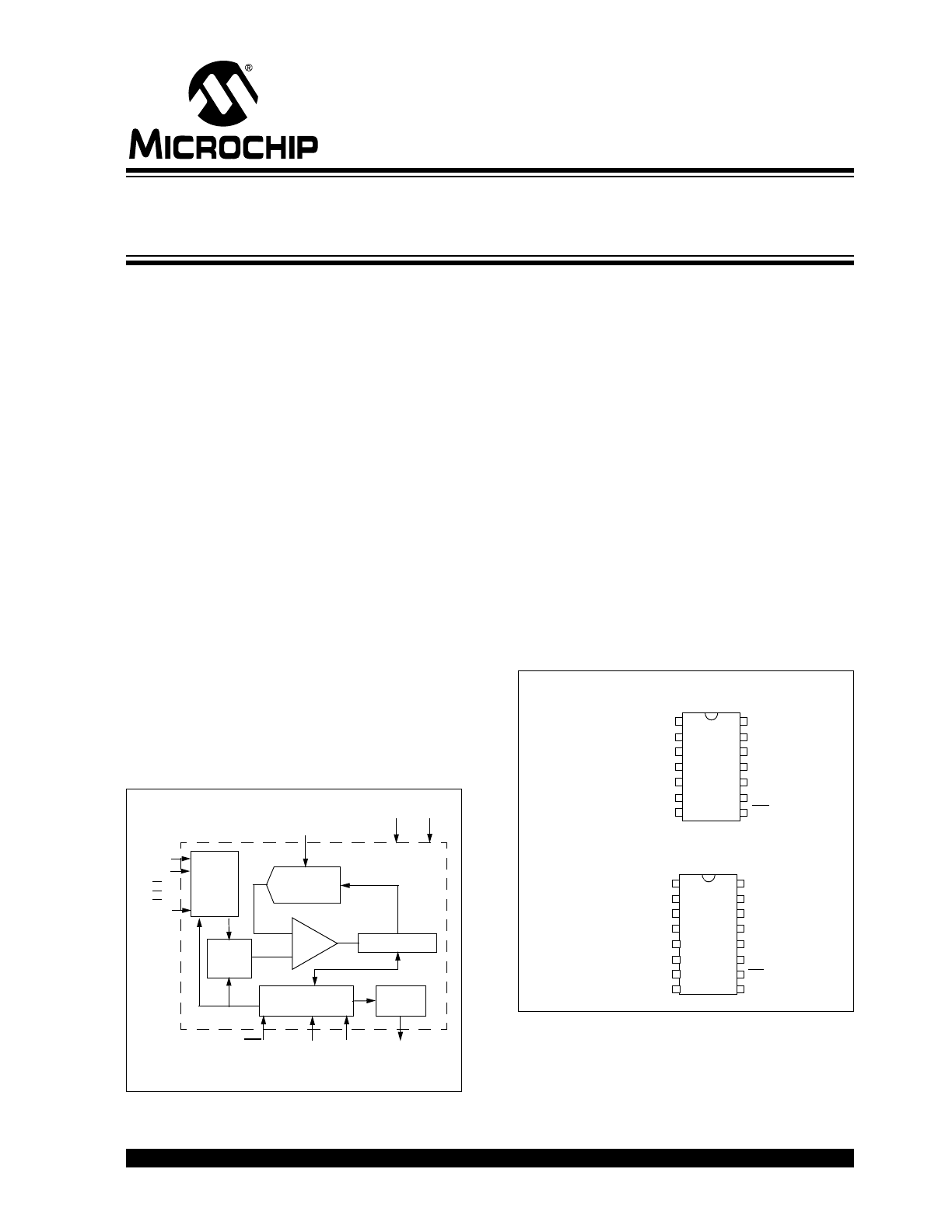
Functional Block Diagram
Description
The Microchip Technology Inc. MCP3004/3008
devices are successive approximation 10-bit Analog-
to-Digital (A/D) converters with on-board sample and
hold circuitry. The MCP3004 is programmable to
provide two pseudo-differential input pairs or four
single-ended inputs. The MCP3008 is programmable
to provide four pseudo-differential input pairs or eight
single-ended inputs. Differential Nonlinearity (DNL)
and Integral Nonlinearity (INL) are specified at ±1 LSB.
Communication with the devices is accomplished using
a simple serial interface compatible with the SPI
protocol. The devices are capable of conversion rates
of up to 200 ksps. The MCP3004/3008 devices operate
over a broad voltage range (2.7V - 5.5V). Low-current
design permits operation with typical standby currents
of only 5 nA and typical active currents of 320 µA. The
MCP3004 is offered in 14-pin PDIP, 150 mil SOIC and
TSSOP packages, while the MCP3008 is offered in 16-
pin PDIP and SOIC packages.
Package Types
Comparator
Sample
and
Hold
10-Bit SAR
DAC
Control Logic
CS/SHDN
V
REF
V
SS
V
DD
CLK
D
OUT
Shift
Register
CH0
Channel
Max
Input
CH1
CH7*
* Note: Channels 4-7 are available on MCP3008 Only
D
IN
V
DD
CLK
D
OUT
MCP3
004
1
2
3
4
14
13
12
11
10
9
8
5
6
7
V
REF
D
IN
CH0
CH1
CH2
CH3
CS/SHDN
DGND
AGND
NC
V
DD
CLK
D
OUT
MC
P3008
1
2
3
4
16
15
14
13
12
11
10
9
5
6
7
8
V
REF
D
IN
CS/SHDN
DGND
CH0
CH1
CH2
CH3
CH4
CH5
CH6
CH7
NC
AGND
PDIP, SOIC, TSSOP
PDIP, SOIC
2.7V 4-Channel/8-Channel 10-Bit A/D Converters
with SPI Serial Interface

MCP3004/3008
DS21295D-page 2
© 2008 Microchip Technology Inc.
NOTES:
© 2008 Microchip Technology Inc.
DS21295D-page 3
MCP3004/3008
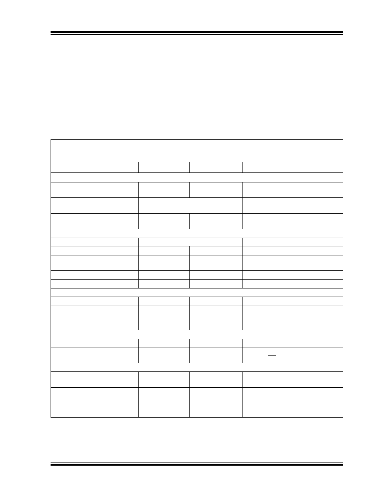
1.0
ELECTRICAL
CHARACTERISTICS
Absolute Maximum Ratings †
V
DD
..................................................................................7.0V
All Inputs and Outputs w.r.t. V
SS
............– 0.6V to V
DD
+ 0.6V
Storage Temperature ................................... –65°C to +150°C
Ambient temperature with power applied.......–65°C to +150°C
Soldering temperature of leads (10 seconds) ............. +300°C
ESD Protection On All Pins (HBM)
...................................≥ 4 kV
† Notice:
Stresses above those listed under “Absolute
Maximum Ratings” may cause permanent damage to the
device. This is a stress rating only and functional operation of
the device at those or any other conditions above those
indicated in the operational listings of this specification is not
implied. Exposure to maximum rating conditions for extended
periods may affect device reliability.
ELECTRICAL SPECIFICATIONS
Electrical Characteristics:
Unless otherwise noted, all parameters apply at V
DD
= 5V, V
REF
= 5V,
T
A
= -40°C to +85°C, f
SAMPLE
= 200 ksps and f
CLK
= 18*f
SAMPLE
. Unless otherwise noted, typical values apply for
V
DD
= 5V, T
A
= +25°C.
Parameter
Sym
Min
Typ
Max
Units
Conditions
Conversion Rate
Conversion Time
t
CONV
—
—
10
clock
cycles
Analog Input Sample Time
t
SAMPLE
1.5
clock
cycles
Throughput Rate
f
SAMPLE
—
—
200
75
ksps
ksps
V
DD
= V
REF
= 5V
V
DD
= V
REF
= 2.7V
DC Accuracy
Resolution
10
bits
Integral Nonlinearity
INL
—
±0.5
±1
LSB
Differential Nonlinearity
DNL
—
±0.25
±1
LSB
No missing codes over
temperature
Offset Error
—
—
±1.5
LSB
Gain Error
—
—
±1.0
LSB
Dynamic Performance
Total Harmonic Distortion
—
-76
dB
V
IN
= 0.1V to 4.9V@1 kHz
Signal-to-Noise and Distortion
(SINAD)
—
61
dB
V
IN
= 0.1V to 4.9V@1 kHz
Spurious Free Dynamic Range
—
78
dB
V
IN
= 0.1V to 4.9V@1 kHz
Reference Input
Voltage Range
0.25
—
V
DD
V
Note 2
Current Drain
—
100
0.001
150
3
µA
µA
CS = V
DD
= 5V
Analog Inputs
Input Voltage Range for CH0 or
CH1 in Single-Ended Mode
V
SS
—
V
REF
V
Input Voltage Range for IN+ in
pseudo-differential mode
IN-
—
V
REF
+IN-
Input Voltage Range for IN- in
pseudo-differential mode
V
SS
-100
—
V
SS
+100
mV
Note 1:
This parameter is established by characterization and not 100% tested.
2:
See graphs that relate linearity performance to V
REF
levels.
3:
Because the sample cap will eventually lose charge, effective clock rates below 10 kHz can affect linearity
performance, especially at elevated temperatures. See Section 6.2 “Maintaining Minimum Clock
Speed”
, “Maintaining Minimum Clock Speed”, for more information.
MCP3004/3008
DS21295D-page 4
© 2008 Microchip Technology Inc.
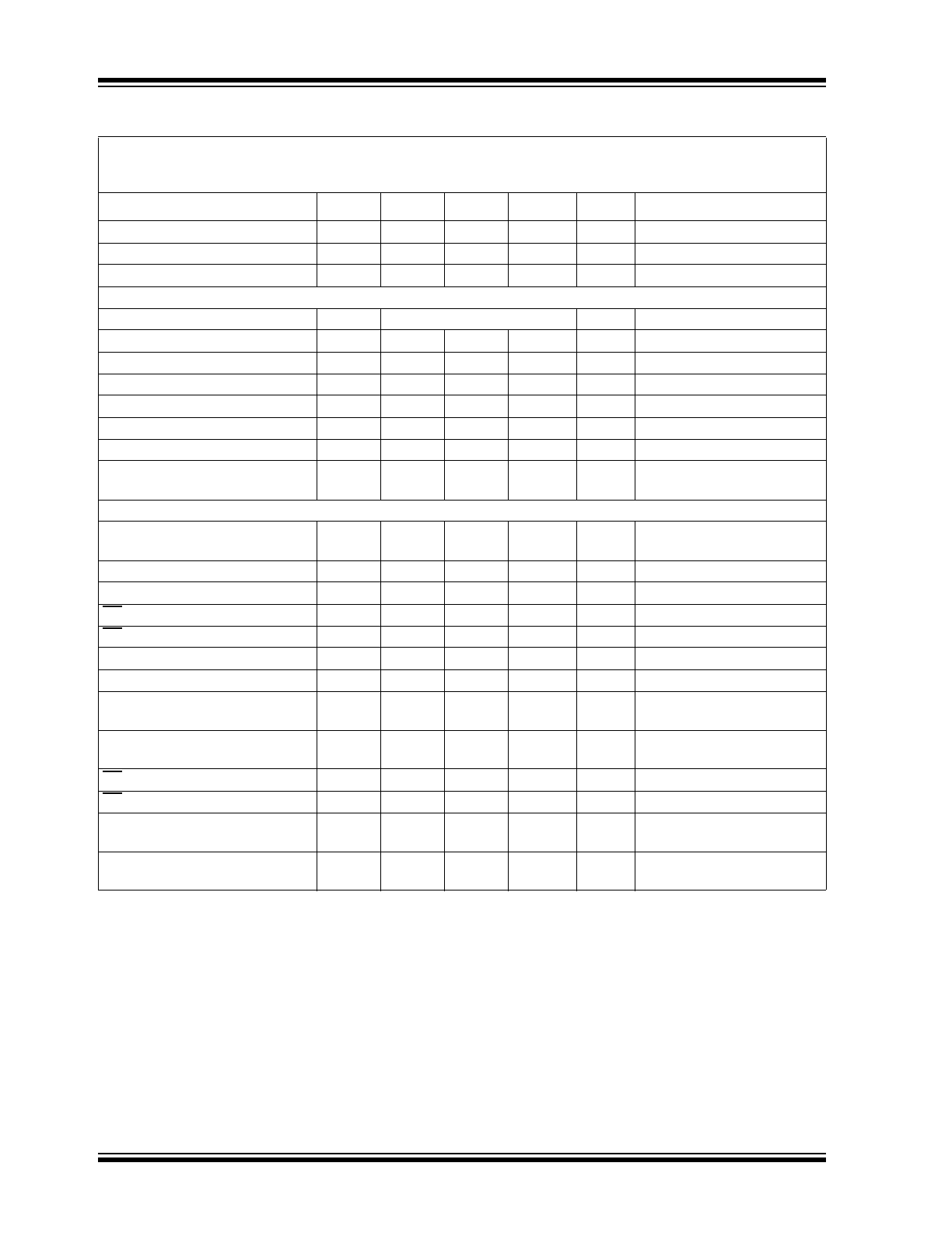
Leakage Current
—
0.001
±1
µA
Switch Resistance
—
1000
—
Ω
See
Figure 4-1
Sample Capacitor
—
20
—
pF
See
Figure 4-1
Digital Input/Output
Data Coding Format
Straight Binary
High Level Input Voltage
V
IH
0.7 V
DD
—
—
V
Low Level Input Voltage
V
IL
—
0.3 V
DD
V
High Level Output Voltage
V
OH
4.1
—
—
V
I
OH
= -1 mA, V
DD
= 4.5V
Low Level Output Voltage
V
OL
—
—
0.4
V
I
OL
= 1 mA, V
DD
= 4.5V
Input Leakage Current
I
LI
-10
—
10
µA
V
IN
= V
SS
or V
DD
Output Leakage Current
I
LO
-10
—
10
µA
V
OUT
= V
SS
or V
DD
Pin Capacitance
(All Inputs/Outputs)
C
IN
,
C
OUT
—
—
10
pF
V
DD
= 5.0V (Note 1)
T
A
= 25°C, f = 1 MHz
Timing Parameters
Clock Frequency
f
CLK
—
—
3.6
1.35
MHz
MHz
V
DD
= 5V (Note 3)
V
DD
= 2.7V (Note 3)
Clock High Time
t
HI
125
—
—
ns
Clock Low Time
t
LO
125
—
—
ns
CS Fall To First Rising CLK Edge
t
SUCS
100
—
—
ns
CS Fall To Falling CLK Edge
t
CSD
—
—
0
ns
Data Input Setup Time
t
SU
50
—
—
ns
Data Input Hold Time
t
HD
50
—
—
ns
CLK Fall To Output Data Valid
t
DO
—
—
125
200
ns
ns
V
DD
= 5V, See
Figure 1-2
V
DD
= 2.7V, See
Figure 1-2
CLK Fall To Output Enable
t
EN
—
—
125
200
ns
ns
V
DD
= 5V, See
Figure 1-2
V
DD
= 2.7V, See
Figure 1-2
CS Rise To Output Disable
t
DIS
—
—
100
ns
See Test Circuits,
Figure 1-2
CS Disable Time
t
CSH
270
—
—
ns
D
OUT
Rise Time
t
R
—
—
100
ns
See Test Circuits,
Figure 1-2
(Note 1)
D
OUT
Fall Time
t
F
—
—
100
ns
See Test Circuits,
Figure 1-2
(Note 1)
ELECTRICAL SPECIFICATIONS (CONTINUED)
Electrical Characteristics:
Unless otherwise noted, all parameters apply at V
DD
= 5V, V
REF
= 5V,
T
A
= -40°C to +85°C, f
SAMPLE
= 200 ksps and f
CLK
= 18*f
SAMPLE
. Unless otherwise noted, typical values apply for
V
DD
= 5V, T
A
= +25°C.
Parameter
Sym
Min
Typ
Max
Units
Conditions
Note 1:
This parameter is established by characterization and not 100% tested.
2:
See graphs that relate linearity performance to V
REF
levels.
3:
Because the sample cap will eventually lose charge, effective clock rates below 10 kHz can affect linearity
performance, especially at elevated temperatures. See Section 6.2 “Maintaining Minimum Clock
Speed”
, “Maintaining Minimum Clock Speed”, for more information.
© 2008 Microchip Technology Inc.
DS21295D-page 5
MCP3004/3008
TEMPERATURE CHARACTERISTICS
FIGURE 1-1:
Serial Interface Timing.
Power Requirements
Operating Voltage
V
DD
2.7
—
5.5
V
Operating Current
I
DD
—
425
225
550
µA
V
DD
= V
REF
= 5V,
D
OUT
unloaded
V
DD
= V
REF
= 2.7V,
D
OUT
unloaded
Standby Current
I
DDS
—
0.005
2
µA
CS = V
DD
= 5.0V
Electrical Specifications:
Unless otherwise indicated, V
DD
= +2.7V to +5.5V, V
SS
= GND.
Parameters
Sym
Min
Typ
Max
Units
Conditions
Temperature Ranges
Specified Temperature Range
T
A
-40
—
+85
°C
Operating Temperature Range
T
A
-40
—
+85
°C
Storage Temperature Range
T
A
-65
—
+150
°C
Thermal Package Resistances
Thermal Resistance, 14L-PDIP
θ
JA
—
70
—
°C/W
Thermal Resistance, 14L-SOIC
θ
JA
—
108
—
°C/W
Thermal Resistance, 14L-TSSOP
θ
JA
—
100
—
°C/W
Thermal Resistance, 16L-PDIP
θ
JA
—
70
—
°C/W
Thermal Resistance, 16L-SOIC
θ
JA
—
90
—
°C/W
ELECTRICAL SPECIFICATIONS (CONTINUED)
Electrical Characteristics:
Unless otherwise noted, all parameters apply at V
DD
= 5V, V
REF
= 5V,
T
A
= -40°C to +85°C, f
SAMPLE
= 200 ksps and f
CLK
= 18*f
SAMPLE
. Unless otherwise noted, typical values apply for
V
DD
= 5V, T
A
= +25°C.
Parameter
Sym
Min
Typ
Max
Units
Conditions
Note 1:
This parameter is established by characterization and not 100% tested.
2:
See graphs that relate linearity performance to V
REF
levels.
3:
Because the sample cap will eventually lose charge, effective clock rates below 10 kHz can affect linearity
performance, especially at elevated temperatures. See Section 6.2 “Maintaining Minimum Clock
Speed”
, “Maintaining Minimum Clock Speed”, for more information.
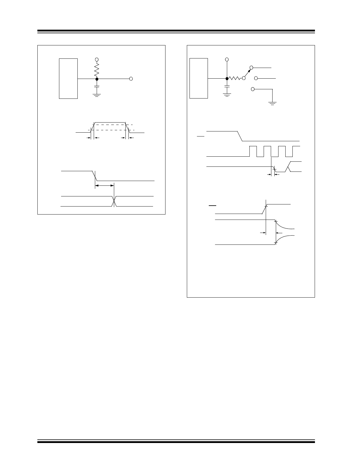
CS
CLK
D
IN
MSB IN
T
SU
T
HD
T
SUCS
T
CSH
T
HI
T
LO
D
OUT
T
EN
T
DO
T
R
T
F
LSB
MSB OUT
T
DIS
NULL BIT
MCP3004/3008
DS21295D-page 6
© 2008 Microchip Technology Inc.
FIGURE 1-2:
Load Circuit for t
R
, t
F
, t
DO
.
FIGURE 1-3:
Load circuit for t
DIS
and t
EN
.
Test Point
1.4V
D
OUT
3 k
Ω
C
L
= 100 pF
D
OUT
tR
Voltage Waveforms for t
R
, t
F
CLK
D
OUT
t
DO
Voltage Waveforms for t
DO
tF
V
OH
V
OL
90%
10%
*
Waveform 1 is for an output with internal
conditions such that the output is high,
unless disabled by the output control.
†
Waveform 2 is for an output with internal
conditions such that the output is low,
unless disabled by the output control.
Test Point
D
OUT
3 k
Ω
100 pF
t
DIS
Waveform 2
t
DIS
Waveform 1
CS
CLK
D
OUT
t
EN
1
2
B9
Voltage Waveforms for tEN
t
EN
Waveform
V
DD
V
DD
/2
V
SS
3
4
Voltage Waveforms for t
DIS
D
OUT
D
OUT
CS
V
IH
T
DIS
Waveform 1*
Waveform 2†
© 2008 Microchip Technology Inc.
DS21295D-page 7
MCP3004/3008
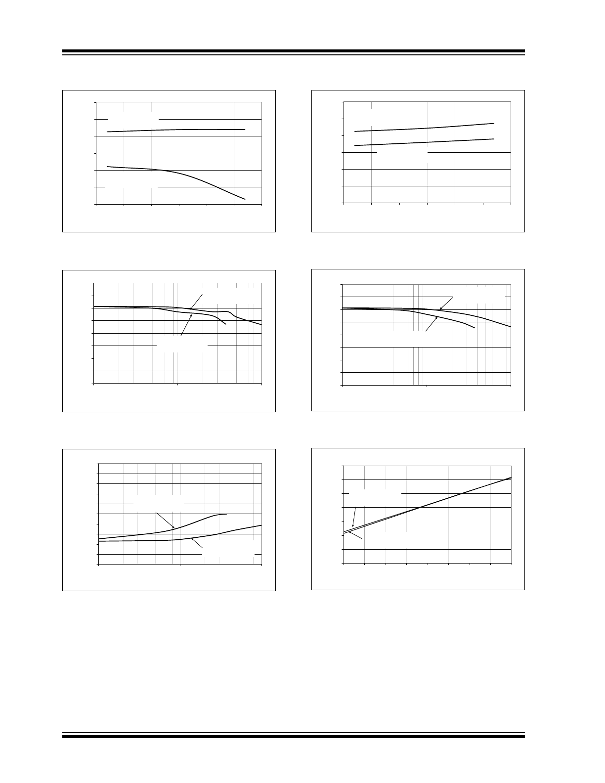
2.0
TYPICAL PERFORMANCE CHARACTERISTICS
Note:
Unless otherwise indicated, V
DD
= V
REF
= 5V, f
CLK
= 18* f
SAMPLE
, T
A
= +25°C.
FIGURE 2-1:
Integral Nonlinearity (INL)
vs. Sample Rate.
FIGURE 2-2:
Integral Nonlinearity (INL)
vs. V
REF
.
FIGURE 2-3:
Integral Nonlinearity (INL)
vs. Code (Representative Part).
FIGURE 2-4:
Integral Nonlinearity (INL)
vs. Sample Rate (V
DD
= 2.7V).
FIGURE 2-5:
Integral Nonlinearity (INL)
vs. V
REF
(V
DD
= 2.7V).
FIGURE 2-6:
Integral Nonlinearity (INL)
vs. Code (Representative Part, V
DD
= 2.7V).
Note:
The graphs and tables provided following this note are a statistical summary based on a limited number of
samples and are provided for informational purposes only. The performance characteristics listed herein
are not tested or guaranteed. In some graphs or tables, the data presented may be outside the specified
operating range (e.g., outside specified power supply range) and therefore outside the warranted range.
-1.0
-0.8
-0.6
-0.4
-0.2
0.0
0.2
0.4
0.6
0.8
1.0
0
25
50
75
100
125
150
175
200
225
250
Sample Rate (ksps)
INL (LSB)
Positive INL
Negative INL
-1.0
-0.8
-0.6
-0.4
-0.2
0.0
0.2
0.4
0.6
0.8
1.0
0
1
2
3
4
5
6
V
REF
(V)
INL(LSB)
Positive INL
Negative INL
-0.5
-0.4
-0.3
-0.2
-0.1
0.0
0.1
0.2
0.3
0.4
0.5
0
128
256
384
512
640
768
896
1024
Digital Code
INL (LSB)
V
DD
= V
REF
= 5 V
f
SAMPLE
= 200 ksps
-1.0
-0.8
-0.6
-0.4
-0.2
0.0
0.2
0.4
0.6
0.8
1.0
0
25
50
75
100
Sample Rate (ksps)
INL (LS
B
)
Positive INL
Negative INL
V
DD
= V
REF
= 2.7 V
-1.0
-0.8
-0.6
-0.4
-0.2
0.0
0.2
0.4
0.6
0.8
1.0
0.0
0.5
1.0
1.5
2.0
2.5
3.0
V
REF
(V)
INL(
LS
B
)
Positive INL
Negative INL
V
DD
= V
REF
= 2.7 V
f
SAMPLE
= 75 ksps
-0.5
-0.4
-0.3
-0.2
-0.1
0.0
0.1
0.2
0.3
0.4
0.5
0
128
256
384
512
640
768
896
1024
Digital Code
INL (LSB)
V
DD
= V
REF
= 2.7 V
f
SAMPLE
= 75 ksps
MCP3004/3008
DS21295D-page 8
© 2008 Microchip Technology Inc.
Note:
Unless otherwise indicated, V
DD
= V
REF
= 5V, f
CLK
= 18* f
SAMPLE
, T
A
= +25°C.
FIGURE 2-7:
Integral Nonlinearity (INL)
vs. Temperature.
FIGURE 2-8:
Differential Nonlinearity
(DNL) vs. Sample Rate.
FIGURE 2-9:
Differential Nonlinearity
(DNL) vs. V
REF
.
FIGURE 2-10:
Integral Nonlinearity (INL)
vs. Temperature (V
DD
= 2.7V).
FIGURE 2-11:
Differential Nonlinearity
(DNL) vs. Sample Rate (V
DD
= 2.7V).
FIGURE 2-12:
Differential Nonlinearity
(DNL) vs. V
REF
(V
DD
= 2.7V).
-0.6
-0.4
-0.2
0.0
0.2
0.4
0.6
-50
-25
0
25
50
75
100
Temperature (°C)
INL (LSB)
Positive INL
Negative INL
-0.6
-0.4
-0.2
0.0
0.2
0.4
0.6
0
25
50
75
100
125
150
175
200
225
250
Sample Rate (ksps)
DN
L
(
L
S
B
)
Positive DNL
Negative DNL
-1.0
-0.8
-0.6
-0.4
-0.2
0.0
0.2
0.4
0.6
0.8
1.0
0
1
2
3
4
5
V
REF
(V)
DN
L
(LSB)
Negative DNL
Positive DNL
-0.6
-0.4
-0.2
0.0
0.2
0.4
0.6
-50
-25
0
25
50
75
100
Temperature (°C)
IN
L
(L
S
B
)
Positive INL
V
DD
= V
REF
= 2.7 V
f
SAMPLE
= 75 ksps
Negative INL
-0.6
-0.4
-0.2
0.0
0.2
0.4
0.6
0
25
50
75
100
Sample Rate (ksps)
DN
L (LSB)
Positive DNL
Negative DNL
V
DD
= V
REF
= 2.7 V
-1.0
-0.8
-0.6
-0.4
-0.2
0.0
0.2
0.4
0.6
0.8
0.0
0.5
1.0
1.5
2.0
2.5
3.0
V
REF
(V)
DNL (LSB)
Positive DNL
Negative DNL
V
DD
= V
REF
= 2.7 V
f
SAMPLE
= 75 ksps
© 2008 Microchip Technology Inc.
DS21295D-page 9
MCP3004/3008
Note:
Unless otherwise indicated, V
DD
= V
REF
= 5V, f
CLK
= 18* f
SAMPLE
, T
A
= +25°C.
FIGURE 2-13:
Differential Nonlinearity
(DNL) vs. Code (Representative Part).
FIGURE 2-14:
Differential Nonlinearity
(DNL) vs. Temperature.
FIGURE 2-15:
Gain Error vs. V
REF
.
FIGURE 2-16:
Differential Nonlinearity
(DNL) vs. Code (Representative Part,
V
DD
=2.7V).
FIGURE 2-17:
Differential Nonlinearity
(DNL) vs. Temperature (V
DD
= 2.7V).
FIGURE 2-18:
Offset Error vs. V
REF
.
-1.0
-0.8
-0.6
-0.4
-0.2
0.0
0.2
0.4
0.6
0.8
1.0
0
128
256
384
512
640
768
896
1024
Digital Code
DN
L
(LSB)
V
DD
= V
REF
= 5 V
f
SAMPLE
= 200 ksps
-0.6
-0.4
-0.2
0.0
0.2
0.4
0.6
-50
-25
0
25
50
75
100
Temperature (°C)
DN
L
(L
S
B
)
Positive DNL
Negative DNL
-2.0
-1.5
-1.0
-0.5
0.0
0.5
1.0
1.5
2.0
0
1
2
3
4
5
V
REF
(V)
G
a
in
Error
(L
S
B
)
V
DD
= 2.7 V
f
SAMPLE
= 75 ksps
V
DD
= 5 V
f
SAMPLE
= 200 ksps
-1.0
-0.8
-0.6
-0.4
-0.2
0.0
0.2
0.4
0.6
0.8
1.0
0
128
256
384
512
640
768
896
1024
Digital Code
DN
L
(LSB)
V
DD
= V
REF
= 2.7 V
f
SAMPLE
= 75 ksps
-0.6
-0.4
-0.2
0.0
0.2
0.4
0.6
-50
-25
0
25
50
75
100
Temperature (°C)
DNL (LSB)
Positive DNL
V
DD
= V
REF
= 2.7 V
f
SAMPLE
= 75 ksps
Negative DNL
0
1
2
3
4
5
6
7
8
0
1
2
3
4
5
V
REF
(V)
O
ffs
et Error
(LSB)
V
DD
= 5 V
f
SAMPLE
= 200 ksps
V
DD
= 2.7 V
f
SAMPLE
= 75 ksps
MCP3004/3008
DS21295D-page 10
© 2008 Microchip Technology Inc.
Note:
Unless otherwise indicated, V
DD
= V
REF
= 5V, f
CLK
= 18* f
SAMPLE
, T
A
= +25°C.
FIGURE 2-19:
Gain Error vs. Temperature.
FIGURE 2-20:
Signal-to-Noise (SNR) vs.
Input Frequency.
FIGURE 2-21:
Total Harmonic Distortion
(THD) vs. Input Frequency.
FIGURE 2-22:
Offset Error vs.
Temperature.
FIGURE 2-23:
Signal-to-Noise and
Distortion (SINAD) vs. Input Frequency.
FIGURE 2-24:
Signal-to-Noise and
Distortion (SINAD) vs. Input Signal Level.
-0.6
-0.5
-0.4
-0.3
-0.2
-0.1
0.0
-50
-25
0
25
50
75
100
Temperature (°C)
Gai
n
Error
(L
SB)
V
DD
= V
REF
= 5 V
f
SAMPLE
= 200 ksps
V
DD
= V
REF
= 2.7 V
f
SAMPLE
= 75 ksps
0
10
20
30
40
50
60
70
80
1
10
100
Input Frequency (kHz)
SNR (d
B)
V
DD
= V
REF
= 2.7 V
f
SAMPLE
= 75 ksps
V
DD
= V
REF
= 5 V
f
SAMPLE
= 200 ksps
-100
-90
-80
-70
-60
-50
-40
-30
-20
-10
0
1
10
100
Input Frequency (kHz)
T
H
D (
d
B)
V
DD
= V
REF
= 5 V
f
SAMPLE
= 200 ksps
V
DD
= V
REF
= 2.7 V
f
SAMPLE
= 75 ksps
0.0
0.2
0.4
0.6
0.8
1.0
1.2
-50
-25
0
25
50
75
100
Temperature (°C)
Offs
et E
rror
(LS
B
)
V
DD
= V
REF
= 5 V
f
SAMPLE
= 200 ksps
V
DD
= V
REF
= 2.7 V
f
SAMPLE
= 75 ksps
0
10
20
30
40
50
60
70
80
1
10
100
Input Frequency (kHz)
SI
NA
D (dB)
V
DD
= V
REF
= 2.7 V
f
SAMPLE
= 75 ksps
V
DD
= V
REF
= 5 V
f
SAMPLE
= 200 ksps
0
10
20
30
40
50
60
70
-40
-35
-30
-25
-20
-15
-10
-5
0
Input Signal Level (dB)
SI
N
AD (dB)
V
DD
= V
REF
= 2.7 V
f
SAMPLE
= 75 ksps
V
DD
= V
REF
= 5 V
f
SAMPLE
= 200 ksps