
© 2009 Microchip Technology Inc.
DS11177F-page 1
MCP606/7/8/9
Features
• Low Input Offset Voltage: 250 µV (maximum)
• Rail-to-Rail Output
• Low Input Bias Current: 80 pA (maximum at
+85°C)
• Low Quiescent Current: 25 µA (maximum)
• Power Supply Voltage: 2.5V to 6.0V
• Unity-Gain Stable
• Chip Select (CS) Capability:
MCP608
• Industrial Temperature Range: -40°C to +85°C
• No Phase Reversal
• Available in Single, Dual and Quad Packages
Typical Applications
• Battery Power Instruments
• High-Impedance Applications
• Strain Gauges
• Medical Instruments
• Test Equipment
Design Aids
• SPICE Macro Models
• FilterLab
®
Software
• Mindi™ Circuit Designer & Simulator
• Analog Demonstration and Evaluation Boards
• Application Notes
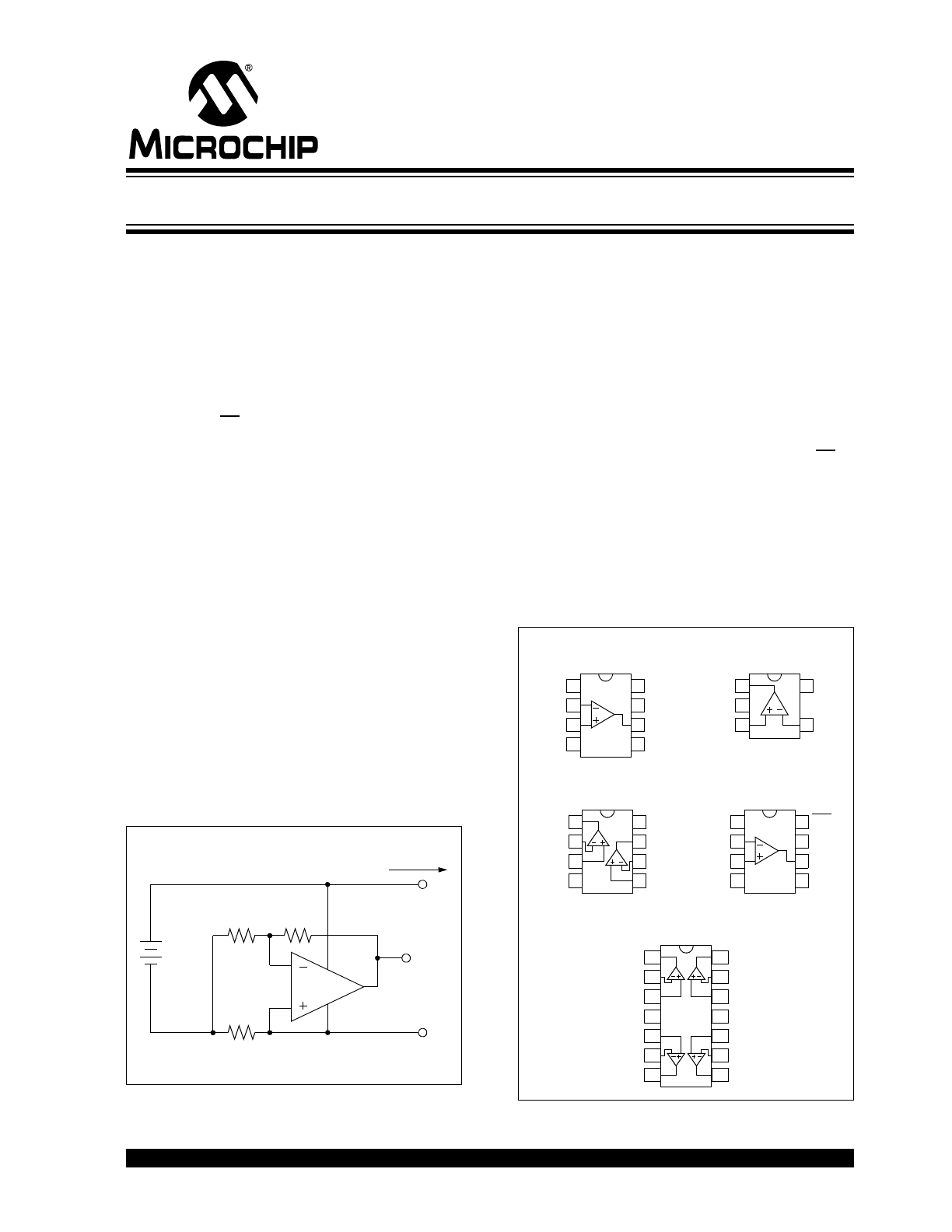
Typical Application
Description
The MCP606/7/8/9 family of operational amplifiers (op
amps) from Microchip Technology Inc. are unity-gain
stable with low offset voltage (250 µV, maximum).
Performance characteristics include rail-to-rail output
swing capability and low input bias current (80 pA at
+85°C, maximum). These features make this family of
op amps well suited for single-supply, precision,
high-impedance, battery-powered applications.
The single is available in standard 8-lead PDIP, SOIC
and TSSOP packages, as well as in a SOT-23-5
package. The single MCP608 with Chip Select (CS) is
offered in the standard 8-lead PDIP, SOIC and TSSOP
packages. The dual MCP607 is offered in the standard
8-lead PDIP, SOIC and TSSOP packages. Finally, the
quad MCP609 is offered in the standard 14-lead PDIP,
SOIC and TSSOP packages. All devices are fully
specified from -40°C to +85°C, with power supplies
from 2.5V to 6.0V.
Package Types
Low-Side Battery Current Sensor
R
F
To Load
2.5V
R
G
5 k
Ω
50 k
Ω
To Load
V
OUT
R
SEN
10
Ω
(V
LM
)
(V
LP
)
I
L
to
6.0V
V
OUT
V
LM
I
+
L
R
SEN
R
F
R
G
⁄
(
)
=
MCP606
V
IN
+
V
IN
–
V
SS
V
DD
V
OUT
1
2
3
4
8
7
6
5 NC
NC
NC
PDIP, SOIC,TSSOP
PDIP, SOIC,TSSOP
PDIP, SOIC,TSSOP
PDIP, SOIC,TSSOP
SOT-23-5
V
IN
+
V
SS
V
IN
–
1
2
3
5
4
V
DD
V
OUT
V
INA
+
V
INA
–
V
SS
V
OUTB
V
INB
–
1
2
3
4
8
7
6
5 V
INB
+
V
DD
V
OUTA
V
IN
+
V
IN
–
V
SS
V
DD
V
OUT
1
2
3
4
8
7
6
5 NC
CS
NC
V
INA
+
V
INA
–
V
DD
V
IND
–
V
IND
+
1
2
3
4
14
13
12
11 V
SS
V
OUTD
V
OUTA
V
INB
–
V
INB
+
V
OUTB
V
INC
+
V
INC
–
5
6
7
10
9
8 V
OUTC
MCP606
MCP606
MCP607
MCP608
MCP609
2.5V to 6.0V Micropower CMOS Op Amp

MCP606/7/8/9
DS11177F-page 2
© 2009 Microchip Technology Inc.
NOTES:
© 2009 Microchip Technology Inc.
DS11177F-page 3
MCP606/7/8/9
1.0
ELECTRICAL
CHARACTERISTICS
Absolute Maximum Ratings †
V
DD
– V
SS
........................................................................7.0V
Current at Input Pins ....................................................±2 mA
Analog Inputs (V
IN
+, V
IN
–) †† ........ V
SS
– 1.0V to V
DD
+ 1.0V
All Other Inputs and Outputs ......... V
SS
– 0.3V to V
DD
+ 0.3V
Difference Input Voltage ...................................... |V
DD
– V
SS
|
Output Short Circuit Current ................................ Continuous
Current at Output and Supply Pins ............................±30 mA
Storage Temperature ................................. –65° C to +150° C
Maximum Junction Temperature (T
J
) ........................ .+150° C
ESD Protection On All Pins (HBM; MM)
.............. ≥ 3 kV; 200V
† Notice: Stresses above those listed under “Absolute
Maximum Ratings” may cause permanent damage to the
device. This is a stress rating only and functional operation of
the device at those or any other conditions above those
indicated in the operational listings of this specification is not
implied. Exposure to maximum rating conditions for extended
periods may affect device reliability.
†† See Section 4.1.2 “Input Voltage and Current Limits”.
DC CHARACTERISTICS
Electrical Characteristics: Unless otherwise indicated, V
DD
= +2.5V to +5.5V, V
SS
= GND, T
A
= +25°C, V
CM
= V
DD
/2,
V
OUT
≈ V
DD
/2, V
L
= V
DD
/2, R
L
= 100 k
Ω to V
L
, and CS is tied low (refer to
Figure 1-2
and
Figure 1-3
).
Parameters
Sym
Min
Typ
Max
Units
Conditions
Input Offset
Input Offset Voltage
V
OS
-250
—
+250
µV
Input Offset Drift with Temperature
ΔV
OS
/
ΔT
A
—
±1.8
—
µV/°C T
A
= -40°C to +85°C
Power Supply Rejection Ratio
PSRR
80
93
—
dB
Input Bias Current and Impedance
Input Bias Current
I
B
—
1
—
pA
At Temperature
I
B
—
—
80
pA
T
A
= +85°C
Input Offset Bias Current
I
OS
—
1
—
pA
Common Mode Input Impedance
Z
CM
—
10
13
||6
—
Ω||pF
Differential Input Impedance
Z
DIFF
—
10
13
||6
—
Ω||pF
Common Mode
Common Mode Input Range
V
CMR
V
SS
– 0.3
V
DD
– 1.1
V
CMRR
≥ 75 dB
Common Mode Rejection Ratio
CMRR
75
91
—
dB
V
DD
= 5V, V
CM
= -0.3V to 3.9V
Open-Loop Gain
DC Open-Loop Gain
(Large-signal)
A
OL
105
121
—
dB
R
L
= 25 k
Ω to V
L
,
V
OUT
= 50 mV to
V
DD
– 50 mV
DC Open-Loop Gain
(Large-signal)
A
OL
100
118
—
dB
R
L
= 5 k
Ω to V
L
,
V
OUT
= 0.1V to V
DD
– 0.1V
Output
Maximum Output Voltage Swing
V
OL
, V
OH
V
SS
+ 15
—
V
DD
– 20
mV
R
L
= 25 k
Ω to V
L
,
0.5V input overdrive
V
OL
, V
OH
V
SS
+ 45
—
V
DD
– 60
mV
R
L
= 5 k
Ω to V
L
,
0.5V input overdrive
Linear Output Voltage Range
V
OUT
V
SS
+ 50
—
V
DD
– 50
mV
R
L
= 25 k
Ω to V
L
,
A
OL
≥ 105 dB
V
OUT
V
SS
+ 100
—
V
DD
– 100
mV
R
L
= 5 k
Ω to V
L
,
A
OL
≥ 100 dB
Output Short Circuit Current
I
SC
—
7
—
mA
V
DD
= 2.5V
I
SC
—
17
—
mA
V
DD
= 5.5V
Power Supply
Supply Voltage
V
DD
2.5
—
6.0
V
Quiescent Current per Amplifier
I
Q
—
18.7
25
µA
I
O
= 0
Note 1:
All parts with date codes November 2007 and later have been screened to ensure operation at V
DD
= 6.0V. However,
the other minimum and maximum specifications are measured at 2.5V and 5.5V.
MCP606/7/8/9
DS11177F-page 4
© 2009 Microchip Technology Inc.
AC CHARACTERISTICS
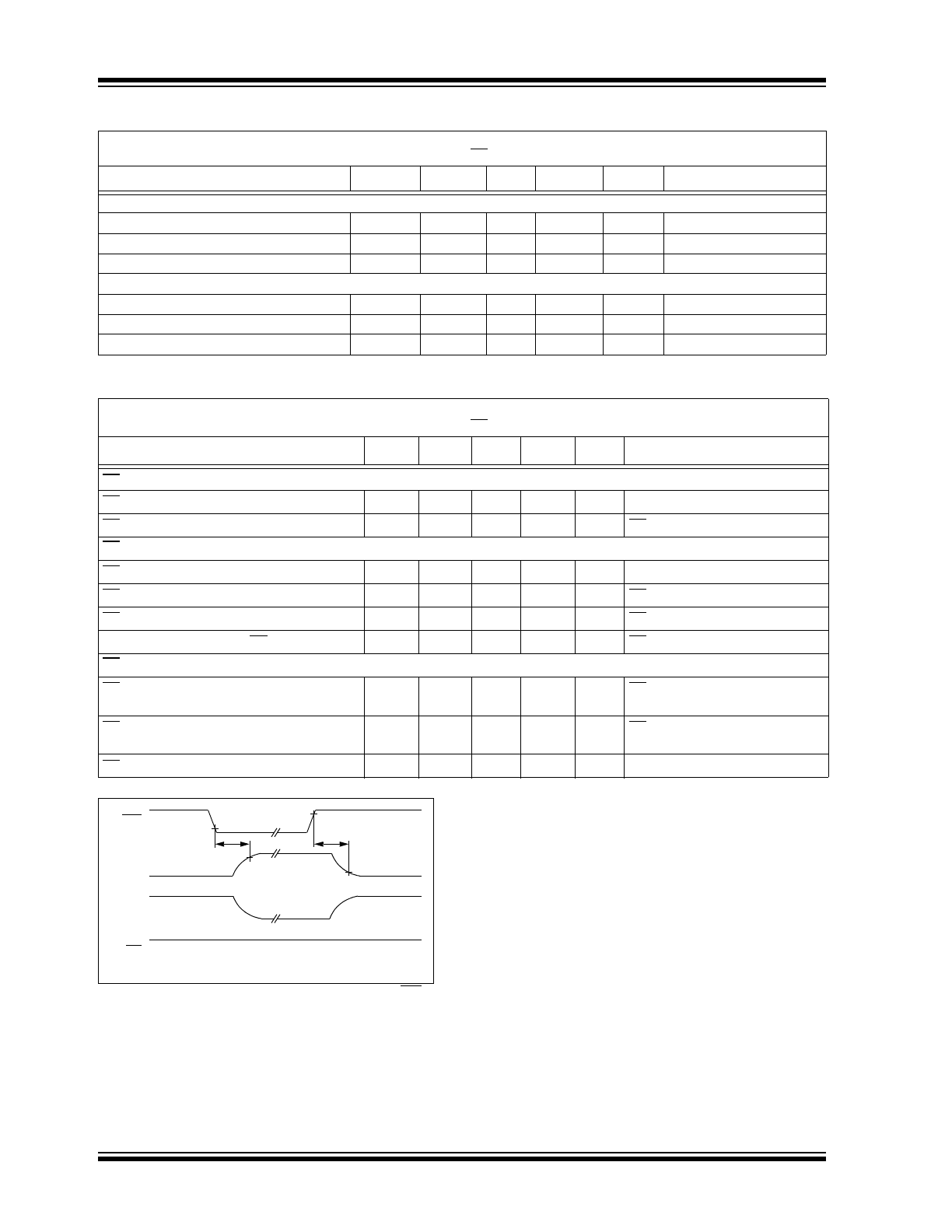
MCP608 CHIP SELECT CHARACTERISTICS
FIGURE 1-1:
Timing Diagram for the CS
Pin on the MCP608.
Electrical Characteristics: Unless otherwise indicated, V
DD
= +2.5V to +5.5V, V
SS
= GND, T
A
= +25°C, V
CM
= V
DD
/2,
V
OUT
≈ V
DD
/2, V
L
= V
DD
/2, R
L
= 100 k
Ω to V
L
and C
L
= 60 pF, and CS is tied low (refer to
Figure 1-2
and
Figure 1-3
).
Parameters
Sym
Min
Typ
Max
Units
Conditions
AC Response
Gain Bandwidth Product
GBWP
—
155
—
kHz
Phase Margin
PM
—
62
—
°
G = +1 V/V
Slew Rate
SR
—
0.08
—
V/µs
Noise
Input Noise Voltage
E
ni
—
2.8
—
µV
P-P
f = 0.1 Hz to 10 Hz
Input Noise Voltage Density
e
ni
—
38
—
nV/
√Hz f = 1 kHz
Input Noise Current Density
i
ni
—
3
—
fA/
√Hz
f = 1 kHz
Electrical Characteristics: Unless otherwise indicated, V
DD
= +2.5V to +5.5V, V
SS
= GND, T
A
= +25°C, V
CM
= V
DD
/2,
V
OUT
≈ V
DD
/2, V
L
= V
DD
/2, R
L
= 100 k
Ω to V
L
and C
L
= 60 pF, and CS is tied low (refer to
Figure 1-2
and
Figure 1-3
).
Parameters
Sym
Min
Typ
Max
Units
Conditions
CS Low Specifications
CS Logic Threshold, Low
V
IL
V
SS
—
0.2 V
DD
V
CS Input Current, Low
I
CSL
-0.1
0.01
—
µA
CS = 0.2V
DD
CS High Specifications
CS Logic Threshold, High
V
IH
0.8 V
DD
—
V
DD
V
CS Input Current, High
I
CSH
—
0.01
0.1
µA
CS = V
DD
CS Input High, GND Current
I
SS
-2
-0.05
—
µA
CS = V
DD
Amplifier Output Leakage, CS High
I
O(LEAK)
—
10
—
nA
CS = V
DD
CS Dynamic Specifications
CS Low to Amplifier Output Turn-on Time
t
ON
—
9
100
µs
CS = 0.2V
DD
to V
OUT
= 0.9 V
DD
/2,
G = +1 V/V, R
L
= 1 k
Ω to V
SS
CS High to Amplifier Output Hi-Z
t
OFF
—
0.1
—
µs
CS = 0.8V
DD
to V
OUT
= 0.1 V
DD
/2,
G = +1 V/V, R
L
= 1 k
Ω to V
SS
CS Hysteresis
V
HYST
—
0.6
—
V
V
DD
= 5.0V
CS
V
OUT
I
SS
I
CS
V
IL
V
IH
t
ON
t
OFF
-50 nA
-50 nA
-18.7 µA
-50 nA
-50 nA
Hi-Z
Hi-Z
(typical)
(typical)
(typical)
(typical)
(typical)
© 2009 Microchip Technology Inc.
DS11177F-page 5
MCP606/7/8/9
TEMPERATURE CHARACTERISTICS
1.1
Test Circuits
The test circuits used for the DC and AC tests are
shown in
Figure 1-2
and
Figure 1-3
. The bypass
capacitors are laid out according to the rules discussed
in
Section 4.5 “Supply Bypass”.
FIGURE 1-2:
AC and DC Test Circuit for
Most Non-Inverting Gain Conditions.
FIGURE 1-3:
AC and DC Test Circuit for
Most Inverting Gain Conditions.
Electrical Characteristics: Unless otherwise indicated, V
DD
= +2.5V to +5.5V and V
SS
= GND.
Parameters
Sym
Min
Typ
Max
Units
Conditions
Temperature Ranges
Specified Temperature Range
T
A
-40
—
+85
°C
Operating Temperature Range
T
A
-40
—
+125
°C
Note 1
Storage Temperature Range
T
A
-65
—
+150
°C
Thermal Package Resistances
Thermal Resistance, 5L-SOT23
θ
JA
—
220.7
—
°C/W
Thermal Resistance, 8L-PDIP
θ
JA
—
89.3
—
°C/W
Thermal Resistance, 8L-SOIC
θ
JA
—
149.5
—
°C/W
Thermal Resistance, 8L-TSSOP
θ
JA
—
139
—
°C/W
Thermal Resistance, 14L-PDIP
θ
JA
—
70
—
°C/W
Thermal Resistance, 14L-SOIC
θ
JA
—
95.3
—
°C/W
Thermal Resistance, 14L-TSSOP
θ
JA
—
100
—
°C/W
Note 1:
The MCP606/7/8/9 operate over this extended temperature range, but with reduced performance. In any case, the
Junction Temperature (T
J
) must not exceed the Absolute Maximum specification of +150°C.
V
DD
R
G
R
F
R
N
V
OUT
V
IN
V
DD
/2
1 µF
C
L
R
L
V
L
0.1 µF
MCP60X
V
DD
R
G
R
F
R
N
V
OUT
V
DD
/2
V
IN
1 µF
C
L
R
L
V
L
0.1 µF
MCP60X

MCP606/7/8/9
DS11177F-page 6
© 2009 Microchip Technology Inc.
NOTES:
© 2009 Microchip Technology Inc.
DS11177F-page 7
MCP606/7/8/9
2.0
TYPICAL PERFORMANCE CURVES
Note: Unless otherwise indicated, V
DD
= +2.5V to +5.5V, V
SS
= GND, T
A
= +25°C, V
CM
= V
DD
/2, V
OUT
≈ V
DD
/2,
V
L
= V
DD
/2, R
L
= 100 k
Ω to V
L
, C
L
= 60 pF, and CS is tied low.
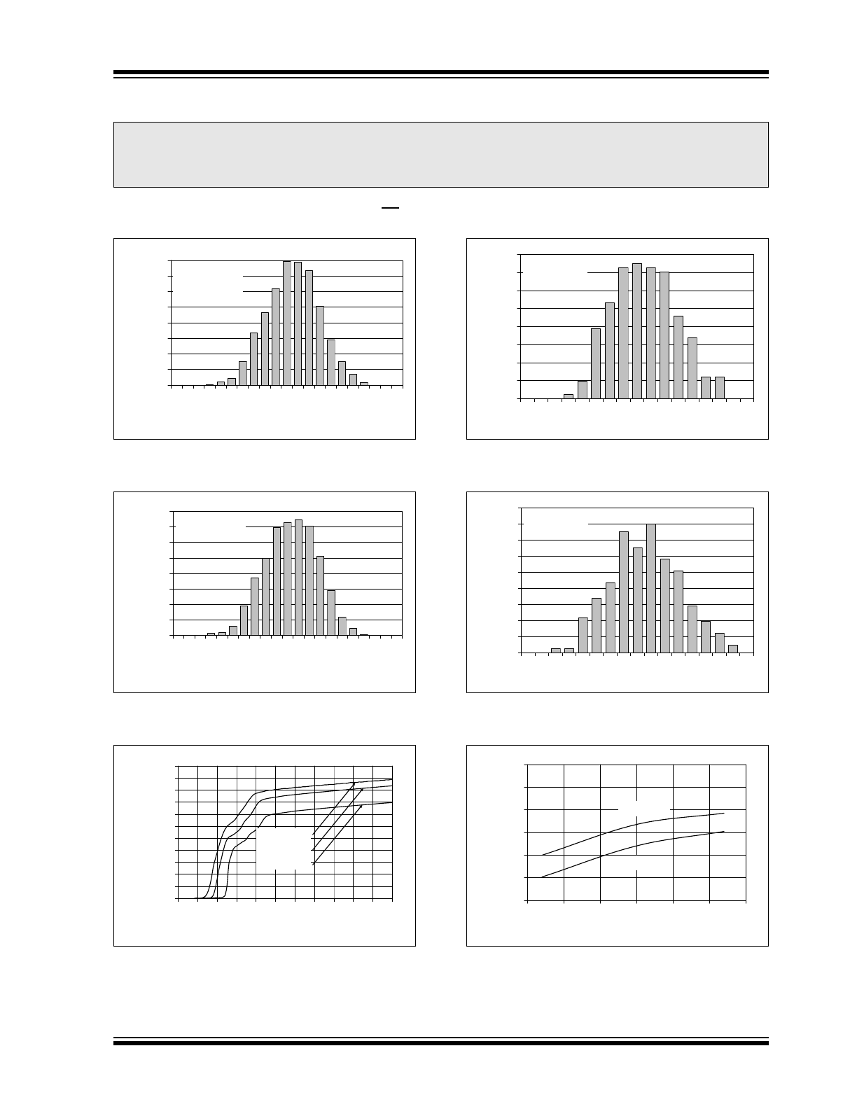
FIGURE 2-1:
Input Offset Voltage at
V
DD
= 5.5V.
FIGURE 2-2:
Input Offset Voltage at
V
DD
= 2.5V.
FIGURE 2-3:
Quiescent Current vs.
Power Supply Voltage.
FIGURE 2-4:
Input Offset Voltage Drift
Magnitude at V
DD
= 5.5V.
FIGURE 2-5:
Input Offset Voltage Drift
Magnitude at V
DD
= 2.5V.
FIGURE 2-6:
Quiescent Current vs.
Ambient Temperature.
Note:
The graphs and tables provided following this note are a statistical summary based on a limited number of
samples and are provided for informational purposes only. The performance characteristics listed herein
are not tested or guaranteed. In some graphs or tables, the data presented may be outside the specified
operating range (e.g., outside specified power supply range) and therefore outside the warranted range.
0%
2%
4%
6%
8%
10%
12%
14%
16%
-250
-200
-150
-100
-5
0
0
50
100
150
200
250
Input Offset Voltage (µV)
P
e
rcentage of
Occurances (
)
1200 Samples
V
DD
= 5.5V
0%
2%
4%
6%
8%
10%
12%
14%
16%
-2
50
-2
00
-1
50
-1
00
-5
0
0
50
10
0
15
0
20
0
25
0
Input Offset Voltage (µV)
Percent
age of Occurances (
)
1200 Samples
V
DD
= 2.5V
0
2
4
6
8
10
12
14
16
18
20
22
0.0 0.5 1.0 1.5 2.0 2.5 3.0 3.5 4.0 4.5 5.0 5.5
Power Supply Voltage (V)
Quies
c
en
t Curre
nt
pe
r Amplifier (µA)
T
A
= +85°C
T
A
= +25°C
T
A
= -40°C
0%
2%
4%
6%
8%
10%
12%
14%
16%
-8
-6
-4
-2
0
2
4
6
8
Input Offset Voltage Drift (µV/°C)
Percentage of
Occurances
206 Samples
V
DD
= 5.5V
0%
2%
4%
6%
8%
10%
12%
14%
16%
18%
-8
-6
-4
-2
0
2
4
6
8
Input Offset Voltage Drift (µV/°C)
P
e
rcentage of
Occurances
206 Samples
V
DD
= 2.5V
12
14
16
18
20
22
24
-50
-25
0
25
50
75
100
Ambient Temperature (°C)
Quie
sc
ent Current
pe
r Amplifie
r (µA)
V
DD
= 5.5V
V
DD
= 2.5V
MCP606/7/8/9
DS11177F-page 8
© 2009 Microchip Technology Inc.
Note: Unless otherwise indicated, V
DD
= +2.5V to +5.5V, V
SS
= GND, T
A
= +25°C, V
CM
= V
DD
/2, V
OUT
≈ V
DD
/2,
V
L
= V
DD
/2, R
L
= 100 k
Ω to V
L
, C
L
= 60 pF, and CS is tied low.
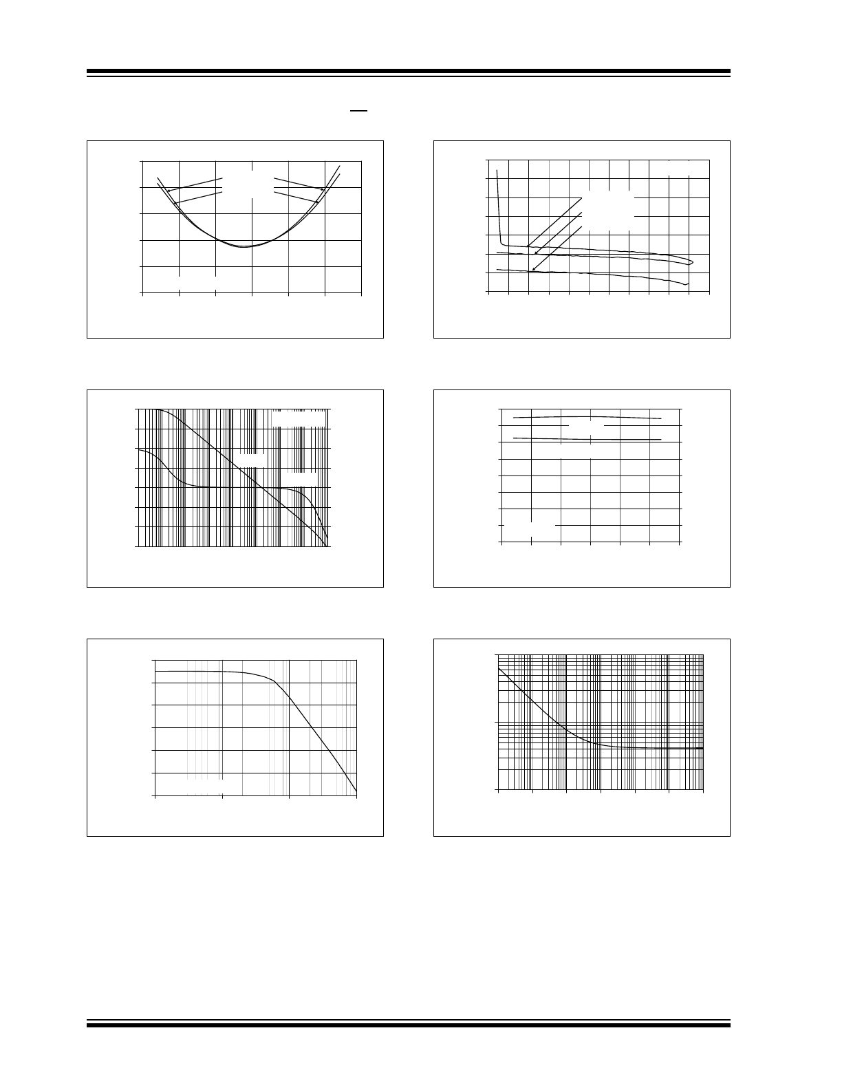
FIGURE 2-7:
Input Offset Voltage vs.
Ambient Temperature.
FIGURE 2-8:
Open-Loop Gain and Phase
vs. Frequency.
FIGURE 2-9:
Channel-to-Channel
Separation (MCP607 and MCP609 only).
FIGURE 2-10:
Input Offset Voltage vs.
Common Mode Input Voltage.
FIGURE 2-11:
Gain Bandwidth Product,
Phase Margin vs. Ambient Temperature.
FIGURE 2-12:
Input Noise Voltage Density
vs. Frequency.
0
100
200
300
400
500
-50
-25
0
25
50
75
100
Ambient Temperature (°C)
Input Of
fset
V
o
lt
age (µV)
V
DD
=2.5V
V
DD
= 5.5V
Representative Part
-20
0
20
40
60
80
100
120
Frequency (Hz)
Open-Loop Gain (dB)
-225
-180
-135
-90
-45
0
45
90
Open-Loop Phase (°
)
Gain
Phase
R
L
= 25 kΩ
0.01
1
0.1
10
1k
100
10k
1M
100k
80
90
100
110
120
130
140
1.E+02
1.E+03
1.E+04
1.E+05
Frequency (Hz)
Channel t
o
Channel
Se
p
a
ra
tio
n
(d
B
)
Referred to Input
100
100k
10k
1k
-20
0
20
40
60
80
100
120
-0
.5
0.
0
0.
5
1.
0
1.
5
2.
0
2.
5
3.
0
3.
5
4.
0
4.
5
5.
0
Common Mode Input Voltage (V)
Input
Off
s
et
V
o
lt
age (µV
)
T
A
= +85°C
T
A
= +25°C
T
A
= -40°C
V
DD
= 5.5V
0
20
40
60
80
100
120
140
160
-50
-25
0
25
50
75
100
Ambient Temperature (°C)
Gain Bandwidth Product
(k
Hz)
0
10
20
30
40
50
60
70
80
P
h
as
e M
a
rgin (
°)
Phase Margin
GBWP
V
DD
= 5.0V
10
100
1000
1.E-01 1.E+00 1.E+01 1.E+02 1.E+03 1.E+04 1.E+05
Frequency (Hz)
Input Noise V
o
lt
age Density
(nV/
√Hz)
0.1
1
10
100
1k
10k
100k
© 2009 Microchip Technology Inc.
DS11177F-page 9
MCP606/7/8/9
Note: Unless otherwise indicated, V
DD
= +2.5V to +5.5V, V
SS
= GND, T
A
= +25°C, V
CM
= V
DD
/2, V
OUT
≈ V
DD
/2,
V
L
= V
DD
/2, R
L
= 100 k
Ω to V
L
, C
L
= 60 pF, and CS is tied low.
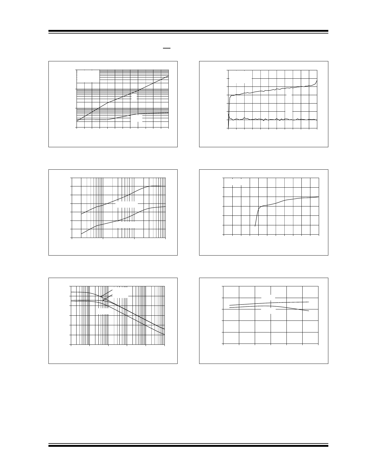
FIGURE 2-13:
Input Bias Current, Input
Offset Current vs. Ambient Temperature.
FIGURE 2-14:
DC Open-Loop Gain vs.
Load Resistance.
FIGURE 2-15:
CMRR, PSRR vs.
Frequency.
FIGURE 2-16:
Input Bias Current, Input
Offset Current vs. Common Mode Input Voltage.
FIGURE 2-17:
DC Open-Loop Gain vs.
Power Supply Voltage.
FIGURE 2-18:
CMRR, PSRR vs. Ambient
Temperature.
0.1
1
10
100
25 30 35 40 45 50 55 60 65 70 75 80 85
Ambient Temperature (°C)
Input
Bias and Of
fset
Curre
nt
s
(p
A
)
I
B
| I
OS
|
V
DD
= 5.5V
V
CM
= V
DD
100
105
110
115
120
125
130
135
1.E+02
1.E+03
1.E+04
1.E+05
Load Resistance (Ω)
DC Open
-Loop Gain (
d
B)
V
DD
= 2.5V
V
DD
= 5.5V
100
100k
10k
1k
0
20
40
60
80
100
120
1.E-01
1.E+00
1.E+01
1.E+02
1.E+03
1.E+04
Frequency (Hz)
CMRR and PSRR (
d
B
)
PSRR-
PSRR+
CMRR
0.1
1
10
100
1k
10k
-10
0
10
20
30
40
50
60
0.0 0.5 1.0 1.5 2.0 2.5 3.0 3.5 4.0 4.5 5.0 5.5
Common Mode Input Voltage (V)
In
put
Bias and Off
set
Currents
(pA)
I
B
I
OS
T
A
= 85°C
V
DD
= 5.5V
90
100
110
120
130
140
150
0.0 0.5 1.0 1.5 2.0 2.5 3.0 3.5 4.0 4.5 5.0 5.5
Power Supply Voltage (V)
DC Open-
Loop
Gain (dB)
R
L
= 25 kΩ
75
80
85
90
95
100
-50
-25
0
25
50
75
100
Ambient Temperature (°C)
CMRR and PSRR (
d
B
)
CMRR
PSRR
MCP606/7/8/9
DS11177F-page 10
© 2009 Microchip Technology Inc.
Note: Unless otherwise indicated, V
DD
= +2.5V to +5.5V, V
SS
= GND, T
A
= +25°C, V
CM
= V
DD
/2, V
OUT
≈ V
DD
/2,
V
L
= V
DD
/2, R
L
= 100 k
Ω to V
L
, C
L
= 60 pF, and CS is tied low.
FIGURE 2-19:
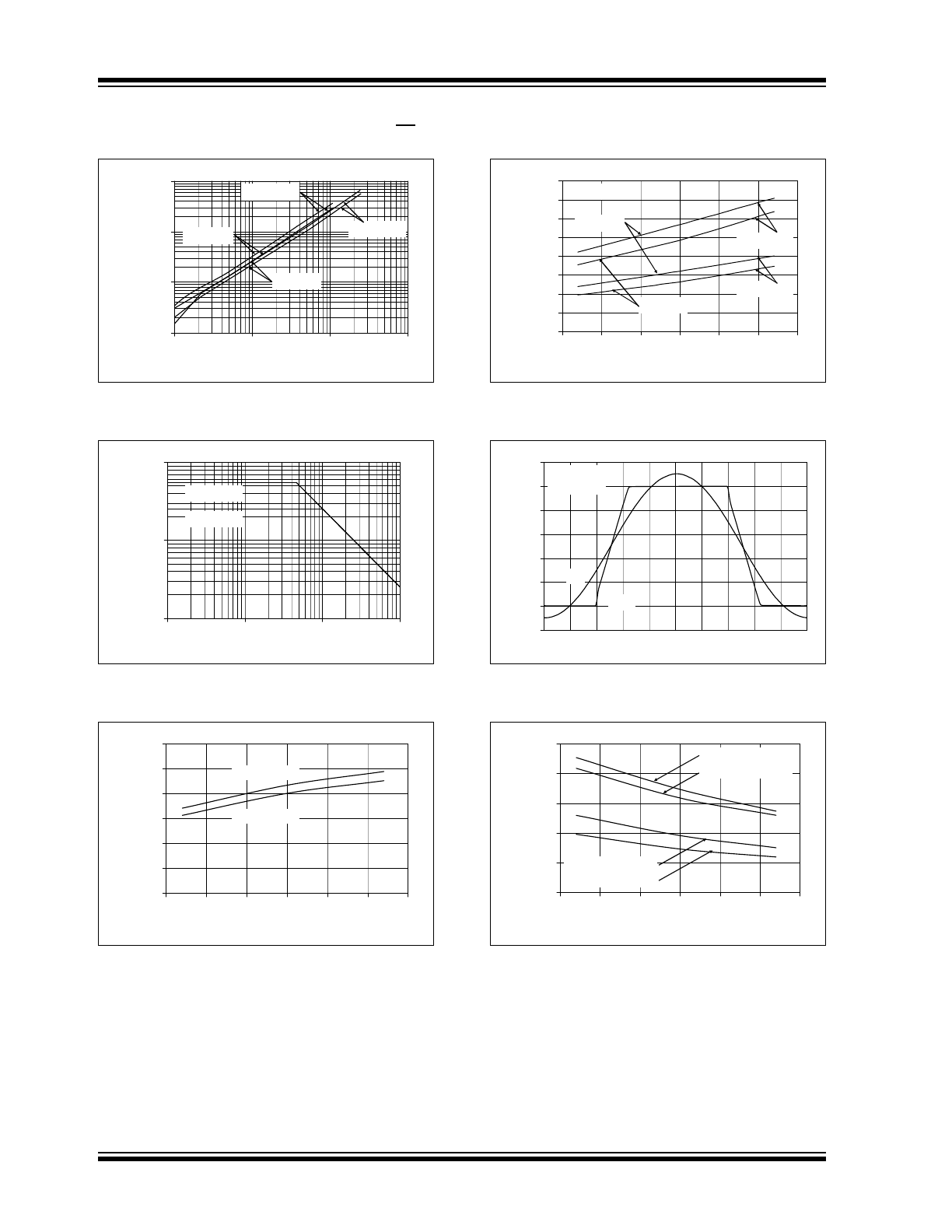
Output Voltage Headroom
vs. Output Current Magnitude.
FIGURE 2-20:
Maximum Output Voltage
Swing vs. Frequency.
FIGURE 2-21:
Slew Rate vs. Ambient
Temperature.
FIGURE 2-22:
Output Voltage Headroom
vs. Ambient Temperature at R
L
= 5 k
Ω.
FIGURE 2-23:
The MCP606/7/8/9 Show
No Phase Reversal.
FIGURE 2-24:
Output Short Circuit Current
Magnitude vs. Ambient Temperature.
1
10
100
1000
0.1
1
10
100
Output Current (mA)
Out
put Voltage Headroom
(m
V
)
V
DD
= 2.5V
V
DD
= 5.5V
V
DD
- V
OH
V
OL
- V
SS
0.1
1
10
1.E+02
1.E+03
1.E+04
1.E+05
Frequency (Hz)
M
aximum Output
V
o
lt
ag
e
S
w
ing (
V
)
V
DD
= 2.5V
100
100k
10k
1k
V
DD
= 5.5V
0.00
0.02
0.04
0.06
0.08
0.10
0.12
-50
-25
0
25
50
75
100
Ambient Temperature (°C)
S
lew R
ate
(V
/µ
s)
Low to High
High to Low
0
5
10
15
20
25
30
35
40
-50
-25
0
25
50
75
100
Ambient Temperature (°C)
O
u
tp
u
t Vo
lt
ag
e
H
e
ad
ro
o
m
(m
V)
R
L
= 5 kΩ
V
DD
= 5.5V
V
DD
= 2.5V
V
DD
- V
OH
V
OL
- V
SS
-1
0
1
2
3
4
5
6
Time (100 µs/div)
Input and Output
V
o
ltages (V)
V
OUT
V
IN
G = +2 V/V
V
DD
= 5.0V
0
5
10
15
20
25
-50
-25
0
25
50
75
100
Ambient Temperature (°C)
Ou
tput Short Circuit Current
Magnitude (mA)
+I
SC
, V
DD
= 2.5V
| -I
SC
|, V
DD
= 2.5V
+I
SC
, V
DD
= 5.5V
| -I
SC
|, V
DD
= 5.5V